
Figure: ISL Block Diagram.
Open Source Instruments Inc. (OSI) proposes to develop an Implantable Sensor with Lamp (ISL) in collaboration with the Institute of Neurology (ION) of University College London (UCL). This device will monitor electroencephalography (EEG) in a laboratory animal, identify epileptic seizures using an on-board microprocessor, and shine light upon an area of the animal's brain in response to these seizures. The device will also be able to transmit the EEG signal to an antenna outside the animal's body, and receive commands from another antenna outside the animal's body.
The problems associated with sensing, amplifying, filtering, and transmitting an EEG signal from within a water-proof, fatigue-resistant, battery-powered device implanted within a live animal are formidable. We have, however, solved these problems with our Subcutaneous Transmitter (SCT). We proposed the development of the SCT in 2004, developed it in collaboration with ION from 2005 to 2009, and prepared a paper describing the system in 2010. This paper was published in 2011.
We now propose to develop a new device for use in optogenetics animal laboratory work. We will enhance the SCT by adding a crystal radio, microprocessor, capacitor bank, and inductive boost regulators. The crystal radio will receive commands. The microprocessor will monitor the EEG signal and recognize unusual events. The capacitor bank and inductive boost regulators will provide power for a lamp. Four flexible leads will run from the new device to a head fixture. Two will carry power for the lamp and two will return the EEG signal. This new device we call the Implantable Sensor with Lamp (ISL).
The lamp will be a light-emitting diode (LED). Its light will be of a color and energy density suitable for the stimulation of opsins such as channel-rhodopsin and halo-rhodopsin. Likely colors are blue, green, and yellow, but not red. The light of the LED will be injected into an optical fiber and carried by the fiber through a hole in the skull of the subject animal. The tip of the fiber will be conical so as to shine light in all directions within the brain tissue. The combination of the LED, the fiber, and the fiber tip are what we refer to as the lamp. When we refer to lamp power, we mean the optical power emerging from the fiber tip.
| Property | Limit |
|---|---|
| Volume | 4.0 ml |
| Weight | 6 g |
| EEG Input Impedance | 10 MΩ (Note 1) |
| EEG Dynamic Range | ±10 mV (Note 1) |
| EEG Bandwidth | 160 Hz (Note 1) |
| EEG Sample Rate | 512 SPS (Note 1) |
| Lamp Instantaneous Power | 10 mW |
| Lamp Max Pulse Duration | 10 ms |
| Lamp Maximum Average Power | 1 mW |
| Lamp Wavelength | Fixed in range 400-800 nm |
| Classification Frequency | 1 Hz (Note 3) |
| Operating Range | 1 m in Faraday Enclosure |
| Shelf Life | 10 wks for 10% loss of battery capacity |
| Operating Life | 2 wks (Note 2) |
| Device Cost | $1000 US |
| Devices per Transceiver | 8 |
| Transceiver Cost | $4000 |
The lamp will be combined with EEG electrodes and a guide canula in a single head fixture. The four flexible leads will connect directly to this fixture with solder pads. Through the canula, the experimenter can inject fluids, insert a test electrode, or even feed an additional optical fiber. The EEG electrodes will be located close to the fiber so that they will monitor the same brain tissue illuminated by the fiber. The canula will be aligned so that the experimenter can treat the same tissue and check that the light is affecting its action potentials. The LED, fiber, electrodes, and canula will be combined in a single head fixture that we hope will require only one hole for insertion and alignment, and will be no more than ten millimeters high.
The microprocessor will flash the lamp when it detects particular events in the EEG signal. Or it will flash the lamp in response to commands it receives through the crystal radio. We are not yet certain how much optical power the lamp must emit to provide effective stimulation of opsins in a region sufficiently large for useful experiments. Until we determine for ourselves what power will be required, we have set for ourselves the target of 10 mW at the fiber tip. We do not have to emit this light continuously. But we would like to be able to produce 10 mW for at least 10% of the time. On average, however, we expect to be turning on the lamp for no more than 1% of the time.
If the ISL is to be practical, it must be small enough to fit inside the body of a rat, and for this we believe its volume must be no greater than 4 ml. Its battery life must be sufficient to permit the experimenter to perform a single animal study lasting two weeks.
Thus we have a maximum permissible of volume, a minimum required operating life, and a minimum lamp power. It is possible that no practical device can be built to satisfy all three of these constraints at once. If we add the requirement that the device accommodate a microprocessor and crystal radio, the difficulty of satisfying the constraints increases further. The purpose of this Conceptual Design is to demonstrate that we can indeed build a device satisfying these constraints. In the future, this design will act as a basis for the development we described in our Technical Proposal.
The figure below divides the ISL circuits into functional blocks. The entire circuit is powered from a single battery. A magnetic switch allows us to disconnect the circuit from the battery. When turned off, only the magnetic switch circuit itself receives power. When turned on, the entire circuit receives power. The lamp, however, turns on only when the microprocessor switches it on.
The ISL can receive commands through its crystal radio. By means of these commands, we can instruct the ISL to turn on its lamp, we can upload new event classification libraries, and we can request that it transmit data. We can even tell it to turn itself off. The ISL's L+ lead acts as the crystal radio antenna and as one of the lamp power leads. The other lamp power lead is L−. Like the SCT, the ISL transmits data with its radio-frequency oscillator and monitors EEG through its X leads.
Starting from the top-left, the EEG electrodes connect to the ISL X+ and X− terminals with flexible leads. We describe the development of such leads for the SCT in Flexible Wires. They are made of helical stainless steel wires insulated by silicone. Most SCT users preferred skull screws for their electrodes, but the ISL will come with bare, tinned wires at the tips of the electrodes, so that the wires may be soldered easily to the ISL's head fixture.
The incoming EEG signal is high-pass filtered, amplified, and low-pass filtered. It passes into a block of analog circuits that produce several derivatives of the original signal. These derivatives help the ISL calculate the interval metrics required by event classification. A two-pole 4-Hz high-pass filter circuit consumes only 1 μA. Implementing the same filter with digital signal processing will consume at least 10 μA. Thus we plan to perform all filtering in analog circuits.
An analog multiplexer selects one of the EEG derivatives and presents it to the Analog to Digital Converter (ADC). The ADC will be the single-input version of the sixteen-bit, micro-power ADC we used with success on A3019. The microprocessor and state machines will be implemented in a single programmable logic chip. The microprocessor will store its programs and data in a block of non-volatile memory on the same chip. These programs will remain intact even when the device is switched off.
The crystal radio receives a sequence of ones and zeros from a transmitter outside the host animal's body. Our target rate for the serial data is 8 kBit/s. Our preferred frequency for reception is 144 MHz, which is unlicensed in both the US and Europe. The design of the crystal radio is one of the ISL technical challenges.
The radio frequency oscillator will be the same as the one we used with success in the A3019. Logic levels from the logic circuits are translated into an analog frequency control by five resistors and so drive the output frequency between two values that represent ones and zeros. We describe the operation of this system, and its transmission performance, in Subcutaneous Transmitters.
The ISL power source will be a 2.7-V lithium battery. We plan to use the BR2330, which is the same battery we use in the A3019D. This battery, when combined with an efficient boost regulator, is capable of providing 10 mA to our lamp continuously. At this current, the LED will emit 12 mW. We want the lamp to produce flashes of 10 mW at the fiber tip. If we provide 20 mA in the LED, we can hope for 24 mW from the LED, of which we may be able to deliver 10 mW at the fiber tip. In this way, the ISL's capacitor bank allows us to produce 20-ms flashes of 10 mW every 50 ms.
Pulses of current flowing along the lamp's leads will induce noise on the nearby EEG leads. The lamp power supply should ramp its output voltage up slowly enough to keep this noise at an acceptable level. The lamp leads must be flexible and insulated in the same way as the EEG leads. Our starting point is the same helical leads we use for EEG pick-up in the A3019D. These have resistance 40 Ω for a length of 150 mm. We expect to bind these two leads together so as to reduce the strength of the magnetic field they generate when the lamp turns on and off. And we will do the same binding together, but separately, of the EEG leads, so as to reduce the magnetic field they pick up from the lamp leads.
We will construct the lamp out of a bare LED chip glued to a glass fiber with a tapered tip. The tapered tip will shed light in all directions sideways and forwards. Mounting the LED and bonding a wire to the LED chip is one of the ISL technical challenges. Manufacturing a tapered fiber is another technical challenge. The tapered tip must be far shorter than the tapers we have made in the past. The taper itself must be positioned with 50-μm precision with respect to the LED emitting surface and glued in place. Making a water-proof package out of the LED, the fiber tip, and the ends of the lamp leads, is another technical challenge.
We will use an LED as the source of light for our lamp. Lasers provide a smaller emitting surface, but this surface is up to 1 mm behind a glass window, which is too far for efficient direct coupling to a fiber base. Furthermore, lasers are currently available only in red and blue, with the blue ones costing $500 each. We will take LED die chips roughly 400 μm square to which we can glue the base of a 300-μm glass fiber.
We obtained samples of EZ290 bare-die LEDs made by Cree. These chips are 290-μm square. They look like dust particles to the naked eye, but with a magnifying glass and a pair of tweezers, we soldered one to a circuit board, as we show in the the following figure. The figer-tip above gives an idea of the scale of the picture.


The second photograph convinces us that we can bond to these devices with a wire-bonding machine, and subsequently glue our glass fibers in front of them. The EZ500-series LEDs have their top-side cathode contact off to one side of the light-emitting square. If we use one of these, we can bond a cathode wire to the edge of the LED and press our fiber down directly onto the light-emitting surface.

Wire-bonding and die-bonding are delicate operations requiring specialized machines. We obtained samples of the EZ500 from a distributor, and sent them to a company that provides both wire-bonding and die-bonding services. Within a week, we received twenty EZ500 LEDs, ten blue and ten green, bonded into packages with the LED surface exposed.

We will mount the LED in a small package with an open top and solder this to a flexible circuit board that we will later wrap around the frame of the head fixture. The circuit board will provide contacts for the LED power leads, contacts for the EEG leads, and a ground pad for EEG pickup. With the circuit board held by a micromanipulator, and the taper held stationary, we will raise the LED die up to the base of the fiber while looking through a microscope. When the taper is positioned correctly, we will apply UV-curing optical epoxy to the glass and LED, cure the epoxy, and be left with a taper bonded directly to a light-emitting surface.
The C460EZ500 with a forward current of 110 mA will emit 110 mW. With forward current of 20 mA, it will emit roughly 24 mW. If we glue a 300-μm diameter fiber directly to the brightest portion of the 480-μm square emitting surface, we should find that 9 mW enters the fiber. If we use the EZ290, and bring a 400-μm diameter fiber down close to the light-emitting surface, we can expect all the LED's light to enter the fiber. How much of the light will remain in the fiber is another question, which we address in the next section.
The ISL fiber captures light from the LED, carries it 7 mm through a head fixture, through a hole in the skull, and into the brain. The tip of the fiber should deliver light in all directions, including those perpendicular to the fiber axis. A fiber ending with a flat surface emits a cone of light in the forward direction. The following figure compares the light emission from a flat tip and a tapered tip. The three photographs show the light emitted from the end of 400-μm glass fibers carrying red laser light. The flat tip emits a cone of light. We can deduce the angle of the cone containing the light from the circle at the base of the beaker.


A tapered fiber tip causes light to emerge in all directions from perpendicular to the axis to along the axis. We see the lateral emission of light in the center photograph. There is no sign of a circle of light at the bottom of the beaker, and the fiber tip glows brightly in the direction of the camera lens. The photograph on the right shows a close-up of a long, slender taper. We see the light emerging uniformly along the length of the taper.
We learned how to make tapers for another project, in which we wanted to guide light into a smaller-diameter fiber. We found that the light leaked out of the taper, even when we mirror-coated its surface. But we now realize that the light emission of a taper is precisely the kind of emission that the ISL application requires. Our existing taper-making machine uses two stepper motors, a computer program, and a propane torch to stretch a fiber until a narrow waist develops. By breaking the fiber at the waist, we obtain our taper. Our light-concentrating tapers were of order ten millimeters long. The ISL requires a much shorter taper, more like a conical tip for the fiber. The following photograph shows the result of our initial efforts to make a short taper. We will study the light emission of such tapers and try to develop a heating and stretching algorithm that produces the optimal shape for tissue illumination.

If we take a 300-μm diameter glass fiber with a taper at one end and a flat surface at the other, we see that we can bring the flat surface close to our die-bonded LED chip. With the wire bond to one side, we can touch the LED surface with the fiber. With the wire bond at the center, we can bring the fiber to within 200 μm of the surface. With 20 mA supplied to the LED, and LEDs chosen for their high efficiency, we can hope for 24 mA of light at the LED surface. Our intention is to capture as much of this as possible in our fiber, and deliver it to the tapered tip. With a 400 μm diameter fiber and a 290-μm square emitting surface, we can assume that almost all the emitted power will enter the glass. The question is how much will be trapped within the fiber by total internal reflection.

At the boundary between glass (refractive index 1.5) and air (refractive index 1.0), light approaching the boundary from within the glass, making an angle θ with the perpendicular will leave the glass making angle α where sin(α) = 1.5 sin(θ). Thus if θ > 42°, α does not exist, and the light reflects back into the glass. In theory, the loss associated with this reflection is 0%. If we consider an optical fiber, however, we see that we must place some kind of jacket or cladding around the light-carrying glass. One solution is to mirror-coat the glass, but for long fibers this is ineffective. Not only is the mirror-coating is expensive and fragile, it is only 99% reflecting, so after a few hundred reflections, we will lose most of our light. In a typical multi-mode optical fiber, the 70-μm diameter core has refractive index 1.57 while the 100-μm diameter cladding has refractive index 1.52. Total internal reflection at the walls of the core takes place for angles of incidence greater than 80° to the perpendicular. Thus all rays propagating within ±10° of the fiber axis will propagate along the core without loss. It is possible, however, to make fibers with larger angles of acceptance, up to ±25°. We will experiment with such fibers.

Half the light emitted by the EZ290 is emitted in a ±22.5° cone. If we use a high numerical aperture, 300-μm core glass fiber such as the FV1204, it will capture all light within ±22.5° and transmit the light without loss. One of these fibers placed over an EZ290 would receive roughly 80% of the light it emits. Of this light entering the fiber, roughly 50% would be carried to the fiber tip. If the LED emits 24 mW, we can hope to see 20 mW entering the fiber and 10 mW emerging from the tip.
The head fixture holds the LED, the fiber, the EEG electrodes, and the canula. One of our chief concerns with the design is to reduce the noise induced in the EEG electrodes when we turn on and off the lamp. The following figures show the traces we obtained from a A3019D with its leads draped over an array of nine infra-red LEDs receiving a 10-ms pulse of 80 mA.


We see a 2-mV upward spike when the lamp turns on, and a 2-mV downward spike when it turns off. We call these the lamp switching noise. The spikes last for a few milliseconds, which is the time constant of our 160-Hz low-pass filter. In our test, the 10-ms pulse of 80 mA turns on in roughly 10 μs. In the ISL, we plan to ramp up the 20 mA drive current to the single LED over 1 ms. The voltage picked up by the EEG leads is proportional to the rate of change of current. But the duration of the pulse is inversely proportional to the rate of change of current, and it is the integral of the induced voltage that ends up being detected by our low-pass filter. Thus we cannot expect the slowing-down of our current pulse to reduce the induced noise.
The ISL peak current will be one quarter that of our test. If we can keep the EEG pickup more than 5 mm from the LED and its leads, we can hope to reduce the noise spikes by a factor of ten compared to our test. This would reduce the spikes to 200 μV. Given that baseline EEG is around 30 μV rms, we see that we must resign ourselves to serious disruption of the EEG pick-up during the turn-on and turn-off of the lamp.

The head fixture separates the LED and the EEG electrodes by 5 mm in order to reduce the lamp switching noise. The LED is mounted at the top of a plastic dome 7 mm high and 10 mm wide. The fiber penetrates down through the dome. For half its length, leading down to the base of the taper, the fiber is enclosed in a stainless steel tube. This tube serves as the X+ electrode. Its position in the plane of the skull is exact with respect to the light, and its depth is within a millimeter or two of the center of light emission. With a separate electrode lead, we run the risk of the lead and the fiber separating due to flexing or the growth of scar tissue. The steel tube is fixed rigidly with respect to the fiber and cannot be separated from the illuminated tissue by scar tissue.
During implantation, we withdraw the fiber slightly, using the flexibility of the circuit board. The taper recedes into the EEG electrode tube. Now we have two steel tubes, both soldered to the rigid portion of the circuit board, and therefore strong. We push the two tubes into the skull hole, which we can do by feel, trusting that neither tube will be bent out of place or damaged by the procedure. When the head fixture is in place, we glue it to the skull. What glue we will use, and exactly where we will place the glue will be a subject of experiment. Once the piece is glued, we press the LED down, and so push the taper out of the EEG tube and into the brain, to complete the implantation. This allows the canula, the electrode, the ground pad, and the fiber tip to be aligned perfectly with respect to one another with only one hole in the skull.
The stainless steel tube also improves transmission of light along the fiber by reflection at its inner surface. We do not allow the tube to reach up to the LED itself because we suspect that this would increase the lamp switching noise. We will, however, confirm that this suspicion is correct, because extending the tube would improve transmission down the entire length of the fiber.
The canula passes through the head fixture, terminating before it makes contact with the fiber, and staying clear of the fiber's X+ electrode. It approaches at an angle so that a syringe or electrode wire inserted down the canula an exact distance will be delivered to the illuminated tissue of the brain. The open end of the cannula outside the head fixture must be terminated with something that screws on rather than plug in, because rats are able to pull out plugs, but not to undo screws.
The head fixture has a flexible circuit to hold the LED, provide contacts for the LED power leads, and contacts for the X leads. We glue the flexible circuit to the plastic with epoxy. The bottom surface of the circuit has an exposed, gold-plated pad that serves as a ground electrode for EEG pick-up, and is connected to X−. The ground electrode touches the skull. It may also connect to the canula, so that the canula itself can be used as a ground connection for the test electrode. The canula and the fiber's stainless steel tube will both pass through vias in the circuit board, and be soldered to them so as to make reliable electrical contact.
The entire head fixture must be resistant to corrosive body fluids. We prefer the LED and electrical connections to be sealed against water except where the ground pad is exposed and where the electrode tube emerges from the fixture. But it may be that perfect water-proofing is not required in the head fixture. Provided that we seal the LED die with glue, it will remain dry. If water penetrates along the flexible circuit board, it will present the LED drive voltage with an alternative current path. But the resistance of a film of water is at least a 100 kΩ, so water will have no significant effect upon the current received by the LED when we switch it on. The rest of the time, we apply no voltage to the LED, so there will be no leakage through a water film. Our hope is that we can protect the head fixture from water by keeping the water films thin, and using solder that is resistant to corrosion in salty water.
The head fixture requires four leads: two for single-channel EEG pick-up (X+ and X−) and two to supply current to the lamp (L+ and L−). It requires one antenna, A, to transmit EEG messages and other data using 915-MHz radio waves. The L+ lead, meanwhile, will serve also as a pick-up antenna for the ISL's crystal radio. Thus we have five wires emerging from the transmitter encapsulation, which is two more than the existing A3019.
The A3019D provides 150-mm long X leads made out of helical steel wire insulated in silicone. The resistance of these wires is between 30 Ω and 40 Ω. We believe the variability in the resistance is a function of how much we stretch the initial spring to form the helix. More stretching means fewer turns in 150 mm and therefore lower resistance. A resistance of 40 Ω is negligible compared to the 10 MΩ input resistance of the EEG amplifiers, so these leads will serve well for X in the ISL.
The A3019 antenna is a 50-mm length of stranded stainless steel cable. This cable is tough and flexible, but it does not stretch. Because the antenna is attached at both ends to the ISL body, it does not have to stretch. We cannot use helical wire for the antenna because the high-frequency behavior of the helix is not favorable for omnidirectional transmission.
The L leads must carry the 20-mA drive current of the ISL's lamp. We cannot use stranded steel wire for the connection between the head fixture and the ISL body because any such connection must stretch as well as bend. Stainless steel wire bends, but it does not stretch. Thus we believe we must use helical steel wires for L, insulated with silicone. If we use the same wires as for X, their combined resistance will be up to 80 Ω. The forward voltage drop of the EZ500 is 3.4 V. If we supply 5 V to L at the lamp leads, we will see 0.8 V across the 40-Ω resistance of L+ and 0.8 V across L− also. Thus 20 mA will flow into the LED, which we believe is sufficient for the lamp power to reach 10 mW.
We can reduce the resistance of the L leads by making them out of larger gauge wire. The A3019D leads are made of 100-μm diameter steel wire. We could use 150-μm wire and reduce the resistance by a factor of two. But we must place a resistor in series with our LED anyway, to limit the flow of current. The optimal value for this resistance turns out to be close to 80 Ω, which happens to be combined resistance of our existing leads. Thus we propose to use the same leads for X and L in the ISL.
The surge of 20 mA down the L leads when the lamp turns on, and the counter-surge when the lamp turns off, will induce lamp switching noise in the X leads, as we showed above. If we can bind the L leads close together, the magnetic field they develop will be weaker. Likewise, if we can bing the X leads together, the area of the loop they present to a magnetic field will be smaller. Thus we plan to bind the L leads to one another, and the X leads to one another. We will do this with a final coat of silicone when the transmitter is otherwise complete. Binding the leads together hinders the insertion of electrode screws, but there will be no such screws in the case of the ISL. The head fixture will provide solder joints for the ends of the leads.
With the X and L leads bound as two pairs, it remains to be seen how much the proximity of these two pairs within the animal will affect the amplitude of the lamp switching noise. If the two pairs run together and parallel, the noise will be greater. It may be that we will have to develop some way to maintain a minimum distance between the two pairs, such as 5 mm, for their entire length to the head fixture. We will wait and see how severe and effect the lamp switching noise becomes, and judge whether such separation of the leads will be effective and practical.
We plan to use L+ for our command antenna. We cannot use X+ because the crystal receiver will compromise the X input's 10 MΩ impedance. When we turn on the lamp, L+ will ramp up to 5 V in roughly 2 ms. When we turn off the lamp, L+ will decay to zero with a time constant of a few milliseconds. We isolate the L+ lead from the lamp power source with an inductor whose impedance is large at the command frequency. We do the same at the other end of L+: we place an inductor on the circuit board in the head fixture, next to the lamp. At frequencies above 50 MHz, lamp switching produces no power on L+, and we can use the helical lead to pick up the command frequency.
We tried a similar arrangement to this in the A3013X transmitter, and it failed. But in that case, we were trying to use X+ lead as an EEG input and as a transmitting antenna. The inductor in series with the EEG input sometimes caused the transmit power source to oscillate and burn itself out. Other than that, the arrangement worked well. In this case, we are trying to use L+ as a receiving antenna, where there is no active amplifier that might oscillate, so we expect the dual-use of L+ to work well.
The ISL power supplies consist of a battery, a capacitor bank, 5-V inductive boost regulator, a 3.0-V inductive boost regulator, and a 1.2-V inductive buck regulator. Together we expect these components to use up a third of the board space, but the result is stable power supplies even when the battery voltage drops well below 2.0 V.
Our objective is to supply 20 mA to the LED without disturbing our analog circuits and microprocessor. With 20 mA flowing through the LED we expect the LED to produce 24 mW of light. Of this, 10 mW will emerge from the taper. With 80 Ω series resistance in the lamp leads, and a forward voltage drop of 3.4 V in the LED, we need 5.0 V at the base of the leads.
Let us begin with the battery. The capacity of a battery is typically expressed in units of mA-hrs (milliamp-hours). We BR2330 is a good choice for the ISL, this being the battery we use in the A3019D. Its rated capacity is 255 mA-hr. The total charge it can deliver is 920 C (where C is Coulomb, the unit of electrical charge).
We model real-world batteries with an ideal voltage source in series with an ideal resistor. We measure the voltage of a battery by placing a high-impedance voltmeter across its terminals. For the BR2330, the voltage source is 2.7 V. We call the resistor the battery's source resistance. We measure the source resistance by placing a low-impedance current meter across the terminals. We applied a meter to a fresh BR2330 and measured 160 mA. We tried a few other fresh ones and obtained much the same current. This suggests the source resistance of a fresh BR2330 is around 18 Ω.
According to one study, the source resistance of lithium coin batteries increases by 50% during the first half of their life, and increases rapidly after that. For the purpose of our conceptual design, we will use a simple model for our battery. Instead of its rated capacity of 920 C, we will assume its capacity is only 500 C. Instead of its measured source resistance of 18 Ω, we will assume a source resistance of 30 Ω while it delivers its 500 C of charge.
We will produce the 5 V we need for the lamp power supply with an inductive boost regulator. The LTC3525-5 together with a 10-μH inductor is 90% efficient at converting the power it draws from the battery into power it delivers at 5 V to our lamp. The regulator has an enable input. We turn on the lamp by enabling the regulator. The regulator ramps up to full power in 2 ms. The regulator and its inductor consume 10 mm2 of board area. We are now in a position to calculate the maximum current our battery can deliver to our lamp with the help of our boost regulator. We present this calculation below.

The maximum current we can deliver to the lamp is proportional to the square of the battery voltage, and inversely proportional to the source resistance. If we use 30 Ω for the battery's source resistance, 90% for the efficiency, 2.7 V for the battery voltage, and 5.0 V for the lamp supply voltage, the maximum lamp current is a little over 10 mA. The voltage at the battery terminals (x in our calculations), will be 1.35 V, and the battery current will be 45 mA.
At 10 mA, the LED emits roughly 12 mW, and of this 5 mW will emerge from the end of our fiber taper. Our specification requires 10-ms bursts of 10-mW from the fiber tip, so we need to supply around 20 mA to the LED. In order to provide this current, we will use a capacitor bank. The capacitor bank is connected across the battery terminals so that the voltage across the capacitor bank and the voltage across the battery are one and the same.
Suppose the capacitor bank is fully charged and the battery voltage is 2.7 V. We turn on the boost regulator. It supplies 20 mA at 5 V to the lamp. It draws 40 mA from the capacitor bank. Suppose the capacitor bank is 1 mF, which we can construct out of ten 100-μF capacitors that occupy 80 mm2 of board space. When delivering 40 mA, the voltage across 1 mF drops at 0.04 V/ms. When the battery voltage has dropped to 1.35 V, the boost regulator will be drawing 80 mA. Of this, 45 mA will be provided by the battery and 35 mA by the capacitor bank. During the discharge, the average current supplied by the capacitor bank is around 40 mA. The discharge takes (2.7 V − 1.35 V) ÷ 0.04 V/s = 34 ms. Thus we can turn on the lamp for 30 ms before the battery voltage drops to 1.35 V. Because the lamp's boost regulator takes 2 ms to turn on, the shortest practical flash times are around 5 ms.
A comparator in the ISL will recognize when the battery voltage drops to 1.35 V and turn off the lamp. Otherwise the battery voltage would keep dropping until the ISL shut down. Thus the ISL can provide 20 mA to the lamp for 30 ms. Once the lamp has switched off, the battery re-charges the capacitor bank. The time constant of the re-charge is 30 Ω × 1 mF = 30 ms. After 30 ms, the battery voltage has risen to 2.2 V. We can turn on the lamp again for 20 ms. The battery voltage drops to 1.35 V again. In this way, we can flash the lamp at 10 mW optical output for 20 ms out of every 50 ms, which is 40% of the time. Of course, we could instead turn on the lamp continuously with 5 mW optical output.
While providing power to the lamp, we are prepared to allow the battery voltage to drop to 1.35 V. Thus we need another inductive boost regulator to provide 3.0 V for the ISL's amplifiers, filters, ADC, 32.768 kHz oscillator, and radio-frequency oscillator. The LTC3525-3 produces 3.0-V from a battery voltage as low as 1.2 V. When delivering 100-μA at 3.0 V the device draws 130 μA from a 2.7-V input and 310 μA from a 1.2-V input.
It is very hard to make an inductive buck or boost regulator for which neither the input nor the output voltage is above 2.0 V. We want our microprocessor to be supplied with power even when the battery voltage drops to 1.35 V. To provide 1.2 V for our microprocessor, we will use the 3.0-V power supply as input to an inductive buck regulator. The LTC3620 with a 22-μH inductor takes up only 6 mm2 of board space. When our microprocessor consumes 100 μA, the buck regulator will draw 80-μA from 3.0 V. Working back through the 3.0-V boost regulator to a 2.7-V battery voltage (this being the battery voltage that will prevail whenever the lamp is turned off), we find that 100 μA to the microprocessor appears as 100 μA from the battery. Thus for a 100-μA microprocessor current, our buck regulator offers us no advantage in efficiency over a linear regulator. But it may be that we have underestimated the microprocessor current by a factor of two. If that's the case, and it draws 200-μA, this will appear as 140 μA from the battery. We plan to include this buck regulator as insurance against the microprocessor current being higher than expected.
To turn on the ISL circuit, we enable the 3.0-V boost regulator and the 1.2-V buck regulator. To turn on the lamp, we enable the 5.0-V boost regulator. Turning on the lamp will be the job of the microprocessor. Turning on the ISL circuit will be the job of the magnetic switch. The final power supply problem we must solve is that of supplying power to the magnetic switch itself. We plan to use the A1171 Hall-effect sensor, which requires a supply voltage between 1.65 V and 3.5 V. We will do this with the help of two diodes. One diode provides a path for current to flow from the battery to the sensor and the other provides a path for current to flow from the 3.0 V power supply to the sensor. When the 3.0 V power is off, the lamp will be off also, and the battery voltage will be 2.7 V. After a diode drop, the sensor will get 2.0 V, which is enough. When the 3.0 V power is on, the sensor will get 2.3 V, but no current will flow from 3.0 V to the battery because the first diode will now be reverse-biased. Thus we see that when the lamp turns on and the battery drops to 1.35 V, the sensor will be unaffected.
The magnetic switch will use the A1171 Hall-effect sensor, which is the same device we used in the A3019. As we describe above, the A1171 will receive power from the battery when the ISL is off, and from the 3.0 V power supply when the ISL is on.
To see how the magnetic switch will work, let us start by assuming the ISL is off. The A1171 draws its 5-μA quiescent current through a diode from the battery. Its output is connected through a first 1-MΩ resistor to the enable input of the 3.0-V boost regulator and through a second 1-MΩ resistor to a pin on our logic chip. Because the A1171 output is normally 0 V, no current flows through either of these resistors.
We bring a magnet near. The A1171 output jumps to 2.0 V. Through the first resistor, this voltage turns on the 3.0-V boost regulator. The 3.0 V power supply ramps up. The A1171 output rises to 2.3 V and the 1.2 V buck regulator turns on. The 1.2-V logic power ramps up. The logic chip applies to the enable input of the 3.0 V boost regulator a 3.0 V logic level through a diode.
We move the magnet away. The A1171 output drops to 0 V. But the 3.0 V regulator remains on because the logic chip continues to hold its enable input high. A current of around 2 μA flows through a diode and a the first resistor. No current flows through the second resistor.
We move the magnet close again. The A1171 output jumps to 2.3 V. The logic chip sees this transition through the second resistor and stops applying its own 3.0 V logic level to the enable input of the 3.0 V regulator. The 3.0 V regulator is kept on now by the A1171 output.
We move the magnet away and the A1171 output drops to 0 V. Through the first resistor, the enable pin of the regulator goes low. The 3.0-V boost regulator turns off, followed by the 1.2-V buck regulator. The microprocessor sees that it is losing power and turns itself off. The 3.0 V and 1.2 V power supplies drop to zero. The ISL is off.
Moving a magnet close to and then away from the ISL will turn it off when it is on or turn it on when it is off. This is the same system we used in the A3019. We see that it is not possible to turn on the ISL with a radio-frequency command. When the ISL is turned off, the microprocessor has no power. But it is possible to turn the ISL off with a radio-frequency command. Assuming there is no magnet near the ISL, the microprocessor need only drop the 3.0-V regulator's enable pin to LO, and its own power will be switched off.
The ISL transmits EEG samples and other data using its on-board radio-frequency oscillator. We have already chosen the ISL data frequency. We will use the same frequency upon which the A3019 and its predecessors transit their data: the 902-928 MHz band. The ISL will generate its data signal using the same circuit we used for the A3019. We considered switching to a more powerful transmission circuit, using a surface acoustic wave resonator and single-transistor amplifier. Such a circuit would allow us to build transmitters with a precise center frequency, thus saving us the trouble of calibrating each transmission circuit during assembly. But the challenges presented by such a development are several, and our existing transmission circuit work well, so we will continue using it.
At first, we will receive the the data signals with the same components we developed for the SCT system, but later we will modify and improve the SCT circuits. It is our intention that the data transmission and reception be fully compatible with the existing SCT system, so that SCT transmitters can share the same data acquisition system as the ISL. We will use a loop antenna to pick up ISL and SCT messages. The animals will live in a Faraday enclosures to exclude radio-frequency interference.
As we shall see, there is a risk that the ISL command signal will swamp the transmit signal at the 915-MHz loop antenna. We will improve our antenna combiner so that it rejects the command frequency more aggressively, while amplifying the data frequency just as effectively. We will design a new version of the data receiver, which integrates the antenna combiner so that we will have four antenna sockets directly on the data receiver chassis. The new data receiver will provide separate indicator lamps for all fifteen device channel numbers. We will pay particular attention to the intrusion of the command frequency through the LWDAQ power and data connections. Although we are confident that we can overcome any difficulties we face in the development of the new design, we expect to spend many hours figuring out intermittent problems with the prototypes.
The ISL's microprocessor will manage transmission of data messages by writing to an address in its memory. The microprocessor's Memory Controller (see Microprocessor and Memory) will manage the transfer of sixteen bits of data to a state machine that drives the five bit resistor DAC (digital to analog converter) that creates the input voltage to the radio-frequency oscillator. In addition to traditional data messages on channels 1-14, the ISL will be able to transmit meta-data messages on channel 15. Its microprocessor will do this by writing sixteen bits of data to a different memory address. The ISL will use meta-data messages to confirm reception of commands. The mciroprocessor will compute a checksum for a block of commands and transmit this to the data acquisition system. If the checksum is correct, the commands were received without loss or corruption, and the data acquisition system can send an execute command for the block.
The ISL receives commands by radio waves. The power consumption of the receiver must be no more than a few microamps, and the receive data rate should be at least 8 kBit/s. If possible, the radio waves that carry data to the ISL should not disrupt reception of the radio waves transmitted by this and other ISLs.
For radio reception within the ISL, we must choose a command frequency. The command frequency must itself be transmitted from an antenna outside the animal but within the Faraday enclosure, and it must be transmitted with sufficient power to stimulate the ISL's crystal radio. If we use the same frequency for data and commands, the command signal will swamp the data signal at the data antenna and the ISL will swamp its own command receiver with its own data transmissions. The only way to use the same frequency for both command and data is if the transmitters can all cooperate with one another so as to transmit one at a time. The advantage to us would be that we could use one antenna for command and data in the Faraday enclosure, and one antenna for command and data on the ISL. We would eliminate collisions between transmitters and so increase reception reliability. But coordination between transmitters is a complex process that would require many hours of testing to perfect. Furthermore, our existing subcutaneous transmitters are entirely autonomous. They would not be compatible with an ISL system that required coordination of transmitters. Thus we have decided to use two different frequencies for command and data, and two different antennas both in the ISL and in the Faraday enclosure.

We will generate the command frequency within the Faraday enclosure, using the command modulator. The command transmitter sends 15-V power pulses to the command modulator. Each pulse lasts 122 μs. During this period, the command modulator turns on and produces a 122-μs blast of command frequency power. The command transmission is a simple on-off modulation like the one we used in our SCT dummy transmission circuits. The on-off system does not work well when the transmit signal is weak and interference is strong. Under such circumstances it becomes impossible for the receiver to determine when the transmitter is not transmitting. But in the case of the ISL command transmission, the communication will take place within a Faraday enclosure, which blocks out almost all interference, and the transmit signal will be powered from the LWDAQ. It can be a thousand times stronger than the signal emitted by a battery-powered SCT. Thus we expect the simple on-off modulation to work well. Its advantage to us lies in the simplicity of the detection circuits on the ISL, where battery capacity and board space are in short supply.
If we choose a receive frequency higher than 915 MHz, multi-path interference within a Faraday enclosures will be more likely, but it will suppressed more effectively by the enclosure's microwave absorber. The absorber works better at higher frequencies. If we choose a lower frequency, we will have less multi-path interference but the absorber will be less effective. Thus multi-path interference does not give us a compelling reason to choose a frequency higher or lower than 915 MHz.
In the United States, the radio frequency spectrum is divided up like this. If possible, we would like to use one of the amateur bands (also called "unlicensed" or "industrial, scientific, and medical" bands). We would then be able to operate the system outside its Faraday enclosures and comply with Federal regulations. The table below lists all the amateur bands recognized by the FCC in the range 50 MHz to 4 GHz.
| Range (MHz) | Comment |
|---|---|
| 50-54 | Easy frequency to work with, needs large inductor for antenna matching. |
| 144-148 | Far below the frequency we know well, easy to work with. |
| 420-450 | Well-used, wide band. But second harmonic close to transmit frequency. |
| 902-928 | In use as transmit frequency. |
| 1240-1300 | Close to transmit frequency, rejection difficult. |
| 2300-2305 | Rarely-used, narrow band. |
| 2390-2450 | In use as computer WiFi. |
| 3300-3500 | Far above the frequency we know well. |
The farther our receive frequency from 915 MHz, the easier it will be to reject the command signal when we want to detect the data signal, and to reject the data signal when we want to detect the command signal. The former problem exists at the data antenna in the Faraday enclosure. The latter problem exists at the command antenna of the ISL. If we were to move to a frequency over three times higher than 915 MHz or three times lower, we will be able separate the command and data signals well enough to overcome both problems. This constrains us to 52 MHz, 146 MHz, or 3.3 GHz.
The wavelength of a 52-MHz electro-magnetic wave in open air is 6 m. In an infinitely large body of water, the wavelength drops to 0.7 m. Animal tissue is mostly water, but a rat is much smaller than 70 cm, and very much smaller than 6 m. As a result, we expect the wavelength of a 52-MHz radio wave to remain close to 6 m as it propagates through a rat's body. The same is true for a 146-MHz radio wave: in air its length is 2.1 m and in water 23 cm. A rat is no more than 0.1 m across. Once we get to 915 MHz, however, which has a 33 cm wavelength in air, we can no longer ignore the effect of animal tissue upon wavelength. In a 500-mm beaker of water, we observed the optimal length of a 915-MHz antenna dropped from 80 mm to 30 mm. At 3300 MHz, which has wavelength 9 cm in air and 1 cm in water, the wavelength inside an animal's body might be close to 1 cm, which means the optimal length of a quarter-wave dipole will be only 2.5 mm and its effective aperture only 6 mm2. An antenna that is effective in an animal body will not be effective in air, which will make testing difficult. For these reasons, we reject the 3300 MHz band. We are left with either the 52-MHz or 146-MHz bands. We expect the wavelength of these two frequencies to be close to 6 m and 2.1 m respectively even within the body of a laboratory animal. Either frequency should work well, but 146 MHz will be more convenient. The inductors and capacitors we need in the crystal receiver will be three times smaller, which will save us space. A compact antenna on the command modulator will be more efficient, because the 146 MHz wavelength is three times shorter. Thus we choose 146 MHz for our command frequency.
We now turn to the design of the command receiver circuit. This must be sensitive to command frequency power, but insensitive to data frequency power. The ISL's L+ lead will act as its command antenna. The following circuit diagram shows the lamp power source, the lead, and the lamp. The antenna picks up a radio-frequency signal of amplitude VA. The source impedance of VA is RR. At 146 MHz, RR ≈ 0.2 Ω. The series resistance of the antenna lead is RL. For our 150-mm helical leads, RL ≈ 40 Ω. Because RR << RL, we can neglect RR. The antenna includes a series capacitance, CA, which represents the capacitance between the antenna and the ground plane of the ISL circuit board.

Inductor L1 isolates the antenna from C1, so that C1 will not short VA to ground. Capacitor C3 isolates the crystal diode, D1, from the lamp switching voltage. Its impedance must be less than that of R1. Inductor L2 isolates the antenna from the lamp. Without this second inductor, the antenna would continue through the lamp and back along L−. An antenna that is folded back upon itself does not produce any radio-frequency signal.
For both 52-MHz and 146-MHz, our 150-mm antenna is a short quarter-wave antenna. An approximate analysis of such an antenna suggests that CA ≈ (2π ε l) / Ln(l / a), where l is the antenna length, a is its radius, and ε is the permittivity of the surrounding medium. Our antenna is 150 mm long and 200 μm in radius. In air, we have ε = 8.8 pF/m. If we had no insulation around our antenna or ground plane, we would have CA = 1.3 pF. In water, ε = 700 pF/m, so we would have CA = 100 pF. When implanted in a rat, the material within 100 mm will contain animal tissue, with average permittivity of around 60 pF/m. If we suppose that two thirds of the antenna surroundings are air and one third is animal tissue, we arrive at CA ≈ 20 pF when implanted in an animal.
When CA has a fixed value, we can choose L1 so that its reactance cancels that of CA at the command frequency. Such cancellation is called antenna tuning. The combination of CA and L1 would resonate at the command frequency, producing an amplified version of VA at VT. We would have VT / VA = 1 / 2π fCCARL. If we assume CA = 20 pF and fC = 146 MHz, we set L1 = 61 nH. The amplitude of VT will be 21 times higher than the amplitude of VT. In practice, however, we expect the antenna capacitance will vary from 2 pF to 40 pF depending upon its environment. At 2 pF, the gain offered by L1 = 61 nH at 146 MHz is less than the gain at 915 MHz, which means our antenna tuning will be promoting a signal we wish to reject. Thus we abandon the idea of amplifying our antenna signal with an inductor. Instead, we set L1 = 1 μH so that it will isolate the antenna from the C1, but will not promote 915 MHz.
To reject 915 MHz we must introduce some kind of filter between the antenna and our crystal diode power detector. But no filter can perform well in the presence of our variable antenna capacitance. Thus we insert a 10-kΩ resistor in series with C3 so as to isolate our filter from CA. The dynamic resistance of our crystal diode is roughly 10 kΩ, so we can now introduce a filter that operates with a source and load resistance of 10 kΩ. We make a tank circuit using inductor L3 and capacitor C4. For 146 MHz we choose L3 = 1.0 μH and C4 = 0.9 pF. When we add to C4 the parasitic capacitance of the inductor (0.1 pF) and the parallel capacitance of the crystal diode (0.2 pF), we obtain a total capacitance of 1.2 pF, and this resonates with 1.0 μH at 146 MHz. We can buy ±0.05 μH inductors and ±0.1 pF capacitors in these ranges. If we buy a reel of inductors and crystal diodes we can pick C4 to suit the components we have in hand, and so we will be confident of obtaining sharp tuning at 146 MHz. The frequency response of the resulting circuit will be as shown below. At our data frequency of 915 MHz, the tank gain is 0.015, which is thirty times smaller than at 146 MHz. Thus we have a factor of thirty rejection of the data frequency.

Now that we know R1, we pick C3 = 10 pF, so its impedance will be small compared to R1. We connect the output of our tank circuit to our crystal diode, D1. Any diode will, in theory, act as a crystal diode, but the best ones are those designed especially for the purpose. The diode presents slightly less resistance in the forward direction than in the reverse. When we apply a radio-frequency signal to one end, slightly more current flows through on the positive half-cycles than the negative. Over a large number of cycles, this discrepancy will charge up a capacitor. The capacitor will keep charging until the the average current through the diode drops to zero. In our circuit, capacitor C2 charges up when radio-frequency power is present on C3.

The above graph applies to any ideal semiconductor diode at 37°C. What distinguishes one diode from another for our purposes is the diode's effective resistance with zero bias, which is called its video resistance, which we denote RV. By zero bias we mean no average current flowing through the diode, and therefore no source of power applied to the detector circuit other than the power arriving from the antenna itself. For an ideal semiconductor diode at 37°C, we have RV = 27 mV / IS, where IS is the diode's saturation current. At this temperature, a 27-mV forward bias on the diode reduces its effective resistance to RV / e = 0.37 RV. With a 27-mV reverse bias the resistance increases to RV e = 2.7 RV. A general-purpose silicon diode has saturation current of order 30 fA, so its video resistance is of order 1 TΩ. Given the limitations of real capacitors and inductors, there is no way our tank circuit could develop an impedance of 1 MΩ at 146 MHz, let alone a million times that, so it would be impossible to perform any kind of passive tuning for a silicon diode detector with zero bias. The HSMS285C schottky diode, however, has saturation current 3 μA and RV ≈ 8 kΩ. It is especially designed for zero-bias radio-frequency power detection. We will use such a diode for D1.
We choose C2 so that the time constant of the diode resistance and the capacitor is small compared to the command bit period. We want to receive commands at 8 kBit/s, which is 125 μs/bit (in fact our bit rate will be one quarter the 32.768 kHz clock on the ISL, so that the bit period is closer to 122 μs). With 10 kΩ diode resistance, we can let C2 = 3.0 nF for a time constant of 30 μs. The bandwidth of VR will be around 5 kHz. We can feed this output to a micropower comparator. We will detect a HI bit when VR is above a threshold and a LO otherwise.
If we assume our tank circuit is tuned perfectly to the command frequency, we see that the radio-frequency amplitude we apply to our detector diode will be half the amplitude of VT. Suppose we use a comparator to compare VR to a threshold, and so translate the diode output into a logic signal. Thus our command receiver detects a logic HI when the power on its antenna exceeds a threshold, and a LO otherwise. This is a form of amplitude modulation, with one hundred percent modulation depth. A HI will correspond to a logic 1 and a LO will correspond to a logic 0. To transform the diode output to a logic level, we need a comparator. The MCP6541 from Microchip has quiescent current 0.6 μA. It can operate with a threshold of 10 mV, but not lower. If VR is to be 10 mV, the amplitude of the signal we apply to the diode must be 30 mV (referring to the graph above). The gain of our tank circuit at the command frequency is 0.5, so the amplitude of VT must be 60 mV or greater.
Suppose our command modulator radiates 1 W. Such an output is straightforward to generate using standard parts. We can place a command frequency generator within each Faraday enclosure and supply power to it with a coaxial cable. When we supply 5 V, the 146 MHz oscillator is running, but the power amplifier is off. When we raise the supply to 15 V, the power amplifiers turn on and the modulator radiates 1 W. Thus we perform the modulation with a low-frequency signal that is itself a power supply, and we keep the 146 MHz contained within each Faraday enclosure.
As a rule of thumb, the electric field strength in a favorable direction at range r from an antenna radiating power P will be 10 × √P ÷ r. At range 0.5 m in a Faraday enclosure, with 1 W radiated from the command modulator, we expect 20 V/m. Our antenna is 0.15 m long. If it is aligned parallel to the electric field, its electrical potential will oscillate with amplitude 0.15 m × 20 V/m = 3.0 V. If the antenna is unfavorably aligned or situated, our experience with reception dead spots both outside and inside Faraday enclosures suggests that we can suffer a loss of as much as 40 dB in received signal power. Instead of 3.0 V, we may obtain only 30 mV on the antenna, which is not enough to stimulate our comparator. (With 30-mV on the antenna, we have 15-mV at the input of the detector diode, and 2-mV at VR.)
Reception dead spots occur at particular frequencies. Our experience with 915 MHz in Faraday enclosures suggests that the frequency range affected by a typical dead spot is roughly 0.1% of the carrier frequency. Our 915-MHz dead spots tended to be 1 MHz wide. Our 915-MHz data transmisison has bandwidth 20 MHz on account of being modulated at 5 MHz. A 1-MHz dead spot anywhere in this 20-MHz bandwidth will compromise our signal, which is why we had so much trouble with reception dead spots in our SCT development. Our 146-MHz command transmission, on the other hand, will have bandwidth only 30 kHz, on account of being modulated at only 8 kHz. While our data transmission has bandwidth 2% of its carrier frequency, our command transmission has bandwidth only 0.02% of its carrier frequency. Our command transmission will be disrupted only by dead spots that lie within 0.1% of the carrier frequency, while our data transmission was disrupted by dead spots within 2% of the carrier frequency. Thus we expect dead spots to be twenty times less common for command reception as for data reception. Furthermore, when working with 915 MHz, which has wavelength 33 cm, we encountered reception dead spots in a 70-cm Faraday enclosure, but not in a 30-cm enclosure. Our 146-MHz command frequency has wavelength 2.1 m, so expect to see fewer reception dead spots in a 70-cm enclosure such as our FE2B.
Nevertheless, the reliability of the command transmission is a critical concern for the operation of the ISL. If we cannot rely upon commands being received by the device, we cannot rely upon flashing the lamp when the experimental procedure demands that we do so. No matter how hard we work on the radio communication, however, it is impossible to make such a connection 100% reliable without acknowledgment between the device and the command transmitter. Thus we plan to have the ISL respond to the command transmission with an acknowledgment transmission on data channel fifteen, which is a channel number we previously reserved for such functions. The program controlling the experiment will look for this acknowledgment, and if it is absent, the program will make a note of the failure to flash the lamp. By the time this failure is recognised, however, we can in general assume that it is too late to flash the light, so no action to correct the mistake can be taken. So long as such failures occur less than 5% of the time, we are confident that the experiment will still be effective.
We will determine by experiment whether a 1-W transmission at 146 MHz is sufficient to stimulate our proposed comparator. If not, we will increase the transmitter power until it is sufficient. We might think that adding an amplifier after the detector diode will solve our problem, but when we consider the square-law relationship between antenna amplitude and detector output, we find that it is hard to solve our problems with an amplifier. Suppose our antenna signal sometimes drops to 20 mV. In that case, we have 10 mV on the detector diode. The diode output will be only 1 mV. Thus we see that an amplitude that is a factor of three lower than our target will result in a diode output that is a factor of ten lower.
Meanwhile, we want to make sure that our data transmitter does not stimulate our command receiver. The transmitter radiates roughly 300 μW at 915 MHz. At range 50 mm, we can get electric field 3 V/m. If we assume 3 V/m on the first 50 mm of the antenna we will see 200 mV at the base of our antenna. Our tank circuit will attenuate this signal by another factor of thirty, resulting in 6 mV on the detector diode, resulting in a diode output of only 400 μV, which is far below our comparator threshold. Here we see that the square-law response of our detector diode serves to eliminate the data-frequency signal. A 30-mV signal, only five times greater, would produce a 10 mV output, twenty-five times greater.
Once we have a sequence of ones and zeros from the crystal receiver, we must detect within this sequence a command directed at this particular ISL. The logic that decodes the incoming commands must be sophisticated enough to eliminate interference. We are confident that we can provide sufficient error-checking with ten programmable logic gates clocked at 32.768 kHz, and this will consume no more than 1 μA from our battery. When the logic detects a valid command, it will activate the microprocessor to receive the command. This 1-μA logic consumption, and another 1 μA for our comparator, gives us a total current consumption for command reception of only 2 μA.
The amplifiers and filters are powered by the 3.0 V analog supply. We will filter and amplify the incoming EEG with the same circuits we used in the A3019D, giving a gain of 100 and a frequency band 0.7-160 Hz. We obtain what we call the raw signal. In the ISL, we pass the raw signal through further filters and circuits that make it easier for our microprocessor to calculate the interval metrics we need for event classification. For the purpose of this conceptual design, we plan to calculate transient power, event power, high-frequency power, asymmetry, spikiness, and intermittency.
For event power, we filter the raw signal to 4-160 Hz with a two-pole 4-Hz high-pass filter to produce the event signal. This we sample and record at 512 SPS. Our microprocessor calculates the average, variance, and standard deviation of the signal once per second. We use the variance as our measure of event power. We perform baseline calibration by looking at the event power every second and comparing it to the existing baseline power. If the new power is less, it becomes the new baseline power. If it is more, we increase the existing baseline power by a small amount. To obtain the event power metric, we divide the event power by the baseline power and use a sigmoidal fucntion look-up table to obtain the power metric, which must lie between zero and one.
For asymmetry, we take the average and standard deviation of the event signal and go through the event signal recording for the past second, counting how many samples are more than one standard deviation above the average and how many are more than one standard deviation below the average. For spikiness, we find the minimum and maximum sample in the past second. We convert these results into a metric with a sigmoidal-function look-up table.
For the high-frequency power metric, we filter the raw signal to 60-160 Hz using a two-pole 60-Hz filter to produce the high-frequency signal. We apply the high-frequency signal to a square-law power detector made out of a crystal diode. We describe the operation of a crystal diode power detector in Command Reception section. This crystal diode will have video resistance 1 MΩ. The HSMS285C is a suitable device. Its saturation current is 22 nA. The power detector produces a voltage whose average value is proportional to the average high-frequency signal power. We low-pass filter the power measurement with a 2-Hz with a single-pole low-pass filter and sample it at 8 SPS. By taking the average of these samples once per second we obtain our measurement of high-frequency power. With the help of a look-up table and the baseline power, we convert this measurement to our high-frequency power metric.
For intermittency, we filter the high-frequency power measurement to 4-16 Hz with a two-pole 16-Hz low-pass filter and a two-pole 4-Hz high-pass filter. Thus we obtain a signal whose amplitude is an indication of how much the high-frequency power is changing with time. We sample this power measurement at 64 SPS. Our microprocessor calculates its variance, which is our measure of the intermittency of high-frequency power. With the help of a look-up table and the baseline power, we produce the intermittency metric.
For transient power, we filter the raw signal to 0.7-4 Hz with a two-pole 4-Hz low-pass filter, sample at 16 SPS and calculate the variance. With the help of baseline power and a look-up table, we obtain the transient power metric.
Another signal we are interested in sampling is the battery voltage and the analog common-mode voltage. Neither of these require filtering before sampling. By measuring the battery voltage, in particular the manner in which it recovers from a flash of the lamp, we can measure the battery's source resistance. When the source resistance starts to rise, we know our battery is near exhaustion. The common-mode voltage is the analog ground. We use it for the
The amplifiers and filters produce seven signals that we need to sampple. They are the raw signal at 512 SPS, the event signal at 512 SPS, the high-frequency power level at 8 SPS, the intermittency power signal at 64 SPS, and the battery and analog ground voltages, which we will sample rarely. We will select one of these with an eight-way analog multiplexer, such as the DG4051A. This device consumes 1 μA, runs off our 3.0 V supply, and comes in a 2.6 mm × 1.8 mm package. We have one input to spare.
We will sample the signals with the LTC1864L. We used the LTC1865L, which is the two-channel version of the same device, in the A3019. The device consumes only 10 nC of charge in converting a signal with sixteen-bit precision in only 10 μs. We will use the single-channel version of the chip because it requires only three control lines instead of four. It turns out that logic connections to our tiny microprocessor chip will be scarce.
The ISL requires two clocks, one of 32.768 kH and another of 5 MHz. The 32.768 kH clock runs continuously when the ISL is turned on, and is the basis for sample frequency and crystal radio command reception. The 5-MHz clock provides timing for the read-out of the ADC, the transmission of data bits, and acts as a clock for the microprocessor. For the 32.768-kHz clock we will use a device similar to the ECS327KO we used on the A3019 transmitter. This device uses only 1 μA from its power supply. We will power it with 3.0 V. It is accurate to 20 ppm. Its charge consumption per clock cycle is 30 pC.
For its 5-MHz clock, the A3019 used a ring oscillator in programmable logic. This oscillator consumed 4 mA when it was turned on, but was running for only 10 μs out of every sample period, so that its contribution to the current consumption of the A3019D was only 20 μA. The ISL microprocessor will require the 5-MHz clock to be running for roughly 10% of the time, at which point this same ring oscillator would contribute 400 μA to the ISL's current consumption, when our total budget is only 410 μA.

We can build an oscillator using a single NAND gate with Schmitt Trigger inputs, as shown in the figure above. Its oscillation period is defined by the charging and discharging of a capacitor through a resistor. We have capacitor C at the gate input being charged by resistor R from its output. The 74LVC1G132 is a two-input NAND gate that comes in a five-ball BGA. The resistor charges C until voltage A reaches the upper transition threshold of the gate input, which is roughly two-thirds of the supply voltage, and the output drops low. Now C discharges until A drops to the lower transition threshold, which is roughly one-third of the supply voltage, and the output goes high. We can start and stop the oscillation at any time using the EN input.
The operating frequency of this oscillator will be roughly 1/RC. The 74LVC1G132 input capacitance is 3.5 pF. If we add another 6.5 pF to make a total of C = 10 pF, and let R = 20 kΩ, we will get something close to 5 MHz. For a 3.0-V power supply the current through the resistor iw 1.5/R = 75 μA on average. To this we add the dynamic consumption of the gate itself at 5 MHz. The 74LVC1G132's dynamic power dissipation capacitance is 18 pF, so at 5 MHz the device itself consumes 3.0 V × 18 pF × 5 MHz = 270 μA. The total consumption is 345 μA, which is ten times less than that of the A3019's ring oscillator.
We note that the current consumption of the oscillator is proportional to the supply voltage. The SN74AUP1G14 is a single inverting logic gate with Schmitt Trigger inputs that will run off a 1.2-V power supply. Its dissipation capacitance is 4 pF and its input capacitance is 1.5 pF. If we add 8.5 pF to make 10 pF, and use R = 20 kΩ, we get 5 MHz with only 54 μA.
So far, we have made up the value of C to 10 pF. We need our oscillator to be accurate to ±10% to support the transmission of data messages at a bit rate of 5 MBPS. The input capacitance of a logic gate is not something we can rely upon to ±10%. By adding an 8.5 pF capacitor that is accurate to 5% to a supposed input capacitance of 1.5 pF we see that a 50% change in the input capacitance from one device to the next will affect the combined capacitance only by 5%. Thus we can hope to build 5-MHz oscillators that consume only 54 μA and are, by construction, accurate to ±10%.
It may be, however, that the input capacitance of chips within a single batch can be relied upon to be equal to within 10%. Or it may be worthwhile to measure the oscillation frequency and choose R so as to bring the frequency within 5% of 5 MHz. The LCMXO2 device we plan to use for our microprocessor has Schmitt Trigger inputs itself, with input capacitance 5 pF and supply voltage 1.2 V. If we make an inverter with input and output on two pins of the device package, the inverter's dissipation capacitance is roughly 5 pF (according to the manufacturer's simulation software). Suppose we use the input capacitance as C and 40-kΩ for R. We expect oscillation at roughly 5 MHz and current consumption 45 μA. This oscillator consists of only one resistor outside the microprocessor package, and can be turned on and off instantly from within the device.
One or our ISL technical challenges is to figure out how to make this oscillator consistent from one circuit to the next. In the worst case, we will have to pick R for each device, as part of calibration. But we expect that sticking with parts form one reel, and choosing the value of R to suit the capacitor and gate, will allow us to build oscillators with accuracy ±5%, which is all we need to support the data transmission protocol. We are confident that we can produce 5 MHz with 5% accuracy for around 100 μA. As we will see later, we will perform our power calculations in terms of the charge drawn from the battery, this being more useful because we will be switching the oscillator on and off frequently. Our 100-μA 5-MHz oscillator draws 100 μC for each 5 Mcycles, so each cycle consumes 20 pC from 1.2 V.
The ISL requires a microprocessor and memory to perform event classification. Our choice is between using a ready-made processor or building our own in programmable logic. Once per second, this processor must calculate the metrics of the previous second of EEG. Although analog circuits perform as much information about the metrics as possible, the processor will be left with several intensive calculations. One such calculation is to determine the variance of one second's worth of sixteen-bit samples. Another is to compare the new metrics to a library of reference events, which is how we obtain the final classification of the current interval. The event library might contain a hundred events. The event library, together with recordings of the EEG signal and its derivatives, as required for metric calculation, will consume several kilobytes of memory.
The most obvious way to provide the ISL with a microprocessor is to buy a ready-made embedded processor that includes its own memory. The MSP430F1611 from Texas Instruments is a ready-made sixteen-bit microprocessor in a 10-mm square package. It contains 48 KBytes EEPROM and 10 KBytes of RAM. According to its data sheet, when running with a 1-MHz clock, it consumes only 330 μA. If we assume the average instruction takes four clock cycles, each instruction will consume 1.3 nC of battery charge. In standby mode, it consumes 1.1 μA. The chip contains a sixteen-bit hardware multiplier, three sixteen-bit timers, an ADC, a comparator, and several other potentially useful features. Surely such a device can do everything that needs to be done in the way of logic and program execution?
Unfortunately, the ready-made microprocessor does not contain programmable logic, so it cannot provide efficient state machines. Consider the decoder required by the ISL's command receiver. When implemented in programmable logic, the decoder will consume of order 2 μA while checking the command signal every 30 μs. If we were to implement such a decoder with a microprocessor, we would have to activate the microprocessor core every 30 μs so that it could look at the crystal receiver output. Once awake, MSP430F1611 would have to execute at least ten instructions to check and store the state of the receiver output. Ten instructions requires forty clock cycles. If we run at 5 MHz, this will take 8 μs. The MSP430F1611's current consumption at 5 MHz is 1.6 mA, so the average current consumption of the crystal radio decoding will be 440 μA, which is two hundred times that of our proposed programmable logic command decoder. A similar analysis applied to the data transmission state machines yields the same result.
Thus we find that the ISL must include a programmable logic chip in order to reduce the current consumption of its logic functions, and this chip must be powered up continuously so that it can monitor the crystal radio output. We could use the LC4064ZE, a newer version of the logic chip used by the A3019. The LC4064ZE comes in a 4-mm square package and has sufficient capacity to implement all ISL state machines. In this scheme, our microprocessor and state machines will consist of the 10-mm square MSP430F1611 and the 4-mm square LC4064ZE.
Given that we must provide a programmable logic chip, let us consider another solution to the microprocessor problem, in which we build our own specialized microprocessor out of programmable logic gates. The LCMXO2-1200ZE from Lattice Semiconductor is a member of their new MachXO2 family of devices. This particular version comes in a 2.5-mm square package with 19 input-output connections. Tiny though it is, the device contains 8 KBytes of SRAM, 8 KBytes of EEPROM, and 1200 programmable gates. Lattice Semiconductor provides an open-source eight-bit microprocessor that consumes only 200 gates. Let us assign 50 gates to the SCT logic, 50 gates to command reception, 200 gates to the microprocessor, and 100 gates to an eight-bit hardware multiplier. This leaves us with 800 gates that we can configure as look-up tables, program memory, or scratch memory. The following table shows how we can fit an eight-bit microprocessor with hardware multiplier into 300 logic gates.
| Component | Number | Gates Required |
|---|---|---|
| Program Counter (PC) | 1 | 16 |
| Stack Pointer (SP) | 1 | 8 |
| Index Register (IX) | 1 | 16 |
| General-Purpose Registers (R1-R8) | 8 | 64 |
| Instruction Code (IC) | 1 | 8 |
| Instruction Modifier (IM) | 1 | 8 |
| Status Register (SR) | 1 | 8 |
| Register Multiplexer (RMX) | 1 | 16 |
| Arithmetic Logic Unit (ALU) | 1 | 32 |
| Hardware Multiplier (MUL) | 1 | 100 |
| Accumulator (A) | 1 | 8 |
| Memory Controller (MC) | 1 | 8 |
| Operation Controller (OC) | 1 | 8 |
| Microprocessor | Total | 300 |
A microprocessor executes instructions one after another. The instructions themselves are stored in memory. Our programmable logic chip provides memory of several types, including fast memory immediately adjacent to the microprocessor core. In our simple design, each instruction is defined by two bytes: an eight-bit instruction code and an eight-bit instruction modifier. The instructions are stored in memory. An instruction cycle begins with the Operation Controller (OC) using the Memory Controller to read the intruction into the IC and IM registers. The Memory Controller fetches them from the address given by the Program Counter (PC). The Operation Controller now executes the instruction defined by IC and IM. The instruction might be "Load R1 with byte at location IX+n". In this case, IC specifies a single-byte load into register R1 using the Index Register (IX), and IM contains the value n.
The microprocessor has sixteen working registers. They are the eight general-purpose registers (R1-R8), the Stack Pointer (SP), either byte of the Index Register (IX0 and IX1), either byte of the Program Counter (PC0 and PC1), the IM register, and the Accumulator (A). Any one of these can be routed to the first input to the Arithmetic Logic Unit (ALU) by the Register Multiplexer (RMX). The Accumulator is always used as the second input to the ALU. The ALU's output is A itself and three status bits: Carry (CY), Zero (ZR), and Less Than Zero (LZ). The ALU performs a variety of functions. The simplest is to pass X straight through to A. Its most complex function is to multiply X and A.
We can perform an eight-bit multiplication with a sequence of twenty-four eight-bit shift operations and sixteen eight-bit additions. Each operation requires that we load the instruction code and modifier from memory, allow the result of a calculation to appear in the accumulator, and move this result into a register. Each instruction takes four clock cycles. Thus the entire multiplication takes 160 clock cycles. We plan to use a 5-MHz clock, so the multiplication will take 32 μs. The time taken by the multiplication is not as important to us as the charge it consumes. There are 200 gates in the microprocessor and roughly 10% of these will change state in each clock cycle. Each state change consumes 1 pC in the LCMXO2ZE devices. One instruction consumes 10% times; 200 × 1 pC × 4 = 80 pC. One eight-bit multiplication consumes 80 pC × 40 = 3.2 nC.
We can perform the same calculation more efficiently with an eight-bit multiplier circuit. This circuit will appear as four locations in the microprocessor memory. Two are the operands two are the product bytes. The product is a sixteen-bit number. An eight-bit multiplier circuit consumes roughly sixty gates. When we add registers for the operands and product we come to roughly a hundred. The multiplier works by allowing the product to develop through eight layers of eight gates each. The product settles to the correct value after twenty propagation delays. The LCMXO2ZE internal gate delay is around 4 ns. Thus the multiplication takes only 80 ns. We expect something like 2 state changes per gate during the multiplication. so the multiplication consumes 2 × 100 × 1 pC = 200 pC. We add to this four instructions to write the operands and read the product, and the entire process takes 3.2 μs and consumes 520 pC. The multiplier circuit is ten times faster and consumes one sixth the charge.
Let us compare our home-made and ready-made solutions by examining their performance in a typical ISL operation. The microprocessor must perform an operation we call sample accumulation a thousand times a second. It starts with a sixteen-bit sample in two registers, adds the sample to a thirty-two bit value in memory, obtains the square of the sample, adds the square to a forty-eight bit value in memory, and stores the sample itself in memory. To perform the sample accumulation we read the four-byte sum from memory (4 instructions), add the two-byte sample to the four-byte sum (4 instruction), write the four-byte sum to memory (4 instruction), square the two-byte sample (16 instructions for four eight-bit multiplications), read a six-byte sum from memory (6 instructions), add the four-byte square to the six-byte sum (6 instructions), write the six-byte sum to memory (6 instructions), write the two-byte sample to memory (2 instructions). That's 48 instructions in all. In the LCMXO2ZE this consumes 48 × 80 pC = 3.8 nC. At 5 MHz, it takes 48 × 4 ÷ 5 = 38 μs.
We must add to the consumption of the home-made processor the cost of its micro-power oscillator, which we estimated at 20 pC per clock cycle. So the sample accumulation in the home-made processor uses another 20 pC × 4 × 48 = 3.8 nC. Our total charge consumption for the sample accumulation is 7.7 nC.
To perform the sample accumulation in the ready-made microprocessor, we perform a similar sequence of steps, except that the MSP430F1611 is a sixteen-bit microprocessor that provides us with a sixteen-bit multiplier and sixteen-bit read and write instructions. The sample accumulation requires only 20 instructions or 80 clock cycles. Each instruction costs approximately 1.3 nC, so the total current consumption is 26 nC and takes 16 μs at 5 MHz.
| Feature | Ready-Made MSP430F2132 with LC4064ZE |
Home-Made LCMXO2-1200 |
|---|---|---|
| Component Area | 120 mm2 | 6 mm2 |
| Sample Accumulation Cost | 26 nC, 16 μs | 7.7 nC, 38 μs |
| Programming Connectors | 2 | 1 |
| Neuroarchiver Integration | No | Yes |
| C-Compiler Available | Yes | Yes |
| Memory | 10 KBytes SRAM 48 KBytes EEPROM |
14 KBytes SRAM 8 KBytes EEPROM |
Both microprocessor have available a C-compiler. The home-made microprocessor's compiler is a free piece of software from Lattice Semiconductor that accompanies their Mico8 IP core for the LCMXO2 devices. The ready-made microprocessor's compiler is available from Texas Instruments. Some versions are free and others are not.
The home-made microprocessor is slower, but it is more compact and more efficient. We select it for our Conceptual Design. The home-made processor will be accompanied by a home-made assembler that will run within our existing data acquisition software. Thus users on Windows, MacOS, and Linux machines will all be able to write their own code, assemble it, and upload it to the ISL directly. As an OSI-written piece of software, the assembler will of course be free for anyone to download and use.
Our home-made microprocessor will provide 14 KBytes of SRAM and 8 KBytes of EEPROM. Suppose we set aside 6 KBytes of SRAM for programs. This leaves us with 8 KBytes of EEPROM for our event library and 8 KBytes for user data. An event library of one hundred events, each with six eight-bit metrics and a type number, will occupy roughly 700 Bytes. Searching through such a library will be quick. But we would like to support libraries of several thousand events, in case such libraries prove to be more accurate than smaller ones. In that case, the library will occupy 7 kBytes, and searching through it with the simplest nearest-neighbor search routine will take a significant amount of battery power. But it turns out we can use our large memory to implement a more efficient search algorithm.
Suppose we divide the six-dimensional unit cube into 36 = 729 smaller regions, each of which is a cube itself, with side 1/3. For each region we make a list of all library events that are closest to some point in this region. Thus we know that if we pick a point in the region, the closest library event will be in this list. Given the sparse occupancy of the six-dimensional unit cube by the event libraries we have encountered so far, most regions are likely to have only one or two nearest events. Other regions might have ten or twenty. When we classify a new event, we can easily determine which region it is in, and now we have only to compare the event to the region's list of closest events. This method requires that we make two lists in addition to the event library, resulting in slightly over twice the memory consumption, but it accelerates classification by a factor of one hundred, making the search trivial.
To calculate our event metrics, we plan to store in memory a total of 1300 two-byte samples each second. This will consume 2.6 kBytes of SRAM. We can set aside 4 KBytes for a raw signal history. This history would always contain the most recent 4 s of the raw X signal at 512 SPS. We could instruct the ISL to transmit these samples when a certain event takes place, thus avoiding the cost of transmitting continuously.
According to our Technical Proposal, the ISL should be able to perform event classification and deliver an average of 100 μW to the lamp for two weeks before its battery runs out. Now that we have an idea of how each part of the ISL will function, we are in a position to estimate its current consumption and determine whether our conceptual design will meet this specification.
The capacity of the ISL's battery is 500 C, as we discussed in above. If we start with a fresh battery and run for two weeks, the average current consumption of the ISL must be less than 410 μA if we are to retain our ability to drive the lamp at full power.
Our specification assumes the lamp emit an average of 20 μW during these two weeks. When the lamp is on, it receives 20 mA from the 5-V lamp supply. It emits 10 mW at the fiber tip and the lamp power supply draws 50 mA from the battery. If the lamp is on for 0.2% of the time, the average lamp power will be 20 μW and the average current drawn from the battery will be 100 μA.
| Component | Classification and Flashing (μA) |
Transmission and Flashing (μA) |
|---|---|---|
| Lamp Power | 100 | 100 |
| Magnetic Switch | 6 | 6 |
| Clock, 32.768 kHz | 1 | 1 |
| Regulators | 15 | 15 |
| Logic Quiescent | 60 | 60 |
| Amplifiers and Filters | 30 | 30 |
| Command Reception | 2 | 2 |
| Digitization | 20 | 10 |
| Sample Accumulation | 10 | 0 |
| Sample Transmission | 0 | 40 |
| Metric Calculation | 5 | 0 |
| Classification | 0.1 | 0 |
| Approximate Total | 250 | 260 |
The microprocessor will organise the sampling of the the ISL's analog signals. During classification, we digitize the raw and event signals at 512 SPS (see above). Each sample requires the the analog multiplexer to be set up, the ADC conversion to be initiated, and the ADC to be read out. We expect each conversion to take 10 μs and to consume 20 nC, which is what we observe in the A3019. Each time we take a sample, we perform a sample accumulation so as to permit us to calculate average and variance values (see above). Each accumulation costs 10 nC and 34 μs. In all, we have something like 30 μC and 50 ms for sampling and accumulating.
At the end of each second, we calculate the average, variance, and standard deviation of the raw and event signals. Now we can go through the event signal and calculate its spikiness and asymmetry. Let us assume we can perform both these calculations for the same cost as a sample accumulation. Thus we have 5 μC and around 20 ms.
With an efficient nearest-neighbor algorithm, we will need to compare our interval metrics to no more than twenty library events. But this will occur only when the current interval is powerful enough to merit classification. We expect a powerful event no more than 10% of the time, and probably only 1% of the time. Thus the current consumption of classification will be insignificant. Searching through twenty events will require of order two thousand instructions, which will take only 200 μs.
Thus we use 50 ms of processor time every second to record and accumulate samples. This 50 ms is divided into 1024 bursts of 50 μs. At the end of each second, we spend 20 ms calculating metrics. Let us suppose we spend another 30 ms and 10 μC on operating system activities and command reception. Thus we estimate that our microprocessor will run for only 100 ms out of every second and use 45 μA. To this we must add the microprocessor's quiescent current, which is 60 μA. Thus we arrive at a total of 105 μA drawn from 1.2 V. If we have space on the ISL for a buck regulator to supply 1.2 V, this 105 μA will appear as only 60 μA at the battery. But we will not assume this is the case, so we will let the current consumed from the battery by the microprocessor be 105 μA.
We obtain our estimates of transmission and digitization current consumption from our experience with the SCT devices, whose current consumption we have studied closely. The ISL will use largely the same parts for these two functions. Because the ISL provides a 3-V power supply for our amplifiers, crystal radio, ADC, and radio-frequency oscillator, we must increase the current drawn from the battery by a factor of 3.0 ÷ 2.7 ÷ 0.9 = 1.2, where the battery voltage is usually 2.7 V and the efficiency of our 3.0-V boost regulator is 90%.
Thus we conclude that the ISL will consume roughly 250 μA while performing its own classifications, and 260 μA with external classification. If it were to perform its own classification and transmit the EEG signal, it would consume 290 μA. In any case, its current consumption is less than our maximum of 410 μA for a two-week operating life.
The shelf-life of the ISL is the length of time it takes for 10% of its battery capacity to be drained by its current consumption in the off-state. Because we turn off power to all circuits using a magnetic switch, the only current consumption of the device in its off-state is that of the magnetic switch itself. We use the same circuit as the A3019, which has consumption 5 μA. This will drain 50 C of charge from our battery in three months, which is greater than the ten weeks required by our specification.
With a high-efficiency boost regulators, a super-bright LED, a glass fiber, a convenient head fixture, a simple crystal diode receiver, a home-made microprocessor, and a promising micro-power oscillator design, our conceptual design of the ISL appears to be able to meet its specification. We expect the battery and boost regulator to be able to provide 5 mW continuous light power from the lamp's conical fiber tip. If we need to increase the light power to 10 mW, the ISL's capacitor bank will make this possible. The ISL cannot provide 10 mW of lamp power continuously, but it can do so for 40% of the time in bursts of up to 20 ms. The shortest flash time the ISL can produce is around 5 ms.
The home-made microprocessor will record the EEG signal and detect events by event classification. It will be able to turn on or flash its lamp in response to such events, or in response to commands it receives through its crystal radio. The same crystal radio will allow users to upload new classification libraries and response protocols. The device will even have enough data memory to store several seconds of EEG for transmission upon command.
We have examined the implementation of the ISL's specification in detail. We believe we have arrived at realistic solutions all of the technical challenges that the specification entails. We are confident that we will be able to overcome the unforeseen challenges that arise.
For our work on the ISL development, please see our ISL Development website.
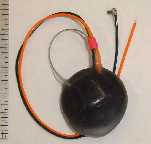
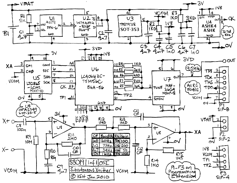
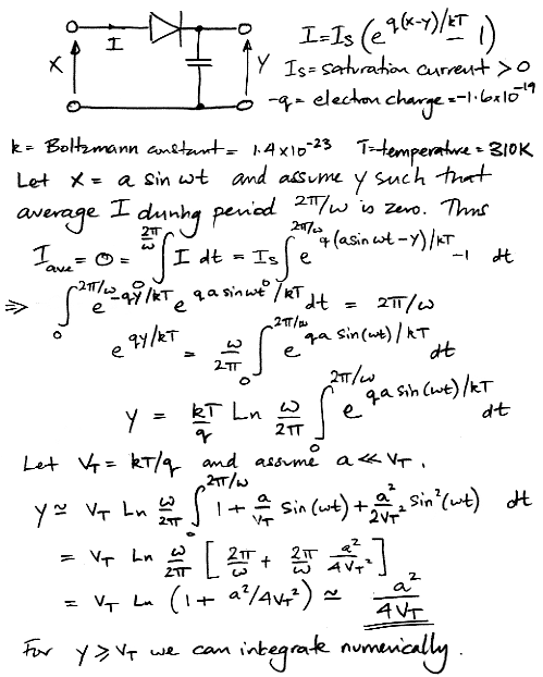