A BCAM (pronounced "beecam") is an optical surveying instrument (Boston CCD Angle Monitor). The H-BCAM Head (A3025) is a Long-Wire Data Acquisition (LWDAQ) Device that reads out two image sensors (ICX424 or equivalent) and drives six light sources. When the A3025 is connected to a pair of BCAM Side Heads (A3026), these light sources are four laser diodes in 5.6-mm metal packages (such as the L650P007) and two arrays of four LEDs in 3-mm plastic packages (such as the VLHW4100). The image sensor readout is identical to that of the Camera Head (A2075A), except that the A3025 provides two image sensors, and a switch for selecting the output from one or the other. When the A3025 is connected to two ICX424 Minimal Heads (A2076), it presents two such sensors as device elements one and two for BCAM image capture.

We designed the A3025A and A3025B for use in the Black and Blue H-BCAM respectively (H-BCAM is pronounced "h-beecam"). The H-BCAM was first conceived for the HIE-ISOLDE Alignment System, hence the use of the letter "H" in its name. The A3025B is a mirror image of the A3025A. Both circuits have amplifier gain chosen for use with the ICX424's single-pixel readout, as we discuss here. For quadruple-pixel readout, we reduce the gain of the output amplifiers by a factor of three so that the higher saturation voltage of the quadruple pixel will fall within the dynamic range of the converter on the LWDAQ Driver (we set R31 and R32 to 390 Ω).
| Version | Description |
|---|---|
| 3025A | Black H-BCAM Head (Optimized for Single-Pixel Readout) |
| 3025B | Blue H-BCAM Head (Optimized for Single-Pixel Readout) |
| 3025C | Black H-BCAM Head (Optimized for Quadruple-Pixel Readout) |
| 3025D | Blue H-BCAM Head (Optimized for Quadruple-Pixel Readout) |
The quadruple-pixel readout is four times faster than the single-pixel readout, because the A3025 bins blocks of four pixels together, so there are four times fewer of them to be read out by the LWDAQ Driver. The faster readout makes for faster data acquisition. Our experiments suggest that BCAM precision with single-pixel readout is 0.2 μm rms on the image sensor, and 0.3 μm for quadruple-pixel readout. For most BCAM applications, this degredation is insignificant. Furthermore, when the ICX424 image sensor has been irradiated by fast neutrons, its dark current increases. By binning four pixels together, we of course bin four times as much dark current into one pixel, which exactly balances the fact that the readout speed is four times faster, so that the net dark current per pixel remains the same. But it turns out that, in the ICX424, the saturation level of the quadruple pixel is three times higher than the saturation level of one pixel. As a result, we can tolerate three times as much neutron damage with quadruple-pixel readout as with single-pixel readout.
Due to an oversight on our part, the orientation of the six-way flex sockets on the A3025L/R are compatible with the A3026L/R H-BCAM Side Heads, but not the A2074C/E N-BCAM Laser Heads. If we want to use the A2074C/D with the A3025L/R, we must remove and rotate the six-way flex sockets on either the A2074C/D or A3025L/R.
[15-MAY-24] The A3025 introduced the first dual-ICX424AL camera. We discuss the behavior of the clock signals for the dual-sensor drive, in particular for quadruple-pixel readout, in this study.
S3025_1: Command Receiver.The A3025 is a LWDAQ Device, meeting all requirements of the LWDAQ Specification. Its sixteen command bits are allocated as follows.
| DC16 | DC15 | DC14 | DC13 | DC12 | DC11 | DC10 | DC9 | DC8 | DC7 | DC6 | DC5 | DC4 | DC3 | DC2 | DC1 |
|---|---|---|---|---|---|---|---|---|---|---|---|---|---|---|---|
| PXBN | ON6 | ON5 | ON4 | ON3 | ON2 | ON1 | CCD1 | WAKE | LB | SUB | V3 | V2 | V1 | H | RDP |
Bits ON1-ON6 turn on sources 1-6. Sources 1, 2, and 5 are connected to J4, and sources 3, 4, and 6 are connected to J5, as shown in the schematic. Both J4 and J5 are 6-way 1-mm pitch flex connectors. The allocation of sources to the connector pins is compatible with the Polar BCAM Head and Azimuthal BCAM Head, in which two laser sources were driven through each six-way connector. In the H-BCAM, we add one LED array to each of two six-way connectors, and call these sources 5 and 6. The CCD1 bit selects the first of two image sensors available on the A3025.
The SUB bit applies a pulse to the substrate of the image sensors so as to clear their image areas of charge. The V1-V3 bits control the levels of the vertical clock phases of the image sensors. The LWDAQ Driver controls the vertical clock phases directly during image readout by transmitting LWDAQ commands. The H bit enables the image sensor horizontal clocks, so that subsequent LWDAQ stop bits cause pulses on the clocks. The RDP, combined with V1 and V2 asserted, applies a read pulse to the image sensors, which transfers the image area charge into the transfer array. The PXBN bit is for pixel binning, which selects the quadruple-pixel readout. The LWDAQ Driver is responsible for combining rows of pixels through its manipulation of V1-V3 and H, but the A3025 is responsible for combining pixel columns, which it does with a double-pulse on the image sensor horizontal clock inputs. For more information on capturing images from the ICX424, see the Camera Head (A2075).
The A3025 is intended for use in the H-BCAM. The H-BCAM is the first BCAM to use the ICX424 image sensor, and the first to provide an LED flash for illuminating retroreflecting targets in its field of view. The figure below shows the black H-BCAM.
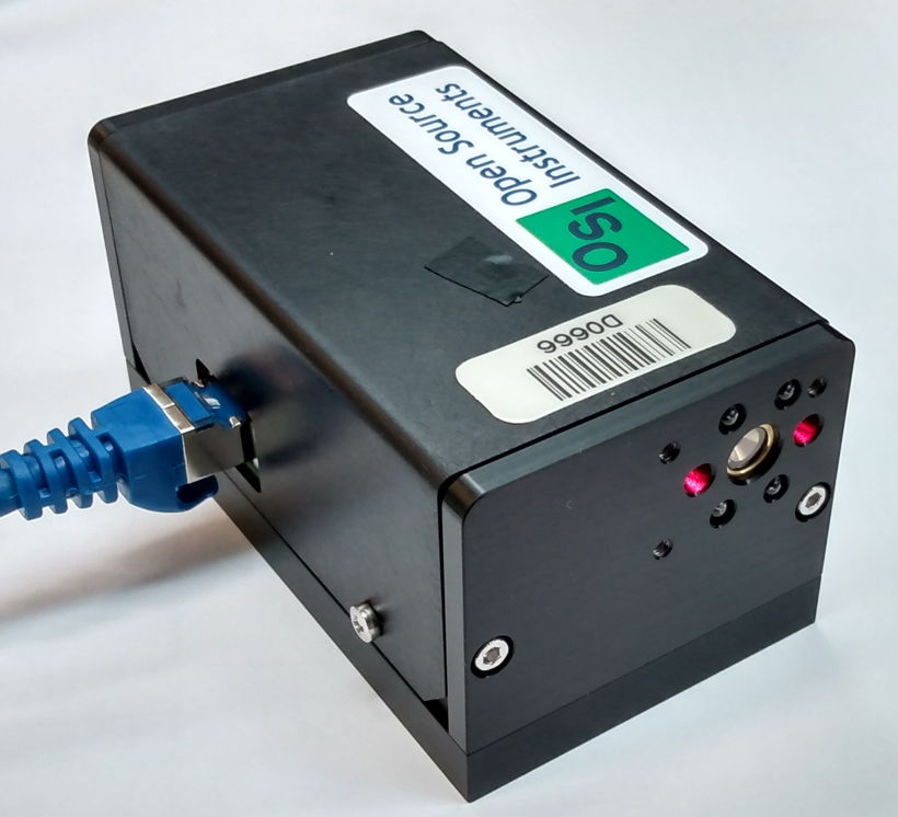
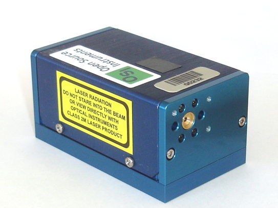
In the photograph, we see the front face with seven holes. One hole contains the brass lens-holder for the front-facing camera. The two on the left and right of the lens are for lasers. The other four holes above and below are for four white LEDs that flash to illuminate retroreflecting targets. The numbering of the four lasers is the same as for the Polar BCAMs, see here. Looking at the front face of the Black H-BCAM, Source 3 (ON3) is on the left and Source 4 (ON4) is on the right. Looking at the rear face of the Black H-BCAM, Source 1 (ON1) is on the left and Source 2 (ON2) is on the right. Source 6 is the array of four LEDs on the front face and Source 5 is the array of four LEDs on the rear face. On the Blue H-BCAM, the front-face has Source 3 (ON3) on the right and Source 4 (ON4) on the left, while the rear face has Source 1 (ON1) on the right and Source 2 (ON2) on the left.
The following figure shows what is inside the Black H-BCAM. The circuit board screwed to the base of the chassis is a Black BCAM Head (A3025A). On the front and rear walls are two Black H-BCAM Side Heads (A3026A). The image sensors are mounted on ICX424 Minimal Heads (A2076D).
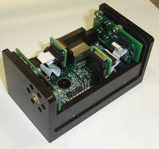
The two image sensors are glued into U-brackets, which are in turn supported by posts that are screwed to the base of the chassis. In order to replace the A3025 circuit, we must remove the two posts and the two A3026 circuits. Thus replacement of the A3025 requires re-calibration of both cameras and all four lasers. The A2076Ds connect to the A3025A with two 50-mm, 6-way flex cables. The two A2076Ds connect to the A3025A with two 50-mm, 12-way flex cables.
The A3025 can operate with only one image sensor connected, provided that image sensor is CCD2 (J3, front-facing camera). If we connect only CCD1 (J2, rear-facing camera), the image is dim and negated. The A3025 can operate with flex cables up to 300 mm provided both image sensors are plugged in. For more details see below.
[05-JAN-16] The A3025A requires no modifications. The A3025B requires a piece of kapton tape over the via that connects U1-2 through the board beneath J1. Without this tape, the via makes contact with the J1 shield.
[09-JAN-13] We have the A302501A (Black H-BCAM main board), A302601A (Black H-BCAM side board), and a prototype chassis, not anodized, with two sensor mounting pegs. We assemble them together to test the mechanical fit. See H-BCAM, Top View for photograph. The flex cables must be bent several times, but they fit in the available space. See H-BCAM, End View for photograph. The lower mounting screw of the A302601A end board requires that we go through the opposite lens hole with the screwdriver shaft. We put up with this in the Polar BCAMs, so we can tolerate it in this design too. Once the pegs are in place, however, we cannot undo the lower screw, even if we remove the lens. This we will tolerate also. See H-BCAM, Top Angle View and See H-BCAM, Side View for photographs. We recommend the following changes.
[14-JAN-13] We assemble one A302501A printed circuit board. We have difficulty with solder bridges between vias and pads, especially when the vias are obscured beneath P0805 components. But the board works with both image sensors and appears to switch its source control pins to 0V.
[01-MAR-13] We now have four working A3025As.
[04-MAR-13] We discover that the A302501A layout has J2 and J3 in the wrong place, when compared to our original schematic, which was based upon the arrangement to be found in the Polar BCAM Head (A2051L). J2 was at the front of the board, when it should have been at the back for use in the front-facing camera. This problem can be fixed in the firmware, so we produce P2074A05, in which the CCD1 signal becomes CCD2, and we modify page three of the schematic to match.
[25-MAR-13] We have two fully-functional BCAM-HLDs, loaded with 7-mW lasers set to emit 5.5±0.5 mW. Because the laser power exceeds 5 mW, we apply Class 2M laser warning labels to the sides of the BCAMs. While testing these BCAMs we notice that a light source jut above the field of view of the rear-facing camera will shine light through the lens to the top surface of the RJ-45 connector, which is shiny metal. The result is light shining onto the image sensor from a light source outside its field of view. We were able to eliminate this reflection by placing a piece of tape on one side of the connector, protruding upwards, but not by applying nail polish. We will consider how to eliminate the reflection in future versions of the H-BCAM but for now we do not modify the BCAM to remove the reflection.
[27-MAR-13] The laser holes in the Blue H-BCAM chassis are making contact with the laser cans. We insulated the cans with kapton tape. In the future, we recommend increasing the diameter of the laser holes still further.
The spacers we are using for the side baords are 0.05" thick. We are doubling them up to make 0.10" spacing between the board and the chassis.
[02-APR-13] List of issues with the H-BCAM, including hardware. Overall, the new H-BCAM works well. It is accurate and all the circuits are correct and functiona. Here are some minor problems.
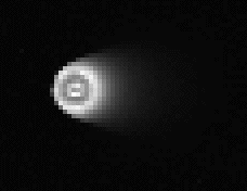
[06-AUG-13] We find that with 47-Ω resistors in place of R41, R42, R43 the H1 and H2 clocks are not formed properly in quadruple-pixel readout. This contrasts with the A2075, in which the clocks are formed properly. The A3025 loads the clock signals with two image sensors, and as a result the rise and fall time of the clock signals is longer. The 25-ns pulse required to double-clock the image sensor is attenuated. The image below shows the smearing of a BCAM image due to these poorly formed pulses in the A3025 quadruple-pixel readout.
We will solve this clocking problem in the future by replacing R41, R42, and R43 with 10-Ω resistors.
[03-SEP-13] The result of a study of double-speed clocking in the A3025 is here.
[25-SEP-13] We have an order for 56 H-BCAMs, half black and half blue. We resolve the issues listed on 02-APR-13 in the following way.
[06-JAN-15] We try various combinations of flex cables and image sensors in the two image sensor sockets, to see what kind of readout we can obtain.
| CCD1 (J2, Rear Camera) | CCD2 (J3, Front Camera) | CCD1 (Single) |
CCD1 (Quadruple) |
CCD2 (Single) |
CCD2 (Quadruple) |
|---|---|---|---|---|---|
| ICX424, 50-mm Cable | ICX424, 50-mm Cable | Perfect | Perfect | Perfect | Perfect |
| ICX424, 300-mm Cable | ICX424, 300-mm Cable | Perfect | Perfect | Perfect | Perfect |
| Omit | ICX424, 50-mm Cable | None | None | Perfect | Perfect |
| Omit | ICX424, 125-mm Cable | None | None | Perfect | Perfect |
| Omit | ICX424, 300-mm Cable | None | None | Bright pixels turn gray | Perfect |
| ICX424, 50-mm Cable | Omit | Very dim | Very dim | None | None |
| ICX424, 300-mm Cable | Omit | Very dim | Very dim | None | None |
These results show that the A3025 can operate with 300-mm flex cables, provided both image sensors are plugged in. If we want to load only one of the image sensors, it must be CCD2, but in that case the flex cable should be 125 mm or less.
As we can see, CCD2 must be loaded for CCD1 to be read out. When the A3025 wakes up to take part in a loop job, CCD2 is selected (see P2075A05.abl for firmware). The loop job measures the round-trip propagation time of the A3025's root and branch cables. If CCD2 is absent, input U11-8 to our image sensor selector switch floats to +15V, which sends a positive pulse through C12 to the output amplifier U13, resulting in a low pulse on R. The figure below shows the pulse on R− immediately after a wake command.
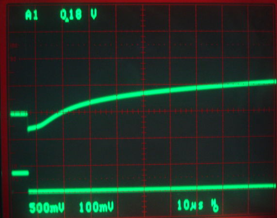
The low pulse on R corrupts the driver's measurement of loop time. The driver transmits a low pulse of its own, and is waiting for this pulse to return, but the low pulse generated by the wake-up arrives immediately, resulting in a 0-ns loop time measurement regardless of cable length. In future circuits, we will add a pull-down resistor to the image sensor outputs so that an absent image sensor does not cause pulses on R.
[30-DEC-15] We have an order for 12 Blue H-BCAMs. We have in hand 14 of the A3025B. We program them with firmware P2075A05. We capture images and flash all six light sources. The delay A to DA is 104 ns, and A to DDA is 230 ns. Ideally, these should be 125 ns and 250 ns (see specification). We adjust the firmware and get DA at 132 ns and DDA at 258 ns. We now have P3025A01.
[05-JAN-16] We have 14 A3025Bs with connectors loaded. We program and test with all sources and sensors. We add support for the A3025A/B to the Analyzer Tool. Current error for all boards is less than 5 mA.
[24-JAN-24] We update the Black H-BCAM main board layout, creating A302501C with smaller vias that we will have tented and masked. We delete the holes for CCD posts, since we have eliminated the posts. We space out the component designations so they are easy to read. We add 0V pad and power supply test points. Submit for fabrication.