 Implantable Inertial Sensor (A3035) Development and Production
© 2020-2024 Kevan Hashemi,
Open Source Instruments Inc.© 2021 Jordan Kaufmann, Open Source Instruments Inc.
| 2020 | 2021 | 2022 | 2024 |
Chronological record of the development and production of the Implantable Inertial Sensor (A3035).
[03-APR-20] We receive 25,000 custom-made rubber bands that fit around our smaller-sized implantable devices, as shown below.
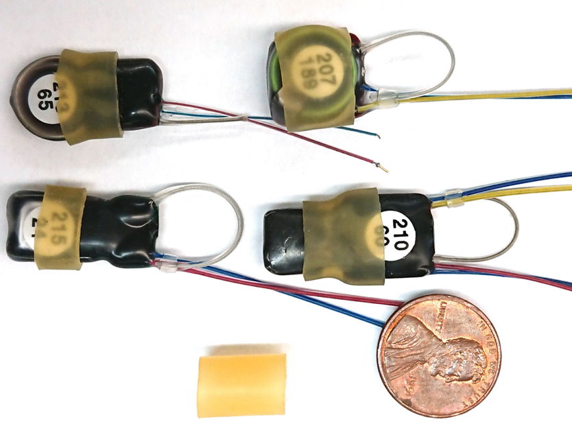
This rubber adheres well to super-glue. We can glue two bands together instantly with super-glue gel. With the rubber sleeve around the device, we can glue it to the exterior of a fish, and pull it off later. We throw away the rubber sleeve, recharge the battery, and use another sleeve for the next experiment.
[20-AUG-20] We have 100 of A303501A in 10 panels of 10.
[13-OCT-20] We have 3 of A3035AV1 first article. Inactive current consumption 1.1 μA. Turn on and we are able to scan the logic chip.
[14-OCT-20] We prepare A3035A No4 (number 0004 on circuit board label applied by assembly house) with our initital P3035A01 firmware, which does not communicate with the accelerometer or gyroscope, but instead transmits zeros at 512 SPS. We get good reception, current consumption 173 μA. We load ML920 battery, but the battery cannot supply the start-up current reequired by the LCMXO2-1200 logic chip. We try ML1220, but it can't do it either, nor a BR1225, although a BR2477 is able to get the board started, as well as a 10-mAhr LiPo battery. We can jump-start the board by attaching an external 2.6-V power supply at power up, and after that the board runs fine off its ML920.
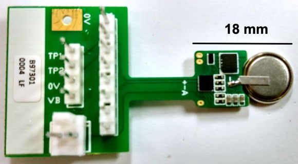
We are able to read the BMA423 accelerometer chip identifier register (0x00) and the BMG250 gyroscope sensor time register. We see the values we read from the sensors in the SCT signal plotted in the Receiver Instrument. We conclude that all connections in the circuit work, and approve second article. We leave the A3035A with 11-mAhr battery transmitting.
[16-OCT-20] After 48 hours, the A3035A is still running. Place on metal floor of our FE2F for half an hour, after which it is no longer running, and 2.5 V external power supply delivers 0.9 mA to the battery.
[21-OCT-20] We have No4 battery charged. We program No1 and No2, and re-program No4. Now each has channel number matching its board number.
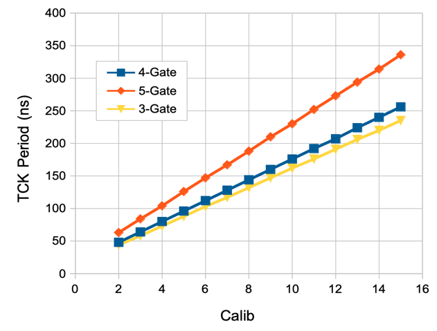
[22-OCT-20] We assign channel numbers 1, 7, and 17 to boards 1, 2, and 4 in anticipation of using six channel numbers per board for three gyroscope outputs and three accelerometer outputs. We simplify the ring oscillator, see P3035A01_OSC. We divide the ring frequency by a divisor called calib. We vary calib from 9 to 16 and measure the period of TCK and obtain the progression labelled "VHDL" in this plot. The ideal value of the period is 200 ns, with acceptable range 195-215 ns.
[23-OCT-20] We work on the serial data interface with the sensors, making sure that SCK is HI until after the falling edge of !CSA or !CSG, going HI again before the rising edge of !CSA or !CSG, and checking the setup and hold times of the outgoing address bits on SDI and the incoming data bits on SDO.
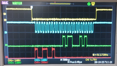
In the figure above we send address 0x0019 on SDI, which the gyroscope clocks on the rising edge of SCK. The gyroscope responds immediately after the final address bit, as shown in the detail below. On the next falling edge of SCK, we see the first data bit emerging from the gyroscope, and the A3035A accepts this bit on the rising edge of TCK, which occurs a few nanoseconds before the rising edge of SCK.
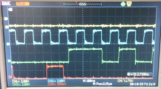
Setup time for SDI before the rising edge of SCK is 150 ns, and hold time after is 50 ns. Setup time for SDO before the rising edge of SCK is 100 ns and hold time is 100 ns. We present 24 falling and rising edges of SCK. The first eight cycles transmit the read bit and seven address bits to the gyroscope. The next 16 read out eight-bit register 0x0019 and 0x001A. The first byte is bits 8..15 of the 24-bit sensor timer. The second byte is bits 16-23. Because the gyroscope byte ordering is little-endian, we cannot read and transmit a sixteen-bit data value without storing and rearranging the bytes before-hand.
[28-OCT-20] We prepare the P3035A02 firmware, which adds a program memory, in which we store a sin wave. We transmit the gyroscope sensor timer on channel No1, and the sin wave on channel No2.
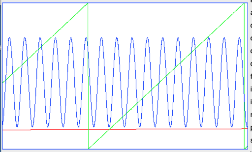
We are running at 1024 SPS, reading the gyroscope 512 times per second, and current consumption is 520 μA. When we transmit only the gyroscope timer, 512 SPS, current consumption is 150 μA.
[30-OCT-20] The excessive current consumption of P3035A02 was due to the 8-kΩ resistor on CK, which we use as a test point for !CSA and !CSG. In A3035A03 we invert the test point output to eliminate almost all this current, and now with 1024 SPS, one channel from gyroscope, one channel being read from ROM, current is 210 μA. We modify the Sample_Controller so that it uses the ROM as a program memory. We compose instructions as shown below, and fill the ROM with instructions that read two sensor timer bytes from the gyroscope and transmit them at 128 SPS.
instruction := to_integer(unsigned(prog_instr));
if (instruction = 1) then SAI <= true; else SAI <= false; end if;
if (instruction = 2) then GYSEL <= true; end if;
if (instruction = 3) then GYSEL <= false; end if;
if (instruction = 4) then SAWR <= true; end if;
if (instruction = 5) then SAWR <= false; end if;
if (instruction = 6) then sensor_addr <= "00011001"; end if;
if (instruction = 7) then sensor_addr <= "00011000"; end if;
if (instruction = 8) then xmit_bits(15 downto 8) <= sensor_byte; end if;
if (instruction = 9) then xmit_bits(7 downto 0) <= sensor_byte; end if;
if (instruction = 10) then channel_offset <= 0; end if;
if (instruction = 11) then channel_offset <= 1; end if;
if (instruction = 12) then TXI <= true; else TXI <= false; end if;
if (instruction = 0) then prog_cntr <= "00000000";
else prog_cntr <= std_logic_vector(unsigned(prog_cntr)+1); end if;
We see the sensor timer ramp pattern as before, exactly 128 SPS, and current consumption 116 μA. We adjust program to 1024 SPS and see exactly 1024 SPS at 298 μA. Cost of transmission is 0.18 μA/SPS including the two byte reads from the gyroscope.
[04-NOV-20] Our Sample_Controller now provides an instruction that loads a register A with the next byte in the program memory, and another that decrements the register A until it is zero. By this means, we can program the sample rate with the value we load into A. We set the sample rate to 512 SPS and current is 208 μA.
[07-NOV-20] We have the following Z80 instructions defined in our VHDL firmware for our embedded microprocessor. We are using little-endian byte ordering, as in the Z80, and all the same operation codes. We have 4 kBytes of ROM for instruction memory and 1 KByte of RAM for program use. The logic program now occupies 359 of 1280 look-up tables available in the logic chip (28% full).
constant nop : integer := 16#00#;
constant dec_A : integer := 16#3D#;
constant inc_A : integer := 16#3C#;
constant inc_B : integer := 16#04#;
constant dec_B : integer := 16#05#;
constant ld_A_B : integer := 16#78#;
constant ld_B_A : integer := 16#47#;
constant ld_A_n : integer := 16#3E#;
constant ld_A_mm : integer := 16#3A#;
constant ld_mm_A : integer := 16#32#;
constant jp_nn : integer := 16#C3#;
constant jp_z_nn : integer := 16#CA#;
constant jp_nz_nn : integer := 16#C2#;
We define a prototype memory map in the Z80 sixteen-bit address space.
| Reserved Range (hex) | Function | In Use (hex) |
|---|---|---|
| 0000-0FFF | Instruction Read-Only Memory | 0000-0FFF |
| 1000-1FFF | Program Random-Access Memory | 1000-13FF |
| 2000-2FFF | Gyroscope Registers | 2000-207F |
| 3000-3FFF | Accelerometer Registers | 3000-307F |
| 4000-4FFF | Transmit Registers | 4000-4002 |
Writing to addresses in the gyroscope and acceleromater ranges initiates serial access to the respective sensor. The lower six bits of the address are transmitted to the sensor. Serial access completes in 4 μs. We have three transmission control registers. Location 0x4000 is the least significant byte of a sixteen-bit data transmission, 0x4001 is the most significant, and writing n to 0x4002 initiates the transmission of sixteen bits with channel number id + n, where id is the device's ID number. Addresses 0x1000-0x13FF are 1-kByte RAM for use by the program. The program memory is read-only, and no instruction can access it other than to load instructions. We install the GNU Z80 Assembler. We use it to compile the following code, which demonstrates the use of RAM to store a value, as well as sensor reading, sample transmission, and conditional jumps.
start:
ld A,8         ; 2 load delay count into A
ld (0x1000),A  ; 3 save delay to RAM
ld A,(0x2018)  ; 4 read low byte of gyro timer
ld (0x4000),A  ; 3 write to low byte of xmit bits
ld A,(0x2019)  ; 4 read middle byte of gyro timer
ld (0x4001),A  ; 3 write to hi byte of xmit bits
ld A,0         ; 2 load A with channel offset
ld (0x4002),A  ; 3 initiate xmit
ld A,(0x1000)  ; 4 load delay from RAM
nop            ; 1
loop_1:
dec A          ; 1 decrement A
jp nz,loop_1   ; 3 loop delay (3+1)*10 = 40
jp start       ; 3 Total 64
We use a TCL script to read in the object code produced by the assembler and translate it into the line-by-line format accepted by the Lattice Diamond compiler. The above script gives us exactly 512 SPS with the gyroscope clock on channel No1, consuming 224 μA from 2.6 V.
[16-NOV-20] We now have a sufficient subset of Z80 instructions to perform arithmetic calculations, a stack, an index register, eight-bit and sixteen-bit data access cycles, and increment and decrement instructions for all seven eight-bit registers. The logic takes up around 1160 of the 1280 available LUTs (look-up tables) in the device. When we try to add CALL and RTN functions for subroutines, the design uses 1280 LUTs, and so will not fit. If we remove the increment and decrement functions for registers B, C, D, E, H, and L, the design drops to 1151 LUTs. If instead we remove INC SP, the design drops to 1276 and barely fits. We tell the compiler to keep the INC_Out bits and the design drops from 1276 to 1228. We do the same for ADD_Out and the design rises from 1228 to 1240. We undo that change. We explicitly reduce the cpu_addr, SP, and IX to 13 bits. We re-define our memory map.
| Reserved Range (hex) | Function | In Use (hex) |
|---|---|---|
| 0000-13FF | Random Access Memory (RAM), Initialized to Configuration File | 0000-13FF |
| 1400-14FF | Gyroscope Registers | 1400-147F |
| 1500-15FF | Accelerometer Registers | 1500-157F |
| 1600-16FF | Transmit Registers | 1600-1603 |
| 1700-17FF | Interrupt and Control Registers | 1700-170F |
Design drops to 1057 LUTs. We allow the compiler to merge SBYI, SBYD, SCKE and design rises to 1067 LUTs, so we restore our no-merge constraints. Timing analysis gives a maximum delay from RCK to its derivatives of 42 ns, and the compiler accepts a clock speed of 40 MHz. Current consumption of the processor at 10 MHz with 10% activity fraction is 1.1 mA. We add the LD r,n instructions and design is 1140. We remove LD r,n and add instead indirect load instructions for BC and DE as address and A as data. We are at 1085 LUTs. We do not have INC BC or INC DE, but we can increment BC, DE, or HL with the help of the carry flag, which is set when we incrment any eight-bit register, and the jump-if-carry instruction. We give instructions and clock cycles required below.
inc E      ; 1
jp c,mark1 ; 3
inc D      ; 1
mark1:
Most often, the two-register increment will take 4 clock cycles, compared to 6 for the Z80's single instruction to do the same thing. At 1085 LUTs we have space to add a few shift and rotate instructions if we find we need them for sixteen-bit arithmetic operations with signed integers. For now, we believe we have everything we need for the IIS. We can read 6144 bytes from address block 0x0000-0x13FF and write them in two-byte serial transfers to the accelerometer Features In register at 0x155E like this:
ld A,0x00      ; 3
ld B,A         ; 1
ld C,A         ; 1
ld A,0x13      ; 2
ld D,A         ; 1
ld A,0xFF      ; 2
ld E,A         ; 1
lp:
ld A,(BC)      ; 2
ld L,A         ; 1
dec C          ; 1
jp nc,m1       ; 3
dec B          ; 1
m1:
ld A,(BC)      ; 2
ld H,A         ; 1
ld (0x13FF),HL ; 4 Sixteen-bit write
dec C          ; 1
jp nc,m2       ; 3
dec D          ; 1
m2:
jp nc,lp  ; 3
Here the loop itself takes at most 20 clock cycles. If the processor runs off the IIS's 32.768 kHz clock, and the above process loads the initial value of the 6-KByte RAM into the accelerometer feature memory in 3.75 s.
[17-NOV-20] We add an Interrupt Controller to the logic, which provides four memory locations as shown in the table below. The controller generates an interrupt request signal for the processor from five possible sources: a timer, the sample transmitter, the sensor interface, and direct interrupt lines from the gyroscope and accelerometer. Our maximum timer interrupt interval is 256 ÷ 32768 = 7.8 ms. We can turn on and off individual interrupt signals with the interrupt mask and reset individual interrupts with the reset location. When the processor receives an interrupt request, it completes its current operation, then pushes the program counter onto the stack and jumps to address interrupt_pc = 0x0003. Meanwhile, the processor will start off at start_pc = 0x0000 when it powers up, so we should begin any program with a three-byte jump instruction for the start, and another three-byte jump instruction for the interrupt. We return from an interrupt with a RET instruction, and the processor will pop the program counter off the stack and continue with the previous operation. Our logic takes 1163 LUTs. We add INC SP and DEC SP back into the processor and the space required drops to 1078 LUTs.
We would like to add PUSH r and POP r for individual eight-bit registers, because these could then serve as exchange operations for all registers. But Z80 does not include a single-byte stack transfer. We would like to be able to store and set the stack pointer so that we can switch tasks, thus building a multi-threaded microprocessor that can run in a single logic chip. The LD SP,HL instruction allows us to set the stack pointer to the contents of HL. The LD (nn),SP instruction allows us to store SP in a memory location. We will implement these. We want to check that we have all the shift and rotate instructions needed for signed sixteen-bit arithmetic.
[18-NOV-20] We abandon the Z80 instruction set. Instead of providing load instructions between the registers, we provide individual eight-bit push and pop instructions PUSH r and POP r for all seven eight bit registers, plus the flags register, and two index registers IX and IY. We allow for SP, IX, and IY to be moved to and from HL. We permit arithmetic and logical operations only between A and a constant byte or register B. If we want to add H to A, without losing the current contents of B, we push B and H onto the stack, pop B then H off the stack, add B to A, then swap B and H back again. We can swap or load from one register to another through the stack. We eliminate all sixteen-bit data access, with the exception of pushing IX, IY, and PC (the program counter) onto the stack. We re-structure the sensor interface so that we write data to outgoing data bits, then initiate serial communication with another write to a control register. On reads, we initiate then read sensor bits. We select eight or sixteen-bit serial access with a control bit. The new logic is 1051 LUTs. With the 10-ns part, the maximum delay between RCK and an output is 50 ns, so we have no doubt the processor will run at 10 MHz. Our processor is untested as yet, firmware P3035A05.
We move the processor behavior definition out of our main VHDL file and into our entities file. We define the above address map with constants, and implement it with the Memory Management Unit process. We add general-purpose interrupts to the Interrupt Handler, and allow the processor to set them with the Interrupt Set Register.
[19-NOV-20] We convert our processor to big-endian byte ordering rather than little-endian. We begin work on the Open-Source Reconfigurable Eight-Bit (OSR8) Assembler-Disassembler. We add "LD HL,PC" and "LD PC,HL" to permit us to implenent relative jumps, although at the cost of copying the program counter, adding to it in the accumulator, and over-writing the program counter. We correct bugs in our implementation of PUSH and POP, and move incrementing and decrementing IX, IY, and SP into combinatorial logic to accelerate indexed read and write operations. The new code takes 1129 LUTs.
[24-NOV-20] We eliminate the separate address incrementer in our processor and perform incrementing and decrementing for SP, IX, and IY directly, which does not increase the code size. We compose our own eight-bid adder. The registers in P3035A_CPU.vhd are now global signals to permit us to refer to them outside the main CPU process. As written now, the processor uses a variable called opcode to present the current value of the program data during an opcode read state, and to store this current value for use in other states. We are using this variable to control the eight-bit adder in combinatorial logic, assuming it will be valid immediately after the rising edge of CK. But this is not the case: outside the rising-edge if-clause, the opcode variable will be updated only upon rising edges, and no such update can respond to program data that updates on the same rising edge. The result is that we need two "inc" instructions, one after the other to perform an increment, but each "dec" instruction works fine. That's because "dec" is the default.
[25-NOV-20] Quiescent current consumption of the processor stuck in a loop with no sensor or transmitter activity is 136 μA. We add to the firmware all logic needed for self-calibration of the ring oscillator. The processor writes a value to the fast clock divider. We increase the divider from 9 to 16 and reprogram the A3035A for each. The VHDL logic remains identical, only the processor program changes. Thus the ring oscillator is not re-compiled and its frequency remains the same. We plot TCK period versus divider below, and compare to the performance we obtained by adjusting a VHDL constant and re-compiling logic.

The processor can set a self-calibrate bit, which turns on the ring oscillator. The clock controller counts TCK cycles for one half RCK period. If TCK is exactly 5 MHz, we will see 76 periods. The processor reads out the count and can adjust the clock calibration constant to bring TCK to 5 MHz. With this code included in our P3035A logic, we are now at 1140 LUTs total. We are able to read out and transmit our TCK counter, and set the FCK divisor with software. Our increment, decrement, and addition instructions are working, as well as conditional jumps, pop and push, indirect loads with index registers IX and IY. If we remove registers C, D, and E from the processor the logic drops to 1080 LUTs. We restore registsers. When we examine the floorplan of the logic, we conclude that it is the processor state machine that is occupying most of the space. Add support for accelerometer SCK protocol to the Sensor Interface: SCK must be low at start of access, and rise at the same point as SCK for the gyrsoscope. With this added function, logic size drops to 1116 LUTs.
[26-NOV-20] We add to the XOR, AND, and OR instructions a set of the Z flag if A is zero and size increases to 1186 LUTs. We enhance the adder-subtractor to make an Arithmetic Logic Unit and perform our XOR, AND, and OR operations in there, so as to make the Z flag logic simpler. We add a WAIT instruction that clears the interrupt flag and stops the program counter. The processor will wait until an interrupt occurs. We add a DELAY instruction that decrements the accumulator until it is zero, then moves on. We reduce our opcodes from eight to seven bits but this causes an increase in logic size instead of a decrease.
We set the compiler option that optimizes for area rather than speed. We have seven-bit opcodes. Logic size drops from 1171 to 1086 LUTs. Now we find that the size of the code always increases with complexity of the processor. If we return to eight-bit opcodes, logic increases to 1134 LUTs. We move all the shift and rotate operations into the arithmetic logic unit, where we correct some errors in their implementation. The ALU mainpulates its inputs in response to a four-bit control signal. We have used 12 of the 16 available control values. Logic size is 1085 LUTs. The compiler tells us that we must allow 40 ns for signals to settle after a rising or falling edge of RCK, which puts the maximum frequency of our processor at around 12 MHz, or 10 MHz to be on the safe side.
[29-NOV-20] We add the Boost Controller, which aims to boost the processor clock from RCK (32.768 kHz) to TCK (5 MHz). The processor first sets ENTCK to set TCK running continuously, then sets BOOST to replace RCK with TCK. When it clears BOOST, the Boost Controller replaces TCK with RCK. For correct transition between clocks, we must leave ENTCK asserted throughoug. If ENTCK is for some reason unasserted, the clock switches back to RCK, but correct behavior of the processor is not guaranteed. The MMU and Interrup Controller run of CK as well, for consistency with the processor, but the intterupt timer we drive with RCK to permit precise periodic activity. Logic size is 1078 LUTs.
[30-NOV-20] We are reading out the gyroscope and acceleromater clocks, as well as generating a ramp with increment instructions, and testing decrements, increments, and stack operations by transmitting on five separate channels. We correct bugs in the increment routines and logical operations. The gyroscope sensor time always runs. The accelerometer sensor timer runs after we re-program the logic chip, but not after we turn the board off and on. Current consumption is 1.55 mA when the accelerometer sensor timer is running, and 1.48 mA when it is not. Our Boost Controller combinatorial logic causes the TCK period to increase from 209 ns to 501 ns. We disable the Boost Controller by setting CK equal to RCK and all returns to normal.
[01-DEC-20] By forcing the compiler to keep the processor clock node, CK, and a clock divider of 10 rather than 12, we now have TCK period 202 ns with the Boost Controller code in place, and transmission on five channels.
[02-DEC-20] We observe instability in TCK in one version of our firmware. We convert the ring oscillator to a Gray-code counter. The TCK period is now stable. We run the following program, with CK on TP2 and TCK on TP1 so we can observe them with our oscilloscope.
ld A,9           ; Set the Transmit Clock Divisor
ld (tck_div),A
ld A,0x01        ; Set ENTCK
ld (tck_en),A
ld A,0x00        ; Set BOOST
ld (cpu_boost),A
loop1:
ld A,0xFF        ; Load 255 into H and L
push A
pop H
push A
pop L
loop2:           ; A sixteen-bit decrementing loop.
dec L
jp nz,loop2
dec H
jp nz,loop2
jp loop1         ; Run the loop[ again.
Here we set the Transmit Clock (TCK) divider to 9, which provides 5.3 MHz. We disable TCK and disable BOOST. The processor clock is 32.768 kHz and the sensors are in their power-save states. Current consumption is 150 μA. We enable TCK and the device draws 1.20 mA. We enable BOOST and current consumption is 2.53 mA. The processor is running at 5.3 MHz. The CK signal is delayed by 5 ns with respect to TCK.
Our code stops working: we cannot get TCK to run or ENTCK to set. There appears to be no activity on the part of the processor. We revert to our original decimal ring oscillator and all is well. The Gray code oscillator is causing catastrophic failure of the firmware. We note that the Gray code oscillator does contain one obvious error: we go from zero to the Gray code for the clock divider, which will be a transition that causes more than one bit to change, thus defeating the entire purpose of the Gray code. We revert to our original oscillator, but apply some simplifications to the code. Running the above code, but with clock divider 13 rather than 9, TCK is 5.0 MHz, and with ENTCK and BOOST our current consumption is 2.26 mA. With only ENTCK asserted, 1.35 mA. With neither asserted, 150 μA. The ring oscillator is running at around 140 MHz at a cost of 1.2 mA, or 8 μA/MHz. The processor costs us 180 μA/MHz.
When programming the board, we find it best to apply 2.5-2.6 V power. Less than 2.5 V and programming tends to fail. More than 2.6 V and current consumption can jump up to 100 mA during programming. When we program the device, we plug the programming connector onto P1 and the programming will succeed only upon the second attempt.
[03-DEC-20] We set the processor to run off FCK rather than TCK during BOOST. Current consumption is 2.96 mA at 10 MHz. Given that the ring oscillator consumes 1.35 mA, we have 160 μA/MHz current consumption.
[05-DEC-20] Yesterday we found that our "int" instruction, which is supposed to push the program counter onto the stack and go service an interrupt, results in a jump to the wrong location and overall failure of the code as operands are interpreted as opcodes. We conclude that the self-latching combinatorial opcode variable we were using to accelerate the processor cannot be reliable, and switch to a more robust structure, in which the ALU uses the program data as the opcode during the read_opcode state. The result is a 20-ns increase in the calculations that follow the falling edge of CK that reads our the opcode during the read_opcode state. The delay from CK- to flag_Z being settled is now 60 ns, making the maximum frequency 1/120ns = 8 MHz. The size of the logic increases to 1134 LUTs. We make various redundant additions or substitutions to the code, and the size remains fixed at 1134. Before we replaced the self-latching code, such modifications caused changes in the total size, and the total size was about sixty LUTs smaller. We add a test point register that the processor can write to for diagnostics, and we connect CPUTP0 to TP3 in our main program. We condense the memory map so that all non-RAM locations reside in a single 512-KByte block 0x1E00-0x1F00. Code remains 1134 LUTs.
[09-DEC-20] We turn the stack the right way up, so that it starts at 0x1700 and makes its way up to 0x17FF. We find the upward-going stack easier to think about. We have CALL (call subroutine), RET (return from subroutine), INT (software interrupt), and RTI (return from interrupt) working, as well as hardware interrupt. We have new instructions LD HL,nn (load HL with sixteen-bit constant, HI byte in H, LO byte in L) and CLF (clear flags C, Z, and S). We find that we must initialize the stack pointer in software or else it points to some random location from which we can read only 0xFF. The RESET initialization is failing to establish the correct initial value for SP. We are also having trouble with the ring oscillator: if we set the clock divider with a processor write, the oscillator freezes. If we leave the power-up value of the clock divider in place, the oscillator runs. We put the working code in P3035A07.
The SPOF signal from the processor is Stack Pointer Overflow, which we assert when the the bottom byte of SP is 0xFF. With our upward-going stack, this indicates that SP has reached 255 and is about to overflow, or conversely that it has reached below its base, and has already overflowed.
The compiler tells it the maximum guaranteed frequency at which our ring oscillator divider will run. With a five-bit divider, which allows us to divide the ring frequency by up to 31, this guaranteed maximum is 70 MHz. We reduce divider to four bits, supporting divisioin by to 15. Now the maximum frequency is 135 MHz. Here is the timing analysis from the compiler.
----------------------------------------------------------------------------
Preference                              |   Constraint|       Actual|Levels
----------------------------------------------------------------------------
FREQUENCY NET "FCK"                     |   10.000 MHz|   33.706 MHz|   2
FREQUENCY NET "RCK_c"                   |    0.032 MHz|   38.772 MHz|   3
FREQUENCY NET "CK"                      |    5.000 MHz|    7.845 MHz|  13
FREQUENCY NET "Fast_CK/RIN"             |  100.000 MHz|  135.999 MHz|   4
----------------------------------------------------------------------------
We want the divider to give us FCK = 10 MHz. With the ring itself routed at high priority, we have observed the ring to run always in the range 100-120 MHz, and it is now running at 110 MHz. Our divider is guaranteed to operate correctly. If the four-gate ring runs faster, we assume the rest of the logic will run faster, and the divider will remain stable. But with a ring running at 140 MHz, we can add another gate to the ring, dropping its frequency to 112 MHz, and use the same divider. We will try out the new oscillator tomorrow. The maximum frequency the processor is guaranteed to run at is 7.8 MHz, well above our boost frequency of 5 MHz.
[10-DEC-20] We insert a delay of several seconds before writing to the transmit clock divisor and the ring oscillator continues to run. We write a program that waits ten seconds, writes a value to the divisor, decrements the value, waits another ten seconds, and so on. We build ring oscillators with four, five, and three gates. We measure TCK period versus divisor for all three, watching the progression of the period with time on the oscilloscope.
We add an 8-bit multiplier to our processor. Logic size increases from 1140 to 1230 LUTs. We write to the multiplier inputs with two memory cycles, then read its two-byte output with two more memory cycles. Suppose we have X and Y in registers B and C respectively. Replacing BC with the product XY would look like this:
product_BxC:
push A           ; 1 Push A onto the stack to save it
push B           ; 1 Push X onto the stack
pop A            ; 2 Pop X off the stack into A
ld (mmu_mia),A   ; 3 Write X to multiplier input A
push C           ; 1 Push Y onto the stack
pop A            ; 2 Pop Y off the stack
ld (mmu_mib),A   ; 3 Write Y to multiplier input B
ld A,(mmu_moh)   ; 4 Read HI byte of product XY
push A           ; 1 Push HI byte onto the stack
pop B            ; 2 Pop HI byte into B
ld A,(mmu_mol)   ; 4 Read LO byte of product XY
push A           ; 1 Push LO byte onto the stack
pop C            ; 2 Pop LO byte into C
pop A            ; 2 Restore the original value of A
ret
If we include calling the routine (3 clock cycles) and returning (4 clock cycles) we have a total of 36 clock cycles. An eight-bit multiply by adding and shifting takes roughly 200 clock cycles with our instruction set. With our eight-bit multiplier, we can multiply two sixteen-bit numbers in approximately 200 clock cycles, compared to roughly 1000 clock cycles without the multiplier.
[11-DEC-20] We prepare a demonstration of the eight-bit multiplier, using the routine above, as well as subroutine calls and returns, in Multiplier_Demo.asm and obtain the following three traces of the gyroscope timer, the square of an incrementing eight-bit register, and the stack pointer.
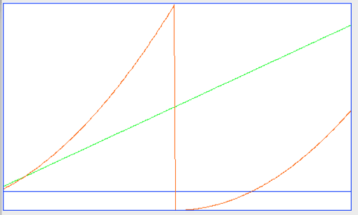
The stack pointer is constant at 5893, which is the bottom of the stack, 5888, incremented five times. At the time SP is copied into HL, we have nothing at 5888, the top byte of the program counter at 5889, lo byte at 5890, then A, H, and L at 5891, 5892, and 5893. The A3035A is transmitting 177 SPS on three channels. It is performing 177 eight-bit multiplies per second. Current consumption is 209 μA.
We implement a self-calibration of the ring oscillator, which works well if we allow a delay of 8 ms before calibration. The calibration puts TCK at 202 ns every time. We move the device identification number into the software, as well as the RF frequency calibration. We enable the timer interrupt and add an interrupt routine that creates a positive pulse on test point register bit zero. We set the interrupt timer to 128 and observe an interrupt period of 3.94 ms, or 129 periods of 32.768 kHz. New working code is Demo_V08.asm.
[23-DEC-20] Jordan reports. We begin modifying the Multiplier_Demo.asm to get data besides the sensor timer data. The first register we attempt to read data from is the gyroscope temperature register. This is a 16 bit temperature register. This does not work initially, we see a constant transmitted value. The current consumption by the circuit upon power up indicates that it is not in its normal power mode, without normal power mode we cannot read out temperature. We send a normal power mode command data to the CMD register. Upon reprograming we see that the current consumption is around 900 μA, according to the data sheet the normal mode consumes 800 μA. We are also able now to view temperature changes in the recorder instrument. Using a heat gun and cold spray we were able to see the temperature move up and down accordingly. We noticed however, when the A3035AV1 board is unplugged and plugged back in the board does not return to normal mode. We implement a delay of 110 clock cycles to the front of the assembly code. With this delay the device returns to normal mode an transmits properly. We continue to reduce the delay until we determine that the minimum delay needed is one clock cycle. With this delay we can unplug and plug the device in and still have the board return to normal mode. We successfully retrieve X, Y, and Z gyroscope data from the circuit in normal mode. We send commands to the gyr_range register and are able to control the resolution of the gyroscope data and toggle between different range settings. We are able to see X, Y, and Z data simultaneously and take a screenshot of the recorder instrument window while wiggling the A3035AV1 board.
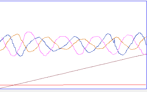
[11-JAN-21] We obtain XYZ axis data from both the gyroscope and accelerometer simultaneously. The current consumption while both sensors are initialized and sending data is 900 μA. We were also able to measure gravitational acceleration by placing the accelerometer flat against the benchtop surface in each axis direction. If the accelerometer is initialized and the gyroscope is not the circuit consumes 190 μA. The accelerometer is configured into its low power mode.
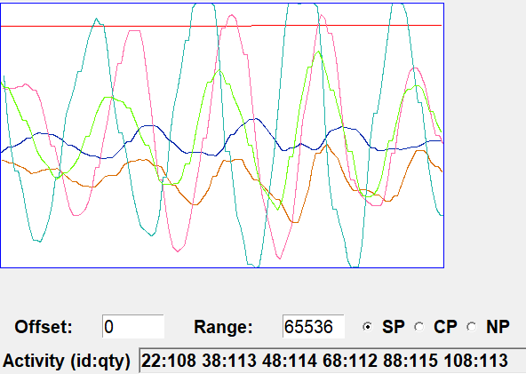
We solder leads to the charging inputs C+ and C− on a new A3035AV1 assembly, add a helical antenna, and load an ML920 battery. We program with the latest code. We connect 4.2 V to the charging inputs through an ammeter, and turn the circuit off. The current flowing into the circuit is around 1 mA, and all but 1 μA of this is flowing into the battery. After ten minutes, current is 0.5 mA and battery voltage is 2.7 V. After an hour, 0.25 mA and 2.75 V. We can turn the circuit on and off so long as the 4.2 V is connected to the charging leads.
[15-JAN-21] We isolate a confusing problem with the gyroscope configuration: the existing configuration routine must be run twice in order for it to succeed. After running it twice, we have three-axis gyroscope at 214 SPS, with interrupt running in background every 7.8 ms, current consumption 1.023 mA. The board will power up off a 1000-mAhr lithium battery but not a 48-mAhr lithium battery. We wiggle it as fast as we can, and see the gyroscope measurement almost, but not quite, reach its limits. Code is gyro_demo_v2.asm.
[18-JAN-21] We now have a gyroscope demonstration program that does not have to call its configuration routine twice, gyro_demo_v3.asm.
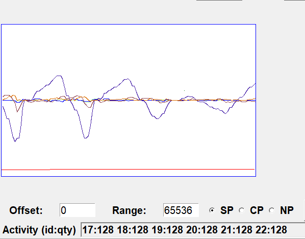
[20-JAN-21] The A303501A board is now transmitting X, Y, and Z axis data from the gyroscope and accelerometer at a rate of 128 SPS. It draws 1.2 mA. We have mounted batteries and antennae on 4 boards and programmed them. They transmit data at 128 SPS. The A303501A needs to be plugged into a external power supply in order to be turned on. Once turned on they can transmit data with just the battery. We will be testing whether the data recorded by the sensors is accurate. We also were able to receive acceleration data without writing the 6-kByte initialization file to the accelerometer.
[22-JAN-21] We fix some bugs in our six-axis code, and we are now transmitting exactly 128 SPS with the CPU running in boost mode in an interrupt in gyro_acc_demo_v4.asm. We are recharging our ML920 batteries by connecting 2.7 V directly to the battery with P2. If we put a resistor in series we cannot start the logic chip. The ML920 has specified capacity of 11 mAhr for a 32-μA drain. When powering our 1.2-mA load, after recharging with 2.7 V, the circuit runs for only half an hour. We have connected LiPo batteries to the A3035AV1 circuit several times by accident, and they have suffered no harm. We connect 4.2 V to the circuit through an ammeter and find the current is 1.15 mA. At 3.7 V, still 1.15 mA. The circuit is running, but reception is poor. The transmit center-frequency is around 925 MHz. We drop the tx_frequency calibration constant from 5 to 4 and we now get robust reception with center-frequency 918 MHz. We leave the circuit running for the weekend off a 150-mAhr LiPo. The 3.7-V LiPo voltage exceeds the absolute maximum voltage for the logic chip's I/O banks (U6, 3.5 V) and the 32.768 kHz oscillator (U4, 3.6 V), but not that of the gyroscope (U8, 4.25 V), accelerometer (U7, 4.0 V), RF VCO (6.0 V), magnetic sensor (U1, 7.0 V) or flip-flop (U2, 4.6 V). The A3035AV1 circuit will run a lipo battery down to 1.2 V if left running or left on the shelf for months. So we must turn it off and re-charge it before the battery gets below 3.0 V, or the battery will lose capacity.
[23-JAN-21] Our A3035AV1 is still running off our big lipo battery. Current consumption 1.15 mA, battery voltage is 3.88 V. Reception 100%.
[26-JAN-21] We record from an A3035A spinning on a horizontal wheel for 85 s. The wheel spins with a motor. We adjust the motor power, at one point turning it off completely so it slows to a stop. Gyroscope and accelerometer measurements agree with one another in proportion to radius circuit orientation. See M1611675170.ndf.

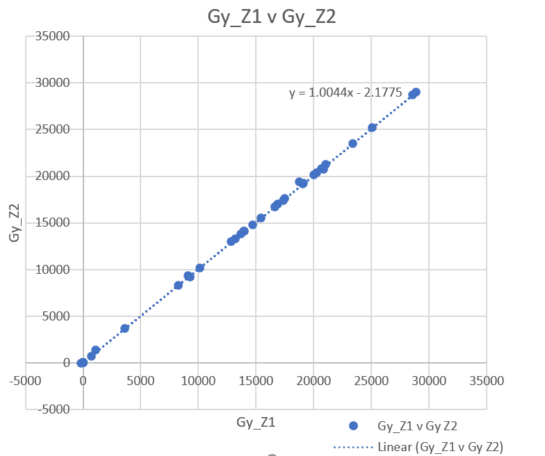
[29-JAN-21] We mount two A3035A on our spinning wheel with gyroscope z-axis vertical and accelerometer x-axis radial. One we place at a smaller radius with its x-axis facing away from the axis of rotation, and the other at a greater radius with its x-axis facing towards the axis of rotation. We vary speed and record all six measurements from both devices for 100 s.

The gyroscope measurements of rotation about z are so similar that one obscures the other in the plot above. The acceleration of the more distant device is positive and greater in magnitude than the negative acceleration of the other device by a factor equal to the ratio or radii within 5%. We plot the two gyroscope measurements of angular velocity against one another below.
[01-FEB-21] We set up a pendulum of length 146 cm, the period of which should be 2.42 s using 2π√(l/g), where l = 1.46 m and g = 9.81 m/s/s. We attach A3035A No17 to the pendulum, with its gyroscope x-axis vertical and the accelerometer y-axis parallel to the pendulum string. Rotation about the string is not well-controlled. The other two axis directions settle at around 45° to the pendulum movement.

The oscillations we record do indeed show a period of 2.4 s. The gyroscope x rotation shows the pendulum weight rotating and unrotating about the axis of the string.
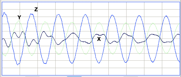
The accelerometer y-measurement has a peak in its frequency spectrum at a period 1.2 s, which is double the period of the pendulum. We resolve to re-arrange the sensor axes so the accelerometer and gyroscope have their x, y, and z coordinates in the same direction, even if we have to negate the sensor values before we add an offset and transmit.
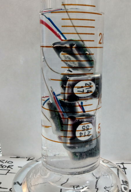
[12-FEB-21] We have five A3035A encapsulated in epoxy and silicone. We measure their displacement volume: 5 ml for 5 devices is 1.0 ml each.
[15-FEB-21] The A3035A microprocessor code is C3035AV1.asm. This code does not provide transmit scatter, so two devices colliding in the same enclosure could cause 100% signal loss.
[06-APR-22] Update the memory map to suit the V11 firmware. We are using P3035A11_Main.vhd as the basis for our new Implantable Stimulator-Transponder firmware P3041/Main.vhd.
| Address (hex) | Read/ Write | Function |
|---|---|---|
| 0000 | R/W | Program Variable Memory and Configuration Data (6 KB = 6144 Bytes) |
| 1700 | R/W | Bottom of Program Stack (SP = 5888) |
| 17FF | R/W | Top of Program Stack (SP = 6143) |
| 1E00 | R/W | Sensor Data Hi Byte (D0-D7 give SD8-SD15) |
| 1E01 | R/W | Sensor Data Lo Byte (D0-D7 give SD0-SD7) |
| 1E02 | W | Sensor Register Location (D0-D6 give SA0-SA6) |
| 1E04 | W | Sensor Control Register (write initiates access, D0-D2 are GYSEL, SAWR, SA16) |
| 1E10 | R | Interrupt Request Bits (D0-D7: TMR, TXD, SAD, INTG, INTA, GPI1-3) |
| 1E12 | R/W | Interrupt Mask Bits (store "1" to Dn to enable interrupt n) |
| 1E14 | W | Interrupt Reset Bits (write "1" to Dn to clear interrupt n) |
| 1E16 | W | Interrupt Set Bits (write "1" to Dn to set interrupt n) |
| 1E18 | R/W | Interrupt Timer Period (multiple of RCK period = 30.52 μs) |
| 1E19 | W | System Reset (D0 is SWRST) |
| 1E20 | W | Transmit Hi Byte (D0-D7 are TD8-TD15) |
| 1E21 | W | Transmit Lo Byte (D0-D7 are TD0-TD7) |
| 1E22 | W | Transmit Channel Offset (channel = device_id + offset) |
| 1E24 | W | Transmit Control Register (any write initiates transmission) |
| 1E26 | W | Transmit Frequency Calibration (sets zero-bit frequency for transmitter) |
| 1E30 | W | Enable Transmit Clock (D0 is ENTCK) |
| 1E32 | R | Transmit Clock Frequency (0-255, multiple of RCK = 32.768 kHz) |
| 1E34 | W | Transmit Clock Divider (0-15, divides ring oscillator to get TCK) |
| 1E36 | W | Boost CPU Clock (D0 is BOOST) |
| 1E38 | W | Test Point Register (D0-D7 are CPUTP0-CPUTP7) |
| 1E39 | W | Test Point Register (D0-D7 are CPUTP0-CPUTP7) |
| 1E3A | W | Multiplier Input A |
| 1E3B | W | Multiplier Input B |
| 1E3C | R | Multiplier Output HI |
| 1E3D | R | Multiplier Output LO |
[09-APR-22] We touch the pins of P2 with a CR1025 battery so as to connect the battery to VB. We repeatedly power up the A3035A with the tiny battery. We are trying out the new OSR8V2 with the P3035A12 code. While programming, we confirm that we have to attempt to program twice every time. The first time seems to set up the device for the second time, when the programming takes place. Or we can disconnect and reconnect power, and program first time.
[11-APR-22] We upgrade to Lattice Diamond 3.12 and find a number of compiler bugs are resolved. We find a problem in the interrupt handler, whereby a delayed signal is not delayed because the compiler is confused over the implementation of our boost clock. We resolve by clocking the interrupt timer off the negative edge of RCK. Now we have OSR8V3 implemented and we change the stack location, RAM size, I/O locations, and program size, all using the OSR8V3's size constants. Rearrange test points to show test point registers. Code is P3035A12.
[15-JUL-22] We retire all rechargeable versions of the A3035, vowing to manufacture only non-rechargeable versions with CR-series lithium primary batteries. We are about to make a few A3035Bs for photographing. We are offering the IIS with non-rechargeable battery for sale at half the price of our SCT implants because they have no amplifiers to suffer from corrosion damage, nor external leads that we have to stow during encapsulation. We assemble the first A3035B circuit, mounting the battery in the notch on the circuit board, spot-welding two tabs. We observe the battery voltage drops from 2.65 V to 2.50 V during transmission of six messages in 80 μs. Each message transmit drops the voltage by 25 mV. Battery voltage takes 500 μs to recover thereafter.
Create P3035 GitHub repository. Our firmware will reside here from now on.
[25-JUL-22] We discover that the acceleration with respect to the three coordinates is negated. That is, when the device is accelerating in the x-direction, the reported acceleration is negative. Our No87 prototype suffers from this problem, but we update the firmware, reversing the direction of all three accelerometer measurements. Firmware v2.2 incorporates the correction. We consider adding an eight-bit ADC to the A3035 circuit, and begin looking at A303501B, but decide that adding up operating time automatically using the Neuroplayer is a better way to keep track of battery capacity.
[08-FEB-24] Discontinue previous versions that used LiPo batteries. The LiPo batteries swell up when discharged, lose capacity if allowed to discharge completely, and require the customer to recharge frequently, in which process our customers often connect the battery in the wrong way, leading to failed recharging and failed experiments. Instead, decide to power the A3035 only with CR-series lithium primary coin cells. The A3035A2 circuit requires a 1.5-ms pulse of 10 mA at startup, and 1.2 mA thereafter. We found in our work with the A3041 that pulsed currents and high drain currents are not tolerated well by batteries made by Renata or Panasonic. Those made by Murata, however, have specified and superb performance under pulsed loads and high loads. Create and assign new version letters and sample rate codes for versions using CR-series coin cells from Murata. Discontinue devices that use the CR1225, which is not available from Murata.
[21-JUN-24] The Multicomp CR1225 battery provides excellent pulsed performance as well as capacity. We add the A3035B1 to our Version Table, an accelerometer-only, 128 SPS IIS equipped with this new battery.
[24-JUN-24] We start on P3035 V1.4, in which we can enable and disable the gyroscope. We make the accelerometer channels the first three channels always, with the gyroscope channels following. Current consumption of the A3035A2, with 128 SPS from both accelerometer and gyroscope, is 1.15 mA. We put the gyroscope into suspend mode, but keep transmitting its samples, current is 330 μA. When we stop the 384 SPS from the gyroscope, current is 280 μA. Current per SPS is around 0.13 μA. We turn off averaging and filtering, we reduce update rate to 100 Hz, current drops to 258 μA. Reduce update rate to 25 Hz, 248 μA. Ten minutes, later, 234 μA. Warm with fingers, back to 250 μA. Reprogram, disabling the accelerometer, 235 μA. Return to 100 Hz update, 261 μA. We consult our measurements of LCMXO2-1200 in the WLCSP-25 and TQFP-100 packages in 06JAN20 and in 05SEP23. One WLCSP-25 chips we purchased in 2020 consumed 170 μA at 25 °C, compared to 100 μA for the chips we purchased in 2023. Given that our A3035 circuits were made in 2020, we suspect that newer logic chips would drop current consumption by 70 μA at room temperature.
[25-JUN-24] Our A3035B1 transmits 128 SPS of x, y, and z acceleration. At room temperature, it consumes 258 μA. We apply freezer spray and see current consumption drop to 106 μA. Of this, 50 μA is transmission. Consulting the BMA423 data sheet, we expect the accelerometer to consume 25 μA at 100-Hz update rate. In which case, the logic chip is consuming around 30 μA at −40°C, which is consistent with 06JAN20. Warm up with heat gun, 800 μA. Cool down to room temperature, 255 μA. At 37°C we expect another 50 μA, bringing the total while implanted in a mouse to around 310 μA. With battery capacity 48 mAhr, operating life is 150 hrs implanted. Our newer WLCSP-25 LCMXO2-1200ZE chips consume 100 μA at 25°C, see 05SEP23. With newer logic chips we expect current consumption of the A3035B1 to be only 170 μA at 37°C. Operating life with 48 mAhr battery will be 280 hrs.
The program running in the A3035 microprocessor is so simple, we believe we can replace it with state machines. If so, we can move to the LCMXO2-256ZE, with 256 LUTs, no RAM, and quiescent current 18μA typical at 25°C, compared to 65μA for the XO2-1200ZE. We might see the current consumption of the logic drop by a factor of 3.6. The A3035B1 might consume only 120 μA for operating life 400 hrs = 17 days.
[27-JUN-24] We have a compact branch of P3035 in which we create the OSM8, a mini version of the OSR8, with 128-byte program memory, 16-byte RAM, and 256-byte CPU address space. We eliminate half the instructions, eliminate the stack, interrupts, and subroutine calls. We add "ex A,B" and leave all the arithmetic routines in place. The resulting code size drops from 1201 to 432 LUTs, which is still too large to fit in the LCMXO2-256. Return to master and add "ex A,B" instruction to OSR8. Code size increases from 1201 LUT to 1225 LUT. Remove the exchange instruction: we can achieve the same result with "push A; push B; pop A; pop B".
[27-SEP-24] We prepare three of A3035B1. Our control over the RF center frequency is crude: increasing tx_frequency from 4 to 5 raises the center frequency by 10 MHz. Our frequency step between LO and HI frequency is one count, so our modulation width is 10 MHz. Active current consumptions at room temperature are 199, 184, and 258 μA for No1, No4, and No7 respectively.
[03-OCT-24] We have three of A3035B1 encapsulated. Average mass 1.78 g. The antennas stick straight out. By removing the circuit's recharging diodes, we could have made it possible to attach the antenna one both ends, but we wanted to see what our customer, who is receiving two as samples, things of the straight antenna.