| Diameter | Voltage | Length | Shape |
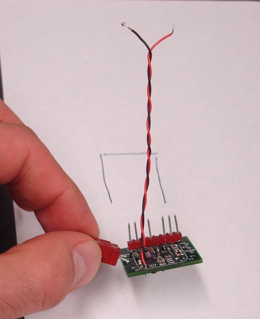
[21-JAN-10] The Subcutaneous Transmitter (A3013) transmits biometric signals from within the body of a live animal. It is the implantable transmitter component of our Subcutaneous Transmitter System. The A3013 detects biometric signals with flexible 150-mm leads, digitizes them, and transmits them as bursts of 915-MHz radio-frequency power through a 50-mm antenna. A nearby antenna receives the radio-frequency bursts and records the biometric signals. Within a faraday enclosure, such as our FE2A, the operating range of the A3013 is limited only by the size of the enclosure. Without a faraday enclosure, operating range varies from 25 cm on the eighth floor of an office building in London to 200 cm in a basement laboratory in Boston. We designed the A3013 to monitor EEG in rats.

The A3013A transmits 512 samples per second for over nine weeks before its battery runs out. We can turn the transmitter on and off at any time with a magnet, even when the transmitter is implanted in an animal. When turned off, the transmitter will run its battery down in thirty-two weeks. (See Battery Life for more details.)
| Property | Value |
|---|---|
| Volume (without leads) | 2.4 ml |
| Volume (with leads) | 2.9 ml |
| Operating Life | >8 wks |
| Shelf Life | 32 wks |
| Number of Inputs | 1 |
| Type of Input | Differential |
| Input Impedance | 10 MΩ || 2 pF |
| Samples Per Second | 512 |
| Sample Resolution | 16-bit |
| Input Dynamic Range | 9 mV |
| Input Bandwidth | 0.2 Hz − 160 Hz |
| Input Noise | 12 μV |
| Input Mains Hum | <1 μV |
The A3013 is encapsulated in epoxy and coated with silicone. The resulting encapsulation is inert, water-proof, resistant to vacuum, easy to clean, tough enough to survive unharmed inside an animal for nine weeks, and tolerant of temperatures from −40°C to +125°C. Once the battery is exhausted, however, the transmitter must be discarded. There is no way to break open the epoxy encapsulation to replace the battery. (See Encapsulation for more details.)
Because the A3013 is battery-powered, it provides perfect differential reception for its first input with only two wires. The A3013A has a single analog input, which takes the form of a two-wire, differential 10-MΩ input impedance. The input's dynamic range is 9 mV. A one-pole high-pass filter and a three-pole low-pass filter provide a bandwidth of 0.2 Hz to 160 Hz. Within this bandwidth the electrical noise on the input is 12 μV, which is 80 of the transmitter's sixteen-bit ADC counts. (See Analog Inputs for more details.)
The A3013's radio-frequency transmissions occupy most of the bandwidth available in the 902−928 MHz ISM Band. Multiple A3013's operating in the same area can share the same receiving antenna. The A3013 radio-frequency transmissions are so brief that collisions between transmitters are rare. When collisions do occur, the data acquisition system eliminates the corrupted measurements from the data stream. The resulting degradation in signal quality is minimal. Eight A3013s can share the same receiving antenna and all maintain a signal bandwidth of 160 Hz simultaneously. If we drop the signal bandwidth to 40 Hz, forty transmitters could share the same antenna. (See the Collisions section of Subcutaneous Transmitters.)
The A3013 uses stainless steel springs for its analog leads, and stranded stainless steel cable for its antenna. All are insulated in silicone. The leads and antenna are designed to survive in a live animal for several months, where wires are subject to millions of repetetive stress cycles in both tension, torsion, and compression. (See Subcutaneous Leads for more details.)
All versions of the A3013 start off with a programming extension that allows us to program the transmitter's logic chip, calibrate its radio frequencies, and set its channel number and sample rate.

The A3013 provides one or two inputs, depending upon how it has been programmed. On the A3013A and A3013B, channel X is fully-differential with dynamic range 9 mV, input impedance 10 MΩ, bandwidth 0.2 Hz to 160 Hz, and noise 12 μV rms. Channel X requires only two connections for a fully-differential measurement because the A3013 is battery-powered, which means its ground potential is floating. On the A3013B, channel Y is single-ended with dynamic range 54 mV, input impedance 10 MΩ, bandwidth 0.2 Hz to 20 Hz, and noise 25 μV. The Y channel has two connections, but we use only the Y+ connection in a live animal. The A3013B records the potential of Y+ compared to X−.
| Name | Function | Comment |
|---|---|---|
| X+ | X signal input | connected to 100 nF and 10 MΩ |
| X− | X ground input | connected to VCOM |
| Antenna | radio-frequency antenna | a flexible wire |
| Y+ | Y signal input | connected to 100 nF and 10 MΩ |
| Y− | Y ground input, unused in animals | connected to VCOM |
The A3013C transmits both channels at 64 SPS, for a combined transmission rate of 128 SPS. Other dual-channel transmitters skip an occasional sample from X for a sample of Y. The A3013B, skips every eighth sample X for a sample of Y. Channel X receives 448 SPS, with the samples un-equally spaced, while channel Y receives 64 SPS equally-spaced samples. Dual-channel transmitters give each channel its own channel number in the messages they transmit. The receiver will record the two channels as if they were transmitted from two separate transmitters.
The sample rate and battery life of an A3013 varies from one version to another. The A3013A, for example, transmits 512 samples per second from a single channel, and will operate continuously for at least two months. The A3013C, on the other hand, transmits 64 samples per second from each of two channels, and will operate continuously for five months. When de-activated, all versions of the A3013 have battery life nine months. As you use up this nine months, the operating life is used up in proportion. After four and a half months on the shelf, an A3013A will have operating life four and a half weeks.
We receive A3013 transmissions with our Data Receiver (A3018). The Data Receiver stores the signal it receives from one or more Subcutaneous Transmitters. Each transmitter uses a different channel number to distinguish its transmissions from those of other transmitters. The transmitters share the same radio frequency band by each transmitting for only a tiny fraction of the time. We read out and display the transmitter signals with our Receiver Instrument. We analyze and store the signals with our Neuroarchiver Tool.
The A3013 is an improved version of the Subcutaneous Transmitter (A3009). See the A3009 manual for most of our work on the core circuits of the A3013. In the passages below, you will fine an account of our development and testing of the A3013, along with graphs and tables of its performance and specifications.
Note: All our schematics and Gerber files are distributed for free under the GNU General Public License.
S3013_1: Logic chip, 900-MHz oscillator, battery, reference clock, antenna, analog inputs, anti-aliasing filters, sixteen-bit ADC, and amplifiers. Component values shown are for the A3013A.
S3013_2: Programming extension.
S3013X_1: The A3013X circuit, showing combined antenna and X+ connection with inductors acting as radio-frequency chokes. These inductors caused us problems.
P3013A: Firmware for logic chip of A3013A. Same firmware, with some constant changes, works in all other versions of the transmitter.
A3013A: Assembly spreadsheet for A3013A, including BOM, KIT, and COST.
A301301A: Printed circuit board files in zip archive.
Panel Drawing: Drawing of 6 × 2 panel.
Panel Files: Gerber files for 6 × 2 panel.
[21-JAN-10] An A3013 part number has the form A3013f-p, where f is the transmitter function code and p is the transmitter packaging code. The function code specifies the behavior of the two input channels. The packaging code specifies the physical encapsulation or lack of encapsulation.
| Function Code |
X | Y | Operating Life (weeks) |
Shelf Life (weeks) |
|---|---|---|---|---|
| X | Antenna and X+ share same wire. | None | 9.6 | 32 |
| A | ×300, 9-mV range, 0.2-Hz HPF, 160-Hz 3-pole LPF, 512 SPS |
None | 9.6 | 32 |
| B | ×300, 9-mV range, 0.2-Hz HPF, 160-Hz 3-pole LPF, 448 SPS |
×50, 54-mV range, 0.2-Hz HPF, 20-Hz 1-pole LPF, 64 SPS |
9.6 | 32 |
| C | ×300, 9-mV range, 0.2-Hz HPF, 20-Hz 3-pole LPF, 64 SPS |
×50, 54-mV range, 0.2-Hz HPF, 20-Hz 1-pole LPF, 64 SPS |
20 | 32 |
| D | ×300, 9-mV range, 0.2-Hz HPF, 80-Hz 3-pole LPF, 256 SPS |
×50, 54-mV range, 0.2-Hz HPF, 20-Hz 1-pole LPF, 256 SPS |
9.6 | 32 |
| E | ×300, 9-mV range, 0.2-Hz HPF, 320-Hz 3-pole LPF, 1024 SPS |
None | 5.7 | 32 |
| H | ×300, 9-mV range, 0.2-Hz HPF, 32-Hz 3-pole LPF, 128 SPS |
None | 20 | 32 |
| L | ×300, 9-mV range, 0.2-Hz HPF, 160-Hz 3-pole LPF, 512 SPS, 1 s transmission every 10 s. |
None | 32 | 32 |
| R | Artificial square wave, 512 SPS | None | 9.6 | 32 |
We set the function of a transmitter during assembly and programming. We change cacitors on the board to set filter frequencies. We change resistors to set the channel gains. We program the logic chip to set the sample frequency for each channel.
The A3013B transmits 512 messages per second, and shares these between two channels. It transmits seven messages in a row from X and then transmits one from Y. The result is 64 SPS for Y, and 448 SPS for X, but the X-samples are not regular. We can do this, and still maintain near-perfect 160-Hz bandwidth, because our data acquisition software will insert a substitute message in place of the missing message, and give this message the same sample value as the previous message it received from channel X. This substitution, combined with the sharp roll-off of our channel-X low-pass filter, give us near-perfect reconstruction of the original signal.
The A3013L is an intermittent transmitter. It transmits at 512 SPS with 160-Hz bandwidth for 1 s each minute, in order to give a snapshot of a signal once a minute for 32 weeks.
| Packaging Code | Description | |||||
|---|---|---|---|---|---|---|
| E | encapsulated with epoxy and silicone | |||||
| N | naked circuit with battery, insulated leads and insulated antenna, but without programming extension | |||||
| P | naked circuit with programming extension and uninsulated antenna, but no leads |
| Transmitter | Inactive Consumption (μA) | Active Consumption (μA) |
|---|---|---|
| 1 | 18 | 76 |
| 2 | 21 | 77 |
| 3 | 17 | 84 |
The active current consumption of the A3009 was higher by roughly 15 μ. The A3009 had many problems with erratic current consumption as a result of our over-heating its BGA logic chip during assembly. We have observed no such effects in the A3013, nor do we expect to. The A3013 uses a TQFP package instead of a BGA, and we have long experience soldering TQFP packages. For more current consumption measurements see below.
The ADC on an A3013A broke. This was while we were experimenting with 2.5 MBPS messages. The message duration increases from 7 μs to 12 μs when we drop from our usual 5 MBPS down to 2.5 MBPS, so the message-transmission component of the active current consumption almost doubled. While we pulled parts off the board trying to find out which one was broken, we measured the current consumption of the circuit in various states.
| State | Consumption (μA) |
|---|---|
| No U1, U2, U3 or U5 | 4.1 |
| Restore U1 | 6.1 |
| Restore U2, inactive | 18.6 |
| Restore U5, inactive | 19.0 |
| Activate | 63.5 |
| Restore U3, inactive | 17.8 |
| Activate | 108 |
As you can see, the inactive current remains unchanged at the lower bit rate, but the active current increases by roughly 35%. The battery life would therefore be 35% shorter. See here for a comparison of the two bit rates.
From the above results, we conclude that the current consumption of an A3013 transmitting at bit rate 5 MBPS is roughly 20 μA + 120 nA/SPS. AT 512 SPS, that's 80 μA, and at 128 SPS, it's 35 μA.
[10-SEP-09] We now have inactive and active current consumption for sixty A3013A transmitters, which you will find in this Excel spreadsheet. The average active current consumption is 74 μA, with a standard deviation of 2.4 μA. The average inactive current consumption is 22 μA, with a standard deviation of 2.0 μA. All versions of the A3013 will have the same inactive current consumption. An A3013 that transmits M messages per second will have expected active current consumption:
Iactive = Iinactive + (M × 0.10 μA)
We use this formula to obtain the expected battery life for each version of A3013 in the table above. We present our measurements of actual battery life below.
[21-JAN-10] The A3013A's BR1632 battery has guaranteed capacity 120 mA-hr. The following plot shows how the battery voltage varies with time for four transmitters.

The following table gives initial active current consumption as measured before the test, the battery life, and the final active current consumption, as measured with a fresh battery after the test.
| Transmitter | Initial Current (μA) |
Battery Life (hrs) |
Final Current (μA) |
Calculated Capacity (mA-hr) |
|---|---|---|---|---|
| 7.56 | 83 | 1510 | 83.4 | 126 |
| 8.57 | 72 | 1820 | 74.5 | 136 |
| 9.58 | 72 | 1480 | 74.3 | 110 |
| 10.59 | 72 | 1780 | 74.8 | 133 |
Battery life does not correlate well with the current consumption. The current consumption itself appears to have risen slightly during the experiment, but this may be due to a change in the meter we used to measure the currents the second time. All batteries were at the same temperature throughout the experiment. We conclude that the battery capacity of our BR1632 batteries vary from one device to the next. If we multiply active current by lifetime, we arrive at the capacities given in the final column. The manufacturer's value for "nominal" capacity is 120 mA-hr.
We we confirmed the BR1632 capacity in our study of the A3009's battery life. We discuss current consumption in the section above. The A3013A's active current consumption is around 74 μA. We expect its operating life to be around nine and a half weeks. It's inactive current consumption is around 22 μmA. We expect its shelf life to be around thirty-two weeks. We present the expected battery life of various versions of the A3013 in the table above. Here is a history of our measurement of battery life, starting with our earliest measurements.
[03-MAR-08] For the past few weeks we have been running an A3013A, channel number 5, from a near-exhausted battery. Today the average X input is 52300, indicating a battery voltage of 2.26 V (65535 counts is VBAT and the average of X is 1.8 V). We measure the battery voltage directly with a voltmeter and found it to be 2.27 V. This tells us that the average value of X is a good measurement of VBAT even as we near failure, and that the circuit works down to at least 2.27 V. (Raw data here.)
[05-MAR-08] Transmitter is still working. Reception is robust at range 100 cm. Average X is 56533, indicating VBAT = 2.09 V. (Raw data here.) We observe reception of 60-Hz hum, and step changes when we touch the electrodes. (Raw data here.)
[11-MAR-08] Transmitter 5 has stopped transmitting. Battery voltage is 1.6 V. We give it a new battery of a new type: the CR2032, which is 20 mm in diameter and has a capacity of 225 mA-hr. Our usual battery is the BF1632, a 16-mm diameter battery with 120 mA-hr capacity. We start recording once per hour to see how long the battery will last. This A3013A is one of our rejects. It's quiescent current is 95 μA (15 μA higher than our expected 80 μA). We expect the A3013A to run continuously for 225 mA-hr ÷ 95 μA = 2400 hrs.
[24-APR-08] The transmitter has been running continuously for 1000 hours. We see the battery voltage drop from 2.98 V to 2.86 V in the first few hours of operation. Since then the battery voltage has climbed slowly to 2.90 V. We reduce our recording rate to once per day.
[13-JUN-08] At 2300 hrs, battery voltage has dropped to 2.4 V. Our expected battery life is 2400 hrs. The transmitter is still functioning.
[25-JUN-08] The transmitter failed at 2425 hrs. We are now confident that we understand how to relate battery capacity to transmitter operating life.
[03-SEP-08] We took out a A3013D-N transmitter (two channels with 256 samples per second) that received a new battery on 27-DEC-07. Nine months have passed since the new battery was installed, and for that time the transmitter has been inactive. We turned it on and received 100% reliable transmission with no transmitting antenna when the transmitter was 5 cm from the receiving antenna. The channel noise was 100 counts on X and 20 counts on Y. The average value was 47871 on X and 46312 on Y. From this we deduce that the battery voltage is 2.47 V, which means the battery is 90% exhausted. We see that the shelf life of an A3013 is roughly 10 months, with a 10% loss of battery life every month.
[01-OCT-08] The A3013D-N still works when we turn it on. The average value was 60500 on X and 57700 on Y, suggesting a battery voltage of 1.95 V. With a voltmeter we measure 2.08 V.
[04-SEP-09] An A3013A-E operated at ION for one week outside an animal followed by seven weeks inside an animal before it's battery failed. The transmitter was inactive for at least two weeks prior to its use at ION. One week before failure, the battery voltage was 2.5 V. On the day of failure, reception from the transmitter remained good, but the X value was stuck at zero.
[10-SEP-09] We ran an A3013A-E in a jar of saltwater, operating continuously since 08-JUL-09. On 09-SEP-09 its battery voltage was 2.2 V. Today reception is good, but X is stuck at zero. The transmitter operated for a total of 9.6 weeks, which matches our expected battery life.
[14-SEP-09] The transmitter in a jar of saltwater has now stopped transmitting altogether. We place four A3013A transmitters in a faraday enclosure with fresh batteries.
[13-JUL-11] We obtain a graph of VBAT versus time for the entire life of a battery in an A3013A, so confirm that the final version of the circuit, and the latest batteries, are consistent with the originals. You can view the graph here. The result is consistent.
[21-JAN-10] The ADC (U5 in the schematic, an LTC1865) converts either its X or Y input into a 16-bit number. A 16-bit count of 0 means an input voltage of 0V. A count of 65535 means a voltage equal to the 3VA supply, which we call VBAT in this manual. The VBAT voltage starts off at about 2.7 V when the battery is fresh, and drops to about 2.2 V just before the transmitter fails. As you can see from this graph, the battery voltage drops quickly in the last few days of the transmitters life, but up until that time remains approximately steady at 2.7 V. We assume a battery voltage of 2.7 V when we calculate the analog input dynamic range, but we do not claim that the absolute values returned by the transmitter are an accurate measure of the absolute applied voltage on a time-scale of days or weeks.
The dynamic range of either input channel is 2.7 V divided by the channel gain. In the case of channel X in the A3013A or A3013B, the dynamic range is 2.7 V / 300 = 9 mV. Each ADC count represents a 140-nV change in X. The dynamic range of Y in the A3013B is 2.7 V / 50 = 54 mV (the A3013A does not provide a Y channel). Each ADC count represents an 820-nV change in Y.
When we short the inputs of an A3013A together, we observe noise of standard deviation 70 ADC counts. This 70 ADC represents is 10 μV rms noise at the X input. If we remove R12 in the schematic, we see noise of 12 ADC counts, which means the 10 μV is indeed arising at the X input. The thermal noise generated by a 10-MΩ resistor in the 160-Hz pass-band of the A3013A is 5 μV. Our input noise is twice the theoretical minimum possible with a 10-MΩ signal source. With this we are well-satisfied.
But it is clear that our input noise is not generated by resistors. The inputs are shorted together, and the only remaining resistor on the input of the amplifier (U6 in the schematic) is R10, 200 kΩ. The thermal noise at the input should be less than 1 μV. What we are seeing in our 70 counts of input noise is the noise generated by U6, an OPA2349. The OPA2349 data sheet specifies a typical input noise of 8 μV p-p noise in the 0.1 Hz to 10 Hz range (that's pink noise, or 1/f noise), and 300 nV/√Hz above 10 Hz (that's white noise). In terms of ADC counts, we can expect 60-count fluctuations from one second to the next, and 30 counts of white noise. If we look at the input noise, we do see fluctuations combined with white noise, and the combination amounts to anything from 60 counts in one transmitter, to 100 counts in another. We also observe the size of the noise to vary with time in a single transmitter.
We conclude that our circuit-generated noise is dominated by that of our input amplifier, and that this noise can vary unpredictably with time, and from one transmitter to the next. So far, we have observed input noise varying from 60 to 100 counts when measured over a one-second period.
With 0 V applied to either input, the nomial voltage applied to the ADC input will be 1.8 V, which is VCOM in the schematic. Offsets in the amplifier op-amps can be as large as 10 mV for each stage, so the actual zero-signal voltage applied to the ADC might be higher or lower than 1.8 V, depending upon the final-stage gain. With a gain of 50 in the final stage, as applies for Y in the A3013C, the zero-signal voltage could be as high as 2.3 V and as low as 1.3 V. Because of this, the dynamic range with respect to the zero-signal can be anything from −46mV..+8mV to −26mV..+28mV. For channel X the problem is less severe, because the final-stage gain is 11, not 50. The range can be anything from −5.6mV..+3.3mV to −6.3mV..+2.6mV.
We connected the X input of an A3013X to our function generator through two 10-MΩ resistors. On resistor was in series with each of the ±X inputs, and we obtained attenuation of the function generator output by connecting the ±X inputs with a 1-kΩ resistor. The voltage applied to the X was therefore the function generator voltage divided by 20,000. We applied a 10-Hz sinusoid of varying amplitude to the X input using this arrangement of resistors, and obtained the following results.
| Function Generator Amplitude (V) |
X Amplitude (μV) | ADC Amplitude (ADC Counts RMS) |
|---|---|---|
| 2 | 100 | 544 |
| 1 | 50 | 266 |
| 0.5 | 25 | 157 |
| 0.2 | 10 | 107 |
| 0.1 | 5 | 89 |
| 0.05 | 2.5 | 97 |
| 0.025 | 1.2 | 86 |
| 0.01 | 0.5 | 83 |
| 0 | 0 | 86 |
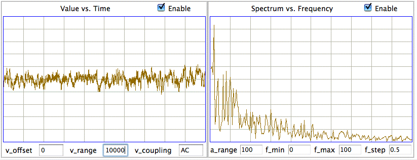
We applied a 10-Hz, 5-μV amplitude input to X and recorded the transmitter for four seconds. The following figure shows the fourier spectrum of the output.
As you can see from the figure, the 10-Hz, 5-μV signal stands out in the fourier spectrum, above the white background noise and mains-frequency (60 Hz) hum. If, however, we gather fewer data points, our 10-Hz signal does not stand out as much. Here is 800 ms of data with a 10-Hz, 10-μV input.
The 10-Hz, 10-μV signal is almost swamped by noise in the signal trace. In the spectrum, the 10-Hz stands out, but is only a few times more powerful than the noise. We conclude that the transmitters sensitivity to a signal depends upon the spectrum of the signal itself and the amount of time for which we can observe it. Given four seconds, the A3013 can detect a 2-μV, 10-Hz signal. Given only 1 second, it can detect only a 10-μV, 10-Hz signal.
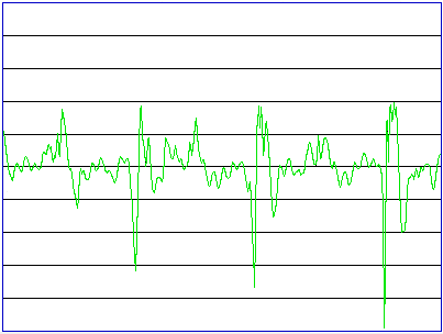
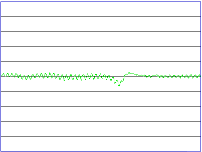
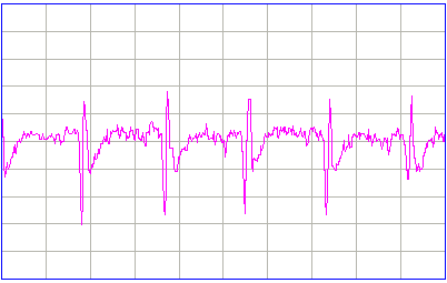
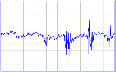
We taped the bare ends of X+ and X− of an A3013B to the chest of a female volunteer. We obtained the trace on the left in the figure below. Our volunteer run up and down the laboratory corridor a few times, and did some jumping jacks. We obtained the trace on the rigth. We conclude that the short spikey features in the recorded signal are her heartbeats.
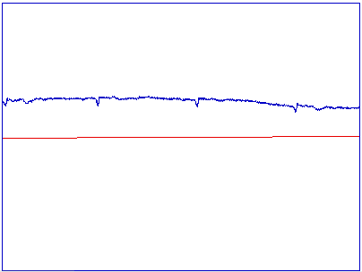
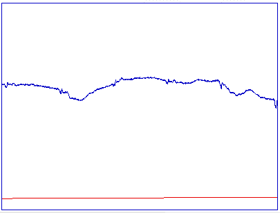
The amplitude of the heartbeat signal is roughly 1000 ADC counts, or 150 μV. In the left trace, our volunteer took slow, shallow breaths, and stood still. In the right trace, she breathed more deeply, and stood less still. We took enough traces to conclude that the low-frequency rumble on the right-hand trace is due to her breathing and movements.
Reception from the transmitter while taped to the volunteer was less robust than when held in free air. We had to keep the transmitter within 1 m of the antenna, and in a favorable orientation, in order to obtain reliable reception. We wrapped tape around the end of X+ to insulate it, to see if connection of X+ to the body was the problem. But reception remained poor. If we move the transmitter itself away from the body, reception improves. The antenna is less efficient when it it lies on a large, flat, conducting body such as the human chest.
The three-pole low-pass filter we use on channel X in the A3013A has a cut-off frequency of 160 Hz. The filter is identical to that of the A3009, whose frequency response we show here. The three-pole low-pass filter we use on channel X in the A3013D has cut-off frequency 80 Hz. The one-pole low-pass filter we use on channel Y in the A3013D has cut-off frequency 20 Hz. We applied a 1-mV amplitude sine wave of varying frequency to X on an A3013A, and then simultaneously to X and Y on an A3013D. We recorded the rms amplitude of the transmitter output in units of ADC counts and obtained the graph shown below.

We tested the analog inputs of our A3013Xs, which used the now-obsolete combined antenna and X+ wire.
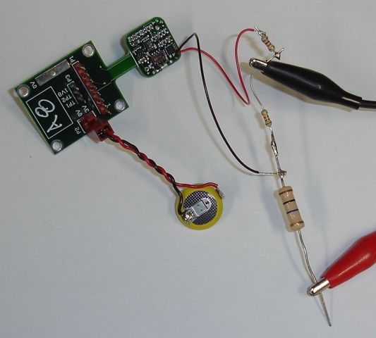
As you can see, the red antenna wire is terminated by a 1-kΩ resistor. We cannot connect the red wire of an A3013X directly to the black or red clip without compromising radio-transmission (see below).
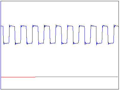
We connected each transmitter to the test apparatus as shown, and applied a 10-Hz, 20-V peak-to-peak square wave to the black and red clips. The signal applied to the transmitter inputs is 2 mV peak-to-peak. We checked that each transmitter produced a waveform like the one below.
We also tried several other inputs on some of the transmitters, to make sure that they met our expectations with noise, gain, and frequency response. We stored the raw Receiver Instrument data for you to look at yourself. To view the raw data, download the file and open it from the Receiver Instrument in LWDAQ. You can look at Noise taken with a 1-kΩ resistor across the X inputs, 2-mV 10-Hz Square Wave, 200-uV 10-Hz Square Wave, and 40-uV 100-Hz Square Wave. If you open the Neuroarchiver, you can look at the spectrum of these waveforms also.
We recorded X overnight from an A2013A. The transmitter was coated with our Process V, immersed in salt-water, with the X wires soldered together. We monitored X in 5-second intervals and recored its average value in each interval as well as its standard deviation.

The average value of X corresponds to VCOM, or 1.8 V. The value of X in ADC counts will rise as the battery voltage, VBAT drops, because X = 65535 × VCOM / VBAT. In this case, X rises by roughly 300 counts in 17 hours, which corresponds to VBAT dropping by roughly 20 mV. The standard deviation of X corresponds to the analog input noise. The standard deviation is almost always 100 counts, which corresponds to 13 μV. But we see spikes in both the average and standard deviation of X. The following graph shows a close-up of such a spike.

Something forces a sudden and temporary jump of 65 μV in X during the night. The jump in X endures for roughly one minute, and then subsides. The standard deviation of X rises during the jump up and the jump down, but otherwise remains close to 100 counts. We are not certain of the causes of these spikes, but we do not obvserve them in the newer A3013A, where the X+ and antenna connections are separated.
For sources of noise inside the A3013 circuit, including thermal noise, see the the section above. Here we discuss external sources of noise. One external source of noise is mains hum. In the USA, mains hum is 60 Hz noise from power cables, and in Europe is 50 Hz noise from the same sources. To understand sources of mains hum, please consult our The Source of Mains Hum.
We measured the mains hum received by channel X of our A3013X for various combinations of wires and resistors across its terminals over a metal optical table (where we found there was a lot of mains hum).
| Load Resistance (kΩ) | Lead Length (mm) | Mains Hum at X (μV rms) |
|---|---|---|
| 1 | 20 | 13 |
| ∞ | 0 | 28 |
| ∞ | 80 | 629 |
| 0 | 80 | 13 |
| 1000 | 80 | 42 |
| 1000 | 80, Shorter Battery Leads | 18 |
The mains hum cannot be induced by magnetic fields, or else the noise would be greatest when the resistance was smallest. The 10 MΩ input resistance of channel X forms a loop with the lead wires, and this loop would pick up and transwer most energy to the 10 MΩ input resistance when there was no other resistance in the loop to compete with it for voltage. We conclude, as we did in The Source of Mains Hum, that mains hum is an electromagnetic wave picked up by the X+ and X− leads. The smaller the resistance across the inputs, the greater the load upon the capacitive impedance that supplies the mains hum, and the smaller the mains hum.

We now took the same transmitter, with 80-mm twisted leads, and placed it over a desk instead of the metal optical table, where there was less mains hum. We measured the mains hum with the transmitter with various loads. We rotated the transmitter about the vertical axis. In each orientation, the wires were straight up, as they are in the figure above, and the transmitter board remained centered above the same spot on the desk.
| Resistance (MΩ) | Orientation (deg) | Mains Hum at X (μV rms) |
|---|---|---|
| 0 | 0 | 12 |
| 1 | 0 | 16 |
| 10 | 0 | 60 |
| ∞ | 0 | 112 |
| ∞ | 45 | 114 |
| ∞ | 90 | 113 |
| ∞ | 135 | 114 |
| ∞ | 180 | 109 |
| ∞ | 225 | 112 |
| ∞ | 270 | 111 |
| ∞ | 315 | 105 |
| ∞ | 360 | 108 |
| ∞ | Wiggle | 766 |
| 0 | Wiggle | 12 |
| ∞ | Hand Nearby | 142 |
Orientation does not appear to affect the amplitude of the mains hum. Holding our hands near the transmitter, and wiggling the transmitter, cause large signals on the input, but these are not mains hum signals. Here is what we see when we wiggle the transmitter and wave our hands near it.
Wiggling the transmitter creates a large signal on X. This signal vanishes when we connect the ends of the input leads with a 1-kΩ resistor. If the signal were caused by magnetic induction, the signal would remain even with a 1-kΩ resistor. Therefore what we are seeing is the movement of the two electrodes through an electrostatic field above the desk. When we move our hands near the electrodes, we create or disturb this field, and so cause interference.
When we leave the transmitter stationary, we see no signal from the electrostatic field because our signal passes immediately through a passive high-pass filter with time constant 100 ms. But we predict that there will be a potential difference between the two electrodes due to the prevailing electrostatic field.
We plan to perform experiments with charged insulting objects moving near open electrodes to confirm our hypothesis. If the source of these signals is indeed electrostatic fields, then we can understand the Delta Power we observed in our mouse earlier. When the mouse moved the electrode wires, which were external to its body, around in the electrostatic field created by rubbing its fur against the cage wall, it generated interference on the electrodes in the 1.5 Hz to 6 Hz band.
If we want to avoid electrostatic noise on our electrodes within an animal, we must make sure that they are enclosed completely by the animals skin. The skin is not a perfect conductor, but we suspect that it conducts well enough to remove electrostatic fields in the region of the electrodes.
[21-JAN-10] We discuss our development of an encapsulation procedure in SCT Encapsulation. Our work is still on-going. At the moment, our favored method is to fill the gap under the battery with silicone caulk and coat four times by dipping in silicone dispersion. We also fill the short piece of heat shrink tube that bundles the wires with caulk before we heat it up, so the space inside the heat shrink is water-tight. We place the heat shrink 10 mm from the transmitter body. The resulting coating is tough on the outside, allows us to wiggle the wires without breaking the coating. In a vacuum, there is so little air trapped within the coating that expanding bubbles do not burst.
[21-JAN-10] Of three transmitters encapsulated with Process X that ION implanted in live animals in February 2008, all failed through wires snapping. In Process X, the wires are soldered to pins that emerge from an epoxy encapsulation. The point at which a wire enters the solder joint is weak because stress concentrates at the point where the effective diameter of the conductor drops from that of the joint to that of the wire. Two silver wires that broke near the animal's skull, but the remaining seven wires broke where the wire emerged from the solder. Among these seven were two silver wires, two tinned, stranded copper wires, and two solid copper wires. We saw no severe corrosion of the wires. We conclude that finding the right wire for long life in an animal will be a project in itself, and we report upon that project in Subcutaneous Leads.
[21-JAN-10] Damage to the RF power source on the A3013 is associated with either complete failure of the RF transmission or by the presense of the battery voltage on the antenna output. We discuss the antenna voltage below. Here we describe our problems with the prototype A3013X, which combined X+ and the antenna, and we describe how even the A3013A antenna connection is vulnerable to damage when we do work upon the antenna wire.
In the A3013X, the X+ wire acts as the RF antenna, as well as the positive input to the X input channel. The red wire will acts as an effective antenna provided you terminate it with a contact resistance of at least 1 kΩ.
In order to share the same wire for both the low-frequency analog X+ input and the radio-frequency output, the A3013X circuits used a 100-nH inductor to isolate the analog input from the antenna wire. This inductor is L1 in the original schematic. Inductors on the outputs of radio-frequency amplifiers can cause oscillations, as we observed here. The first A3013X circuit we made performed well. Chip U3, the radio-frequency oscillator, came from the first of two tubes of MAX2624 chips. But transmitters made using chips from the second tube failed at random. Some of them stopped transmitting altogether. Others introduced noise into the X input.
Before failure, and also after failure in the case of transmitters that produced noise, the operating range of these A3013X transmitters was twice as great as those of transmitters made from chips taken from the first tube. This suggests that the radio-frequency output power had quadrupled. We conclude that the MAX2624 output buffer is near to instability in the presence of L1. Chips from our first tube were stable and operated normally. Chips from the second tube were unstable. They generated four times the rated output power and suffered damage as a result.
One solution to this problem was to use chips only from our second tube. But we decided to eliminate L1 and add a separate antenna wire to the transmitter. It occurred to us that we could fasten this wire to the X wires, and so keep its tip from drifting around inside the animal's body. With the X input wires free of the radio-frequency signal, we can connect them to low-impedance signal sources, which makes them easier to test.
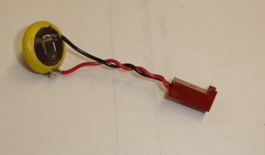
The A3013A has a separate antenna wire, as you can see here. While studying the effect of antenna length and diameter (see below), we discovered that an active transmitter is vulnerable to contact between a metal tool and the antenna wire. We suspect that the RF power source resonates and suffers damage in the same way it did with the inductors present on the A3013X. To avoid damaging the RF power source (that's the MAX2624), we must make sure the transmitter is turned off before we solder the antenna wire or cut the antenna wire.
Making sure that the transmitter is turned off can be a difficult. Our workbench has an asbestos top with a metal backing. The metal backing turns out to be magnetic. Any time we put a transmitter on the bench, there's a chance it will turn on. So we can turn it off, put it on the bench, solder a wire to its antenna output, and find that it is damaged afterwards. The safest way to work on the antenna wire is to do so before we load the battery in place. The Process A encapsulation instructs us to apply all the wires before we load the battery, and then insulate the antenna tip with epoxy.
[21-JAN-10] The shape of our transmitters is approximately rectangular, but not rectangular enough for us to use their rectangular dimensions to obtain a good estimate of their volume. The figure below shows our apparatus for measuring transmitter volume.
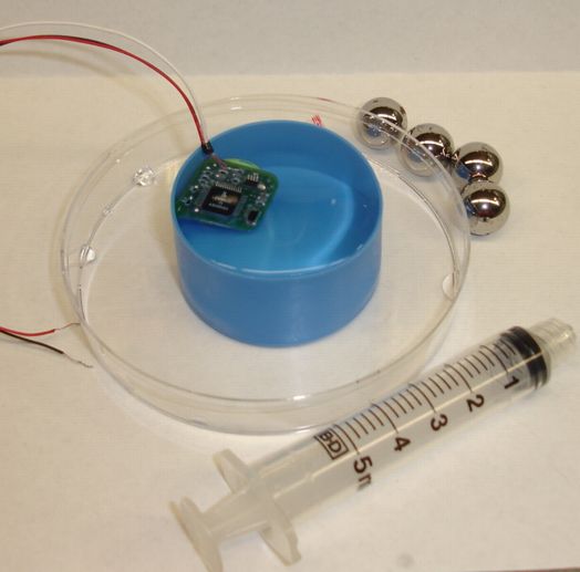
We fill the blue cup with water until the surface is flat and flush with the rim of the cup, as seen when looking across the water surface from the side. We place the object whose volume we wish to measure in the cup. Provided that the object's volume is less than 5 ml, the water does not spill out, but bulges upwards with surface tension, as shown in the figure. Now we remove water with a syringe until the surface is once again flat. The volume of water we removed is the volume of the object we placed in the cup.
We calibrated the measurement with four half-inch steel spheres. These each have volume 1.07 ml. Our measurement of the volume of two such spheres was on average 2.1 ml, with precision 0.1 ml.
| Object | Volume (ml) |
|---|---|
| 1 Half-Inch Sphere | 1.0 |
| 2 Half-Inch Spheres | 2.1 |
| 3 Half-Inch Spheres | 3.2 |
| A3013A, Silicone Coating, Process I | 2.0 |
| A3013B, Epoxy in Mold | 3.8 |
| A3013A, Epoxy and Silicone Coating, Process X | 2.4 |
| A3013A, Epoxy and Silicone Coating, Process A | 2.1 |
| A3013A, Epoxy and Silicone Coating, Process B | 2.4 |
| A3013A with Leads, Epoxy and Silicone Coating, Process B | 2.9 |
As you can see from the table, the volume of our final encapsulation, Process A, is 2.1 ml. The resulting transmitter is both water-proof and vacuum-resistant..
[15-FEB-10] Our Process B is more rugged, with helical steel wires and a curled antenna in a silicone tube. We measured the volume of nine of them together, with their leads, in a graduated cylinder. The total volume was 29 ml. We measured all ten transmitter volumes individually in the graduated cylinder without their leads. The minimum, average, and maximum volumes were 2.2 ml, 2.5 ml, and 2.6 ml respectively.
[21-JAN-10] For a picture of our first twelve A3013 circuits, see here. Two of them are in our epoxy mold. These later failed after we broke them out of the mold. All the circuits are hand-made.
We paint the serial number, version letter, and channel number of each transmitter on the bag in which we ship it to you. We do not mark the transmitters themselves. When the transmitter provides two channels, the number marked on the transmitter will always be even and correspond to channel X. Channel Y will be transmitted with an number one greater than X.
| Serial Number |
Channel Number |
Inactive Current (μA) |
Active Current (μA) |
Clock Divisors |
Low Frequency (ADC Counts) |
Comment |
|---|---|---|---|---|---|---|
| 001 | 1 | 19.3 | 83.5 | 21, 12 | 11 | Broken, Epoxy Encapsulation |
| 002 | 2 | 19.5 | 83.6 | 22, 13 | 10 | Noisy Signal, Epoxy Encapsulation, to ION |
| 003 | 10 | 18.8 | 80.4 | 22, 13 | 10 | Silicone Coating, to ION |
| 004 | 4 | 18.4 | 82.1 | 22, 13 | 11 | Silicone Coating, to ION |
| 005 | 5 | 19.0 | 80.0 | 22, 13 | 11 | Uncoated, Extension, to ION |
| 006 | 6 | 18.7 | 76.8 | 22, 13 | 8 | Unncoated, Extension, to ION |
| 007 | 7 | 20.6 | 75.6 | 22, 13 | 10 | Silicone Coating, 10% Missing Messages, to ION |
| 008 | 8 | 17.5 | 72.5 | 21, 12 | 11 | Silicone Coating, to ION |
| 009 | 9 | 20.5 | 75.5 | 22, 13 | 11 | Silicone Coating, to ION |
| 010 | 2/3 | 19.5 | 73.2 | 22, 13 | 9 | Silicone Coating, A3013D, to ION |
| 011 | 11 | 19.0 | 71.7 | 23, 13 | 10 | Silicone Coating, 10% Missing Messages, with OSI |
| 012 | 12 | 19.4 | 74.1 | 23, 13 | 11 | Broken, Uncoated, to ION |
| 013 | 4/5 | − | − | 23, 13 | 11 | Noisy, Epoxy Encapsulation, A3013B, with OSI |
The table above shows how the current consumption of our first twelve production-version A3013s varied from one circuit to the next. The consistency we see in the current consumption suggests that our assembly process is in no way damaging the logic chip. The variation in the DAC value required for a 915-MHz low-frequency shows variation between oscillator chips.
Two transmitters suffered from roughly 10% missing messages. These were numbers 007 and 011. In August 2007, we refurbished 011 and measured its RF output power spectrum with our new A3008B spectrometer. The RF spectrum covered 924±9 MHz. We placed a 4-kΩ resistor across R4, and so dropped the spectrum to 917±9 MHz. The missing message rate for 011 after this modification dropped to 0%. We conclude that improper initial calibration of the Low Frequency ADC Count caused the missing message rate in both these transmitters.
[17-FEB-09] Our machine-made A3013A-N circuits have slightly lower current consumption. The first 24 circuits we calibrated and tested had an average sleeping consumption of 22 μA and an average active consumption of 73 μm A.
[21-JAN-10] Here we present new measurements and observations made with the help of the A3013A.
As we report in SCT Encapsulation, stranded wires conduct water by capillary action, and so transport bodily fluids into the transmitter, disturb its analog inputs, and drain its battery. Solid wires appear to be immune to this capillary action because they do not have spaces inside the insulation along which water can creep.
We are happy to use teflon-insulated, solid, silver wires for our X inputs. But we wonder if the antenna will be efficient with such a thin wire. We set tried various types of wire for our transmitting antenna, and recorded the power received by our RF Spectrometer (A3008B) at a range of 30 cm for each antenna. The transmitting antenna was vertical in each case. The receiving antenna is a Loop Antenna (A3015L) You will find our results below.
| Insulation | Outer Diameter (mm) |
Wires | Conductor Diameter (mm) |
Peak Power (dBm) |
|---|---|---|---|---|
| red, teflon | 0.70 | solid, tinned, copper | 0.44 | −42 |
| white, teflon | 0.81 | seven strands, tinned, copper | 0.36 | −44 |
| green, PVC | 1.2 | solid, tinned, copper | 0.68 | −42 |
| white, PVC | 1.5 | seven strands, tinned, copper | 0.78 | −43 |
| none | none | solid, tinned, copper | 0.10 | −42 |
| none | none | solid, tinned, copper | 1.7 | −43 |
| clear, teflon | 0.28 | solid, silver | 0.20 | −43 |
| none | none | none | 0.00 | −71 |
It appears that the diameter of the conductor plays very little part in its efficiency as an antenna. We see no reason why we cannot use 0.2-mmm solid silver wire as our antenna, as well as our X inputs. Even 0.1-mm copper wire performed well as an antenna.
We first began to pay attention to the voltage on the antenna output when we studied damaged transmitters. According to the MAX2624 data sheet, our RF output is coupled through a capacitor on the chip. But we find that we cannot connect a loop antenna directly to the RF output and ground the other end. The MAX2624 stops working when you make a DC connection between OUT and 0V. In our damaged transmitters, OUT is connected to VBAT (see schematic). Among transmitters that have been operating for several weeks, roughly a third have OUT connected to VBAT. Freshly-made transmitters never have OUT connected VBAT.
We cannot make electrical contact with 0V when a transmitter is encapsulated, but we can get to VCOM (which is 1.80 V) at X−. We measured the voltage between OUT and VCOM in one of our encapsulated transmitters, and found it to be 0.95 V. This suggests OUT is connected to VBAT, and that VBAT is 2.65 V. When connect OUT and VCOM with 10 kΩ, the voltage between OUT and VCOM drops from 0.95 V to 0.2 V. We conclude that OUT is connected to VBAT with a DC resistance of order 40 kΩ. This connection was not present when we first turned the transmitter on. At some point, during weeks of operation, the MAX2624 suffered some kind of internal damage, and as a result, its OUT pin became connected to VBAT with a 40-kΩ reistance.
When we immerse a transmitter in water, it is possible for conduction to occur between the X− and antenna leads. If conduction occurs with impedance less than a 1 MΩ, we will find our battery life decreased. Future transmitters provide a discrete capacitor in series with the antenna, to make sure there is no DC current path between X− and either 0V or VBAT. But such a capacitor will not protect the transmitter from internal damage, as we showed in Damaged Transmitters.
We worked with two encapsulated transmitters that showed VBAT on the antenna. After working with both for a while, using different antenna lengths for an experiment described below, both transmitters stopped working. Several months later, we received three transmitters back from London. They all worked when we first turned them on, but their antenna wires were broken off. When we soldered new wires onto the transmitter contact pins, we connected the three pins together with a large solder ball to clean them. After this experience, two out of the three transmitters were broken.
[26-JAN-09] We received four A3013As encapsulated with Process X back from UCL. These transmitters had not been removed from their bags. We recalled them because we wanted to replace their solid steel wires with stranded wires. All four transmitters worked. Before removing the wires, we found that three transmitters had voltage VBAT on OUT. After replacing the wires, one of these three had failed. The other two worked well, except for the VBAT on OUT. The fourth transmitter functioned normally in all respects. We notice that the transmitters have a tendancy to turn on when we place them on our work bench, peel off silicone with steel tweezers, and solder the pins. We did not check these transmitters for VBAT on OUT after encapsulation.
We conclude that we are damaging some transmitters after encapsulation because they turn on while we are soldering their antenna leads in place. The soldering of the leads after encapsulation is a feature of Process X but not of the buried-wire Process A.
[13-FEB-09] We prepare a damaged transmitter, ID=8. We twist its analog leads together. We leave the tip of the antenna sticking out of its insulation. We covered the solder joints with heat shrink and dip them in silicone. We place the transmitter in water in such a way that the tips of the analog leads are out of the water, in air, and the tip of the antenna is immersed. We see a 1-mV 60-Hz sin wave on X. The battery in this transmitter was installed four months ago, so we expect four weeks of its nine-week operating life have been used up. We will now leave the transmitter in water and see if the presense of VBAT on OUT in water causes early discharge of the battery or failure of the RF power source.
We prepare another damaged transmitter, ID=9. We insulate the tip of the antenna with a blob of silicone, and we install extra-long stranded wires. We put this one in the water as well.
[18-FEB-09] The damaged transmitter without antenna insulation will not turn on with a magnet. In the previous few days, we noted that it's analog signal behaved erratically. Sometimes it would jump. Sometimes it would be insensitive. Sometimes it behaved normally. We banged it on the table a few times and it turned on. Now it's analog input is picking up 1 mV of mains hum. When we put it in water, the signal disappears, even though the tips of the analog leads and the antenna are out of the water. An hour later, the transmitter turns itself off. We bang it a dozen times on the table and it turns on again. Meanwhile, the other transmitter, with the insulated antenna, has been behaving perfectly.
The encapsulated transmitter shown here has its output leads soldered to pins. It is our first water-proof tranmsitter with output pins, and our first opportunity to vary antenna length in water and measure transmitted power. Once we are finished cutting back the antenna, we can replace it with a new wire.
We placed a transmitter in a 2-liter beaker of water by holding it by the body just below the water surface in the center of the body of water, with a straight antenna facing down. We placed the beaker 50 cm from a Loop Antenna (A3015L) and conneted the antenna to a Spectrometer (A3008B). We used our LWDAQ Spectrometer Tool to measure the power received by the antenna.
Our antenna is a 0.28-mm diameter teflon-insulated wire for our antenna. We started with a total antenna length of 125 mm, including the 4-mm connector pin, which protruded from the transmitter's ground plane, but not including the 5-mm trace from the RF power source, which runs on top of the ground plane. The graph below shows the variation in received power with antenna length, both with the antenna in the beaker and out of it.
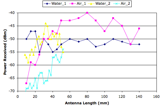
We measured the power transmitted in air by holding the antenna in the same orientation outside the beaker, at the same range from the antenna. In this first experiment, we damaged two transmitters. We did not turn off the transmitters when we cut back their antennas, so they may have been damaged by contact with our metal snips, as we describe above.
[23-OCT-08] We repeated the above experiment, this time with a epoxy-encapsulated transmitter with pins and a steel antenna wire. We turned off the transmitter while we cut short the antenna. We placed a 500-ml beaker of water 15 cm from our A3008C antenna. We stood the transmitter straight up in the water, resting upon the bottom. We used a straight antenna wire. We moved the beaker aside for the measurements in air. Peak power in water occurs at roughly 30 mm in both experiments. A 30-mm antenna transmits 20 dB more power out of our 500-ml beaker water than it does in air.
A 915-MHz quarter-wave antenna over a large ground plane will be 81 mm long in air and 9 mm long in water. Our antenna is more like an asymmetric dipole, with the battery forming one side and the wire forming the other. Its most efficient length in water is not 9 mm but 30 mm. A 50-mm antenna produces as much power in water as it does in air. Under the skin of a rat, we expect this antenna to perform better still, and so we choose 50 mm as the optimum length for our A3013 antennas.
Our work on omnidirectional antennas showed that a bent antenna for the transmitter, and a poorly-tuned loop antenna for the receiver, gives the most robust reception of transmitter messages. Each antenna has a direction in which it is least sensitive and least powerful. A straight antenna is insensitive in the direction of its length, and radiates very little power in that direction. Although the bent antenna does not transmit as much total power as a straight antenna, its minimum power transmission along its least efficient direction is ten times greater.
Once we introduced faraday enclosures into the transmitter system, reception became so robust that we thought we could save ourselves the trouble of putting a bend in our antennas. Our transmitters looked like this. But we soon found that reception from these straight antennas was less reliable. The plot below shows reception from three implanted transmitters. Transmitter No1 has a bent antenna. Transmitters No5 and No6 have straight antennas. Transmitter No1 and No6 are inside a faraday enclosure with a receiving antenna. Transmitter No5 is outside the enclosure with no receiving antenna. We receive no signal from No5.
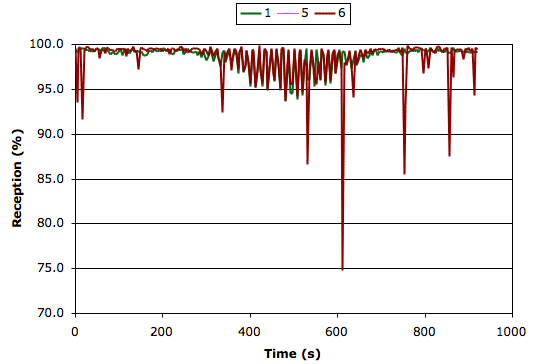
We see collision cycles in the reception, which are the result of No1 and No6 interfering with one another. But we also see drops in reception from No6 that are the result of the No6 antenna being in unfavorable orientations and positions. We see no such drops in reception from No1, with its bent antenna. We conclude that the bend in the antenna is well worth the trouble.
[21-JAN-10] Here we present the evolution of EEG recording using the A3013A. We begin with transmitters that fail because of problems with encapsulation and wires. We end with transmitters that provide pure EEG reception for their entire operating life. Reception from the transmitters varies from poor to good until we introduce faraday enclosures into the system, after which reception is excellent.
The first successful implant of a transmitter was in July 2007 by ION. The transmitter resided in a rat for three weeks, with X+ protruding down into its brain, and X− wrapped around a grounding screw. In the third week, ION provoked epileptic seizures in the animal by injecting kainate into the rat's blood. Previous implants in the animal laboratory had ended with the transmitter failing after several hours or days. While the implanted transmitters were working, however, signal reception was good, with no more than 50 messages being lost per second even during seizures.
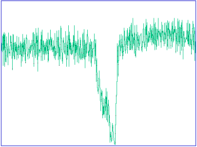
The figure below shows an example of one of the quieter moments during the recording, and one of the loudest. The rms amplitude of the quiet signal is around 50 μV, and of the loud signal is around 500 μV.
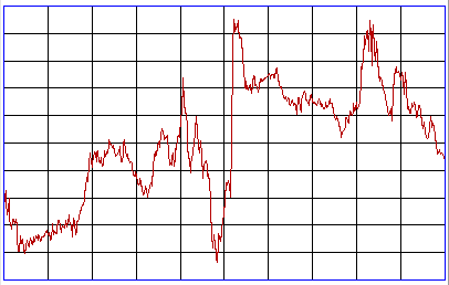
Of more interest to neurologists are the following traces, which we provide together with their fourier transform, as produced by the Neuroarchiver. According to Matthew Walker, "The first demonstrates high frequency fast activity at the beginning of the seizure and the second demonstrates repetitive spikes at 2-3 Hz with superimposed faster activity."
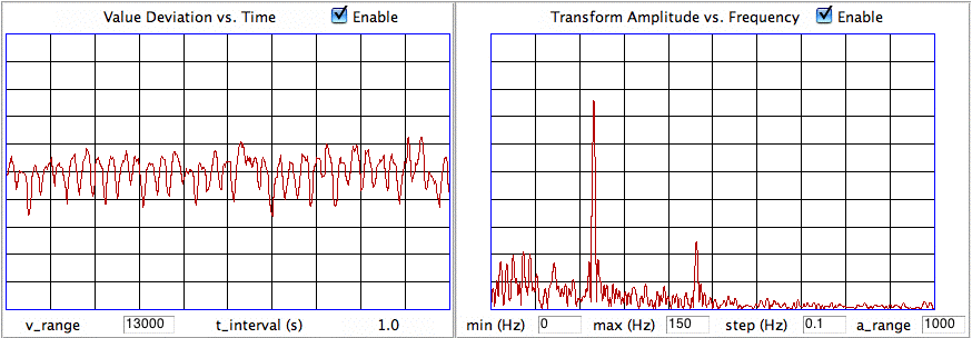
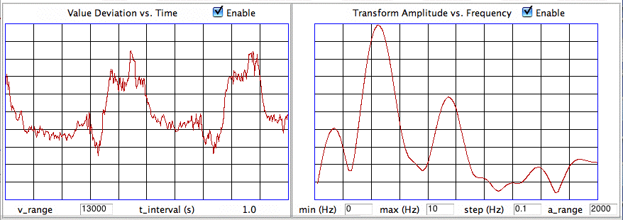
The fast oscillations show a sharp peak in the frequency spectrum at 35 Hz, with a sharp second harmonic at 70 Hz. But there is no third harmonic at 105 Hz, nor a fourth harmonic at 140 Hz. If either of these harmonics were present in the signal, we would see them with the A3013A's X input, because its bandwidth is 160 Hz, as shown here. After three weeks with the transmitter implanted, the rat died. For raw data recorded over five seconds from the recently-deceased brain, see here.
[20-FEB-08] Three transmitters implanted in rats in ION, London, provided robust transmission at range 50 cm. During 20 seconds of data from two moving rats simultaneously, we obtained 95% message reception 90% of the time, and 80% or greater reception the remaining 10% of the time. These transmitters failed after a day or two when their solid-conductor, copper and silver wires broke from repetetive stress.
[16-MAY-08] Pishan Chang of ION, London, implanted one transmitter with steel wires and epoxy encapsulation in a rat on 09-MAY-08. On 15-MAY-08 she began taking hourly data from the transmitter, recording its average X value and number of messages received in a one-second period. From the average X we estimate the transmitter battery voltage. From the number of messages received, we deduce the percentage of messages transmitted that were received correctly. We plot battery voltage and reception percentage below.
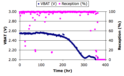
[20-MAY-08] At hour 120, we find that 95% of our samples show reception of 80% or greater, which is sufficient to support our 160-Hz bandwidth. Pishan believes the poor reception 5% of the time is due to unfavorable orientation of the animal.

[21-MAY-08] We receive the picture above from Pishan at ION. We suspect the metal lid of the cage is responsible for some poor reception orientations. With the rat standing in the far corner from the antenna, the reflection off the lid will be strong and opposite to the line-of-sight signal. For a close-up of the animal, see here. For a view of the ION animal laboratory see here. The laboratory appears to be free of metal obstructions near the cage, and is therefore well-suited for robust reception.
[23-MAY-08] The battery voltage has begun a gradual decline, which we have already observed when we are roughly half-way through the battery's operating life. Our hope is that the battery will last another four weeks, or 700 hours. We now have almost 200 hourly data points, of which only 9 exhibit less than 80% message reception.
[27-MAY-08] Battery voltage has dropped to 2.1 V. The transmitter will fail soon. We are at first disappointed, but then we add up the total current consumption from this particular battery as follows. First, there was a 100-hr burn-in in January with the transmitter in salt-water. Then the transmitter ran for 100 hours at ION while its wires broke off. It ran for 100 hours before ION began taking data in this most recent experiment, and 300 hours during data taking. That's 600 hours of active life total, for 80 μA × 600 hr = 48 mA-hr. The battery was fresh on 27-DEC-07, so it has provided quiescent current for 3000 hours, which consumed 20 μA × 3000 hr = 60 mA-hr. That's a total of 108 mA-hr. The battery capacity is 120 mA-hr. Perhaps we have forgotten another 100 hrs of active life somewhere along the way.
[29-MAY-08] Transmitter is still running. Battery voltage is 2.05 V.
[02-JUN-08] Transmitter failed at 2.00 V after a total of 675 hours of operation and 3000 hours sitting on the shelf. The wires survived 475 hours in the animal without failure. The battery voltage appears to rise after it descends to 2.0 V, and then decend again. This apparant rise in battery voltage may be real, or it may be a failure in our measurement of battery voltage, which is based upon the average value of the analog input. The ADC is not guaranteed to work below 2.7 V. We find it works well down to 2.3 V, but at 2.0 V, it may fail to convert properly, giving rise to an apparant increase in battery voltage when in fact the battery voltage is dropping.
[15-AUG-08] The rat containing the transmitter has doubled in size. ION removes the transmitter. Its analog leads have snapped at the animal's neck. ION implanted another transmitter in a live animal. The transmitter ran for two weeks, recording seizures with 95% message reception. After two weeks, the rat escaped from its cage and squeezed into a cupboard through a narrow gap. The transmitter reception afterwards was poor, and the recorded voltage jumped from one end of the dynamic range to the other.
[15-SEP-08] Received two transmitters from ION. The first is the one that resided for twelve weeks in a rat that doubled in size. The analog wires snapped half-way along their length. All three wires were broken at the base, but still held in place by their coating of silicone dispersion. The analog leads broke at the solder joints. The antenna broke 1 mm from the solder joint. We suspect that these leads broke because the rat doubled in length. Even the antenna would then be under stress because its loop would be held in place by fibrous tissue.
The second transmitter we received is from the rat that escaped its cage. Both its analog wires and the antenna are snapped off at the base. It appears that water penetrated under the silicone and smudged the ink on the ID label. The battery is run down to 30 mV. We know that these leads broke while the rat was loose from its cage. Reception was perfect before, and failing afterwards. We suspect that the strain put upon the transmitter by passage through a narrow gap with the rat's body pulled the wires off their joints.
[12-JAN-09] Pishan at ION implanted four transmitters in four separate rats on 08-JAN-09 and 09-JAN-09. Today she sent us 150 seconds worth of simultaneous recordings from all four transmitters in a single NDF file. Below is a graph of reception rate with time for all four transmitters.

We understand that the antenna is placed at the center of the four cages. There is a period of a few seconds when reception from Channel 4 drops below 50%, but otherwise reception is above 80% for all channels.
Pishan coiled the wires around a pencil and stretched them out into a spring spiral before she implanted the transmitters under the skin of the neck. Three days later, the input from Channel 3 appears to be disconnected. This means at least one wire has broken off Device 3. But its antenna is still intact, as are all twelve of the remaining leads.
[20-JAN-09] Twelve days after implanting, the reception from these four transmitters has degraded. Only one appears to have a functioning antenna. We assume that the antennas of devices 3, 4, and 9 have snapped off or broken in half. Furthermore, the EEG signals recorded from all four transmitters to not match our expectations. All four X inputs are disconnected. We have success with simultaneous transmission from four devices, but failure of the wires.
[11-FEB-09] Pishan reports that all wires on all four transmitters have broken at the solder joints.
[18-FEB-09] The previous plot shows no sign of a peak in the spectrum at 50-Hz. When we examine one second of data, which would be fifty cycles of the European mains hum, we see less than 15 μV. The plots below show eight seconds of data from an implanted transmitter, and we see less than 2 μV of mains hum.
The above data is consistent with every transmitter we implant. We see no significant pick-up of mains hum. Thermal noise in the band 48 Hz to 52 Hz is 1.5 μV. What we see is consistent with thermal noise.
[06-MAR-09] Two transmitters with 7 × 100 μm teflon-insulated antennas have been operating in two live animals since 10-FEB-09, and another two since 19-FEB-09. We report upon the status of the leads in SCL Trials. The receiving antenna is set up between four cages. When we visited ION on 27-FEB-09 we found that reception with the antenna at the common corner of the four cages was unreliable. Without the animals moving at all, we observed reception from two or more transmitters would cease almost entirely for a period of a minute at a time. With the antenna centered between the long sides of two cages, however, reception was always reliable for the transmitters in the two cages. Pishan has since confirmed our observations. It may be that a 900-MHz cordless phone in the building is disrupting our reception.
[31-MAR-09] Inadvertently record heart rate, as shown below.
[14-JUL-09] ION implants transmitter No11 with silicone-insulated helical steel leads, a 7×7 silicone-insulated antenna, and encapsulated by Process B. The animal is in a plastic cage with a metal wire roof. The plastic cage is inside one of our two-animal faraday enclosures. Reception is superb, at 99%. Analog signals look perfect.

[27-JUL-09] At ION, Pishan records EEG before and during a seizure using the Neuroarchiver. Each of the following images is a screen capture of the Neuroarchvier showing eight seconds of data on the left, with a full-scale range of 1.5 mV vertically and a fourier transform on the right, showing frequency content from 0 Hz to 100 Hz. The EEG before seizure is shown in Seizure_0.gif. The onset of seizure, where no outward signs of seizure can be observed, is shown in Seizure_1.gif. There follow three more images, which Pishan labeled with stage numbers we assume have some significance in the field of epilepsy: Seizure_2.gif, Seizure_4.gif, Seizure_5.gif.
[24-AUG-09] We obtain 250 s of data from two transmitters in a faraday enclosure in London. We plot the fraction of messages received during quarter-second intervals here. We see cyclic changes in message reception. Most of the time, reception from both transmitters is around 99%. But every twelve seconds or so, reception from both transmitters drops below 98%. In some cases, reception from No11 drops to zero. The cyclic variation is caused by collisions between the messages from both transmitters. As the transmitter clocks drift in and out of synchronization, the collision frequency comes and goes. The drops to zero are not caused by collisions. They are the result of signal loss independent of the second transmitter. We obtain a clearer demonstration of the collision sequence between two transmitters when we place two in a enclosure and do not move them, as you can see here. For a detailed discussion of collisions between A3013 transmitters, see the Collisions section of Subcutaneous Transmitters.
[28-AUG-09] Today we visited ION. Transmitter No11 has been operating for over six weeks in a live animal. Transmitter No4 has been operating for one week. Reception from both transmitters is superb and analog signals look perfect. ION and OSI agree that development of the A3013A is now complete. The system was ready for application in epilepsy studies.
[04-SEP-09] Record severe seizures in an epileptic rat at ION. Retrieve an exhausted transmitter from another animal. The exhausted transmitter spent seven weeks in the animal and appears to be unharmed by the experience.
[30-OCT-09] Two transmitters have been running implanted in a faraday enclosure for several weeks. We have seen no failures of transmitters other than by battery exhaustion. We observe that transmitters with straight antennas provide less robust reception than those with bent antennas, as we describe above. Pishan implants the transmitters by making three incisions: one on the animal's back, another at the neck, and one on the skull, as shown here. She places the transmitter under the skin at the back. She secures the transmitter by tying a thread around the groove between the battery and the circuit board and stitching this thread to some nearby animal tissue (we are not clear what tissue). She runs the leads to the incision at the neck with the help of some sort of tube, and then on to the head, where she secures one lead tip into a hole in the skull with the help of a screw, and holds the other lead on the skull surface with one or more other screws. She covers the screws with dental cement.
[30-NOV-09] Record seizures, as shown below.
[21-DEC-09] Reception has been poor with two faraday enclosures at ION for the past two months. With only one enclosure, the system works well. But today, the system is working well with four transmitters in two enclosures. For a graph of reception versus time during a 600-s recording, see here.
[21-JAN-10] Reception was perfect for five weeks, with the final transmitter nearing exhaustion today.
[06-JAN-25] We discontinued the A3013 in 2010, but it was our first successful subcutaneous transmitter. The A3013A-E provided robust and continuous signal monitoring for up to nine weeks when implanted in a live animal and operated within a faraday enclosure. The transmitter encapsulation was unaffected by vacuume and entirely water-proof. The transmitter was equipped with three subcutaneous leads that endured the repetetive movements of the animal without breaking. The silicone-coated antenna remained intact and isolated from the body fluid.
