The Demodulating Receiver (A3017) contains a 902−930 MHz 30-dB amplifier, a downshifer, a 60-dB 50-MHz limiting IF amplifier, a frequency discriminator, and an amplitude demodulator. The A301701A circuit board also includes, just for good measure, more copies of the A3016SO SAW Oscillator and the A3008C Spectrometer. If you can't understand our terminology (RF, IF, LO, dB, dBm, etc), please consult our Terminology page.
S3017_1: RF Amplifier, Downshifter, IF Amplifier, and Discriminator. Changes from A3017A to A3017B are noted.
S3017_2: Demodulator and Power Supplies.
BOM: Bill of Materials.
[01-FEB-07] Below you see the A3017A RF Amplifier layout next to its predecessor, the A3016DR RF Amplifier. The former amplifier worked well: 27-dB of stable gain from the RF input to the IF output after the mixer and IF low-pass filter. Consult the A3016DR manual for measurements of the RF passband. The new, unmodified amplifier, as shown below, oscillates.
It's not the missing capacitors around L201 that stopped oscillation in the previous amplifier. As we describe here, we replaced these capacitors with solder lumps in the previous amplifier, and it was stable.
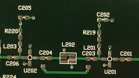
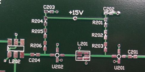
We applied copper tape, cut tracks, changed resistors, and soldered wire links. So far as we can tell, the problem is the loop closed by our +15 V power tracks. In the previous layout, +15 V came up through the ground plane in two separate places for the two amplifier stages. In this layout, +15 V comes up through the same ground plane penetration. The figure below shows our solution for the A3017A, which is the version we use in the A3018A and A3018B).
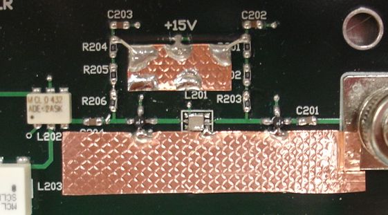
[05-AUG-10] We built three more A3017As using a new batch of ERA-3SM amplifiers. These have slightly different markings. Despite rectangles of copper tape as shown above, the RF Amplifiers of all three units were unstable. At first they passed our tests because they were stable when the input was connected to a 50-Ω terminator or attenuator, as is the case when we test the Demodulator and when we test reception with an attenuator in series with the antenna cable. But when the signal is weak at the antenna, and we connect the cable and antenna directly, the RF Amplifier tended to oscillate, especially when we put the lid on the Data Receiver (A3018B) that included the A3017A. We measured the thermal noise at point IFL in the circuit for the new A3017A and an older A3017A. The newer A3017A thermal noise was 3 dB larger, which suggests that the newer amplifiers have slightly higher gain, and this higher gain is the source of our intermittent oscillations.
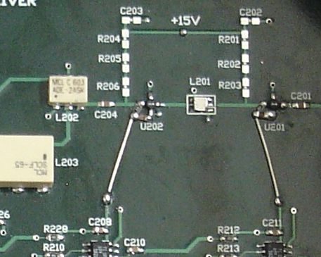
The A3017B uses the modification shown below to stop oscillations in the RF Amplifier. We power U201 and U202 with +5 V instead of +15 V, and use 50 Ω resistors to deliver the power. This modification reduces the gain of both amplifiers and removes the +15 V power supply loop.
The A3017B is stable with and without the lid, with and without the lid screwed in place, and with and without a 50-Ω terminator on its RF input. The RF to IF gain is around 23 dB, which is 6 dB less than that of the A3017A. The amplifiers provide 20 dB gain with 350-Ω bias resistors, but only 17 dB with 50-Ω resistors. We attempt to compensate for the 6 dB loss by increasing the gain of the IF Amplifier, but we doubt these efforts were successful (see below).
[01-FEB-07] The printed circuit board traces that connect the amplifiers are 30 mils wide (0.75 mm). The thickness of the circuit board is 62 mils (1.6 mm). The circuit board contains four layers of copper traces. The top layer is the one we see in the figure, with the 30-mil traces. The second layer is a continuous plain connected to 0 V, which we call the ground plain. A 30-mil trace 20 mils above a ground plane makes a 50-Ω transmission line. We want the traces to look like 50-Ω transmission lines so that they do not reflect RF power (see Terminology). But we subsequently discovered that the ground plain was only 10 mils below the top layer. The correct width for a 50-Ω trace 10 mils above a ground plain is 15 mils. According to this calculator, our 30-mil traces 10 mils above a ground plane, separated by FR-4 fiberglass, act like 30-Ω transmission lines. These 30-Ω traces will reflect 10% of the power delivered by a 50-Ω source, and another 10% will reflect back into the 30-Ω trace where it ends in a 50-Ω load. So each 30-Ω traces introduces a loss of roughly 20%, or 2 dB. This 2 dB is small compared to our gain of 20 dB at each stage. Although our traces are twice as wide as they should be, we don't expect any dramatic drop in performance as a result.
We connected the A3017A RF input to the output of one of our Modulating Transmitters (A3014MT). The A3014MT was tuned to roughly 910 MHz. Its output is −4 dBm, and we passed it through 36 dB of attenuation, so the power deliverd to the RF input was −40 dBm. For LO we used our 864-MHz A3014SO, with its +9 dBm output. The A3017A's IF output was −14 dBm, so its RF to IF gain is 26 dB. According the manufacturer's data sheets, we can expect 20 dB of gain from each amplifier, 3 dB of loss in the SAW filter, 7 dB loss in the mixer, and 1 dB loss in the IF low-pass filter. Our expected gain is 29 dB.
We replaced the A3017A with our A3016DR. Its IF output with the same input was −12 dBm, for an RF to IF gain of 28 dB, only 1 dB lower than our expected gain. We switched the amplifiers, and used high-frequency capacitors insted of general purpose, but something about the A3017A layout causes a 2-dB loss of gain with respect to the A3016DR.
[15-OCT-08] We built two more A3017s with serial numbers P0194 and P0193. We found that U201 and U202 were failing in one of the new receivers after running for a few days. We changed R203 and R206 to 150 Ω. Now the amplifier quiescent current is 35 mA instead of 40 mA. We also found that water stuck under the SAW filter could reduce the gain by 6 dB. With the new resistors we obtain a −7 dBm output for a −36 dBm input (−4 dBm from the A2014MT, −30 dB attenuator, and −2 dB in a 36" cable). The total gain of the RF amplifier is now 29 dB. The IF power of receiver Q0127 with the same input was −10 dBm. We replaced U201, U202, R203, and R206 in receiver Q0127 and cleaned the circuit board. The IF power rose to −7 dBm. Receiver Q0127 failed in London: after running for a while, it would stop receiving. We suspect that long-term damage to U201 and U202 caused by the 40-mA quiescent current are to blame. Receiver Q0126, which has been running for two years in Boston, now shows a gain of +29 dB, without the modifications. We changed R203 and R204 and the gain remained unchanged.
With −4 dBm on the RF input, the IF output of the A3017A saturates at −2 dBm, which suggests U202 is producing around +10 dBm.
The figure below shows the IF output with RF input frequency for a −34 dB supplied by one of our Modulating Transmitters (A3014MT). The pass-band is defined by both the SAW filter (L201, a B3588) and the IF low-pass filter (L203, an SCLF-65) acting together. For a picture of the frequency response without the SAW filter, see here. (The linked image shows the response of the A3016DR without the SAW filter, and the A3016DR is almost identical to the A3017A). The cut-off at the low end of the passband is due to the SAW filter. The variations in response within the passband are also due to the SAW filter.

If we define the signal pass-band as lying betwen two −3 dB frequencies, then we see that the A3017A pass-band extends from 900 MHz to 930 MHz, which encloses the 902−928 MHz ISM band very nicely.
But we can also define the interference acceptance-band as lying between two −20 dB power frequencies. Mobile phone interference in the UK, for example, is ten times more powerful than our transmitter signals in the 930−950 MHz band (see here). If our rejection is only 20 dB in this band, our transmitter power will be only 10 dB greater than the interference, even with the antennas oriented favorably. The −20 dB pass-band of our RF amplifier is not easy to see in the figure above, because −20 dB is a 90% drop in amplitude. But we can measure the −20 dB pass-band with the help of different attenuators, and we find it to be 890−940 MHz. Without the IF low-pass filter, the −20 dB pass-band extends up to 950 MHz, and perhaps even as hight as 960 MHz. The IF low-pass filter is essential for removing 940−950 MHz interference from mobile phones in the UK. Our earlier Demodulating Receiver (A3005C) did not have this same low-pass filter, and was therefore vulnerable to interference in the UK, while performing well in the US.
The A3017A schematic specifies the B3588 SAW filter. Its pass-band is nominally 915±13 MHz. We tried the AFS915S3 instead. Its pass-band is nominally 915±4 MHz. Below are the RF frequencies responses for both filters, obtained in the same way as we did here, and using the same apparatus we describe below.

The AFS915S3 pass band is around 30 MHz, far wider than we suspected after reading the data sheet. The insertion loss of the AFS915S3 appears to be at least 3 dB higher than that of the B3588.
[06-AUG-10] We add the three OPA699 limiting op-amps that make up the A3017A's IF amplifier. They amplify the IF signal from the IF filter (L203 in the schematic) and produce the amplitude-limited IFL signal for the demodulator. In the A3017A, the IF Amplifier provides nominal gain of 62 dB (11×11×11 in voltage gain). In the A3017B, the IF Amplifier provides nominal gain 68 dB (21×11×11 in voltage gain). The output amplitude limited to ±700 mV. With no input, the output of the IF amplifier is white noise of amplitude 500 mV p-p. When we applied −64 dBm of 910-MHz to our RF input, the IFL signal you can see in the schematic saturated cleanly. When we applied −82 dBm, the IFL output was dominated by our 46-MHz IF signal, but noise was clearly visible.
[16-MAY-13] The OPA699 limiting amplifier has gain-bandwidth product 1000 MHz. Its typical bandwidth at gain ×11 is 91 MHz. The nominal gain of the first IF amplifier in the A3017B is ×21, for which the typical bandwidth will be 48 MHz. Thus we expect our IF amplifier to produce less gain at above 48 MHz. When the signal is weak, we expect to see failure of demodulation at the higher end of the IF spectrum before the lower end, like this.
The noise in our receiver is the thermal and amplifier noise at the antenna input. The interference is RF power in the receiver's pass-band arriving at the antenna from transmitters other than those the receiver is intended to receive.
We concern ourselves with noise and interference only at the antenna input. At all other points in the receiver, our signal is at least ten times more powerful. Noise and interference at the antenna input has at least ten times the effect as it does anywhere else.
The antenna input connects through a decoupling capacitor to the input of amplifier U201, which is a ERA-3SM. The capacitor generates no noise. But the 50-Ω input impedance of the amplifier generates thermal noise. Thermal noise is electronic noise that arises from the random, thermal movement of electrons. A circuit with bandwidth B suffers from noise power 4kTB, where k is the Boltzmann Constant with value 1.38×10⁻²³ J/K, and T is absolute temperature. Our pass-band is roughly 900-930 MHz, which is a bandwidth of 30 MHz. This gives us a thermal noise power of around 0.5 pW at the input of our RF amplifier. The ERA-3SM noise figure is 2.6 dB, which means that the effective noise power at its input is 2.6 dB higher (twice as great) as the thermal noise. Our effective RF input noise should be around 1 pW, or −90 dBm.
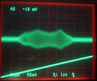
We disconnected the antenna and terminated the RF input with 50 Ω. We measured the rms amplitude of the signal at the output of U204 (see schematic). The total gain from the RF input to the output of U204 is 71 dB (29 dB in RF ampligier plus 42 dB in two stages of IF amplifier). The signal on the output of U204 has the appearance of white noise. We do our best to estimate its amplitude by triggering on zero-crossings and looking at 1 μs of output trace. The root mean square amplitude appears to be 20 mV, which corresponds to −86 dBm of input noise. Our expected input noise was −90 dBm.
We connected the antenna in our basement laboratory. The output of U204 is not random, but has peak-to-peak amplitude that varies from 400 mV to 1000 mV. The average amplitude is around 600 mV p-p, which corresponds to −68 dBm.
Our antenna noise power is −86 dBm and ambient interference is −68 dBm, which is 18 dB more powerful than the noise. Our sensitivity to transmissions is limited by interference. This means that if we put our antenna in series with a 12-dB attenuator, we should see very little loss in performance, because the attenuator attenuates both the interference and our signal. Certainly, a cable with attenuation 2 dB, like a 240-cm RG-58C/U cable we use with the A3015A will not degrade our sensitivity to transmissions.
We tested the A3017A in our OSI office, which is on the second floor of a large brick building on Main Street, Waltham. There are seven or eight 2.4 GHz wireless networks overlapping the office, and offices upstairs and on either side. Downstairs is a grocer. We saw no bad messages from interference. The amplitude at the output of U204 was a repeating 100-mV rms 50 MHz waveform, with bursts of 150 mV rms amplitude several times a second. If we take the bursts as our interference power, we arrive at −70 dBm, which is less than we observe in our basement laboratory.
We added the remaining parts to our A3017A, which completed the Discriminator and Demodulator. We applied a sweeping TUNE input to our Modulating Transmitter (A3014MT), and looked at the demodulator output versus frequency for various values of attenuation in the RF supply cable. We performed our measurements with the circuits on a wooden table, with no enclosure, as we detail below, we obtained much bette results when we eclosed them in a metal box

With a bare A3017A circuit board, the sweep worked only down to −64 dBm. We touched the SAW filter in the RF amplifier, and the sweep was effective down to −72 dBm. We wrapped foil around the entire A3017A, and the sweep was again effective down to −72 dBm. When we combined the A3017A with other circuits in a metal enclosure to make the Data Receiver (A3018A), the sweep was effective down to −76 dBm. There was no trace of the sweep when we disconnected the cable carrying the sweep RF power.
In theory, our sweep input is competing with the thermal noise at our antenna input. Our thermal noise power is −86 dBm (see above). Our sweep is effective down to −76 dBm, or 10 dB above the noise power. Compare this to our observed failure of message reception when the message power is less than 12 dB above the interference power.
In our original design of the Demodulator, the value of resistor R222 was 50 Ω. But we later changed R222 to 0 Ω. Nevertheless, we made the mistake of loading 50 Ω in some units. This 50-Ω resistor interacts with the discriminator in the A3007 to which the Demodulator output connects in the A3018. We show how the resistor affects reception here.
The A3017B, which uses +5V to power the RF Amplifier, is sensitive down to −72 dBm when the lid is secured, while the A3017A is sensitive to −76 dBm. If we place an Antenna Combiner (A3021B) between the power source and the A3017B, the A3021B adds 11 dB of gain and the A3017B is sensitive to signals down to −81 dBm.
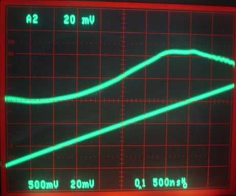
[FEB-07] We disconnected our source of RF power and inserted an 80-mm quarter-wave antenna into its RF output socket. We connected an A3015A loop antenna to the RF input of our A3017A via a 2.4-m (96") RG58 coaxial cable. We obtained the following trace.
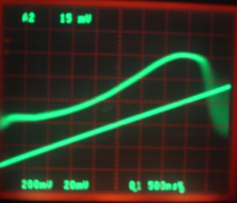

According to our antenna measurements, we expect a minimum 32 dB loss as our RF signal travels through a quarter-wave antenna, across 1 m, to a loop antenna and through a 240-cm cable. We expect a maximum loss 17 dB greater, or 49 dB. Across 2 m, we expect a mininum loss of 38 dB, and a maximum loss of 55 dB. Given that our RF source was −4 dBm, we expect our RF power at the antenna input to be between −59 dBm and −42 dBm. But our interference power, after passing through the 1-dB loss of the antenna cable, is −69 dBm. Our signal power is at most 27 dB greater than the interference, at least 10 dB greater, and almost everywhere it is 12 dB greater. This is what we observe: when we hold a transmitter at 2 m, we get reliable reception in almost every orientatioin.
With both antennas in favorable directions at 2 m, we should get 27 dB more signal than interference. Ignoring reflections, at 6 m we would get 12 dBm more than interference. So we expect our transmitters to work up to 6 m in the absense of reflections. In fact, we find that they work at up to 14 m in our lab.
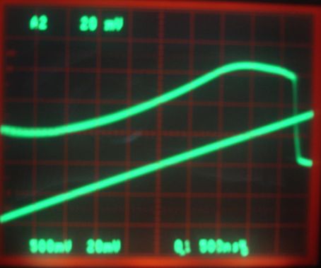
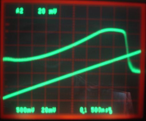
When we interposed our body between the two quarter-wave and loop antennas, we observed occasional sharp holes in the sweep respons. These are reception dead-spots, caused by destructive interference of the RF signal at the receiving antenna (see here and here). With a quarter-wave and dipole antenna, we were able to orient the two at range 2 m to obtain a reception dead spot without the use of our body. This allowed us to take a photograph of the dead spot as it appears in the response of antenna-to-antenna transmission power versus frequency. You can see clearly the hole caused by destructive interference at the receiving antenna.
To record messages from a transmitter, we must to connect the A3017 to a Data Recorder (A3007). We present the results of our work with these two circuits combined in our Subcutaneous Transmitter report.
[06-AUG-10] We compared the A3017A and A3017B radio reception by placing an A3013A in the corner of a faraday enclosure with an antenna at the enclosure center. We connected the antenna signal to the RF input via a 2.4-m coaxial cable and a 40-dB attenuator. Reception with an A3017A, working as part of an A3018B, was 97% with the lid on or off. Reception with one A3017B, working as part of an A3018C, was 94% with the lid on or off. Reception with a second A3017B was 98% with the lid on and off.
The A3017A suffered from oscillations in its RF amplifier, and in its early days from damage to the RF amplifier by over-heating. But the A3017B RF amplifier has proved stable and robust.
[20-JUN-11] We receive back from Louise Upton of Oxford University P0230, an A3017B installed in an A3018C data receiver. We found U206, a THS4082 dual op-amp, had a bad joint on pin 8, the +15V pin, although contact existed at the time we tested. The op-amp, however, could not drive a 50-Ω load. We replaced U206 and the circuit works fine. This circuit had been put through a gas sterilization. One possible cause of the failure was that the gas and heat opened the bad joint so that power was, for a brief time, applied to only −15 V, damaging the op-amp. We have had trouble with these op-amps being fragile in the past. Another possibility is that the LWDAQ power cable was improperly plugged in at some point, so that only -15 V or +15 V power was delivered, thus damaging the op-amp. We see no sign of damage to the A3018C's LWDAQ socket. We plugged and uplugged the LWDAQ cable twenty times and observed no damage.
[28-DEC-12] We find that P0193, which has been operating in our laboratory for the past couple of years continuously with no problems, now fails to receive signals from fourteen new transmitters. We re-calibrate our A3014MT modulating transmitters using our 910 MHz and 868 MHz reference oscillators and test the input response of P0193 to a −77 dBm sweep from 890 MHz to 950 MHz. The response looks okay, but we still find that P0231 and P0232, which we have on hand, have perfect reception from our fourteen transmitter, while P0193 misses half the messages. We re-calibrate our two A3008C spectrometers and confirm that the center frequency of the transmitter lies in the range 914-918 MHz. We notice that P0193 has trouble powering up. It brings down the ±15-V power supplies. It is U206 over-heating. We replace the THS4082 with an LM6172M dual op-amp. We suspect that the THS4082 was destroyed by asymmetric power in the past, as with the P0230 receiver discussed above. With the new op-amp in place, reception is perfect.
[11-JAN-13] We ship A3018 number P0231 to ION. Before we do, we replace U206 with an LM6172M.
[11-FEB-13] We have A3018C number Q0128 back from ION. It does not receive transmitter signals. We replace U206 with LM6172 and it works for a while, then stops receiving. We discover a solder lump on resting upon U207-5 and U207-4. We clean and now get good reception.
[07-AUG-13] We have A3018C number P0232 back from ION. It does not receive transmitter signals. This receiver was working fine at ION until they moved it to a new location and plugged it in. The THS4082 in U206 is blown. We replace U206 with LM6172. Now it works fine. We plug and unplug power fifty times. It still works. We decide to ship this unit to Edinburgh. We call this the A3017C.
[30-JAN-14] We have A3018C number P0230 back from Oxford University. We upgraded the A3007 firmware to version 7 and note that U206 is a THS4082. We replace it with LM6172M to make an A3017C.
[03-JUN-15] We have A3018D number Q0127 back from ION. It brings down the ±15 V power supplies. We remove U206, a THS4082 and replace with LM6172M. Now it works fine.
What limits reception now, in the faraday enclosure, is thermal noise. We see that reception is still robust from the far corner of a faraday enclosure, even if we reduce the received power by 40 dB, which is a factor of 10,000. Even if we allow for 10 dB loss in an animal body, 10 dB loss for poor antenna orientation, and 10 dB loss due to destructive interference, we still have 10 dB more signal than we need for robust reception.