
Figure: Antenna Combiner A3021B.
The Antenna Combiner (A3021) is an active combiner for four 50-Ω coaxial antenna connections. The output is a combination of the four inputs with net gain of roughly +11 dB. The A3021 is intended for use with four Loop Antennas (A3015B), each of which is placed in a separate faraday enclosure and receiving signals from subcutaneous transmitters.
The A3021 needs no terminators on its unused inputs. The circuit is unconditionally stable and isolates itself from local interference so effectively that it needs no shielding around the circuit board.
We supply +5V power to the A3021 through a shielded LWDAQ Cable. Current consumption is 140 mA. We connect the other end of the cable to a LWDAQ Driver. The only purpose of the LWDAQ Cable is to provide +5V power. No communication occurs between the A3021 and the LWDAQ Driver.
The A3021B is designed for use with the Data Receiver (A3018). The A3018 is a LWDAQ Device, and so its presence assures us of a LWDAQ Driver into which we can plug the A3021.

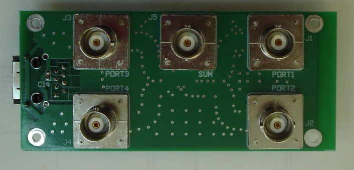
The A3021 amplifies its four inputs, combines them, and passes the sum through an attenuator on its way to the output connector. The input ports are P1 through P4 on the schematic, and PORT1 through PORT4 on the circuit board. The output port is S on the schematic and SUM on the circuit board.

The amplifiers provide gain to offset the loss introduced by the combiner. The combiner performs better when connected to a 50-Ω signal source, and the amplifiers always provide such a source, regardless of whether or not their own inputs are well-terminated. Furthermore, by amplifying the antenna signal before it passes through the combiner, we make sure the signal is as large as possible compared to our amplifier's thermal noise. The combiner attenuates the signal by almost 7 dB, so by placing the amplifier first, we improve our signal to noise ratio by 7 dB.
The attenuator at the output of the combiner provides a well-behaved impedance for the antenna combiner and for the cable, so that the signal propagation to the A3018 amplifier input will be involve no reflections. With a 4-dB attenuator on the combiner, the total gain from the input to the output of the combiner is around 11 dB.
S3021_1.gif: Active antenna combiner circuit diagram.
A301501B.zip: PCB Gerber Files. Six A301501B printed circuit boards plus an A3021A antenna combiner circuit.
A302101B.zip: PCB Gerber Files. Six A301501C printed circuit boards plus an A3021B antenna combiner circuit.
PPL Enclosure: Drawing of the hand-sized plastic enclosure in which we mount the Antenna Combiner.
[05-JAN-11] We tested the gain of our first A3021B with the help of a frequency sweep provided by one of our Modulating Transmitters (A3014MT). We sweep the frequency of the A3014MT with a triangle wave, as we describe here. We connect the A3014MT output through 1-m RG-58C/U cable to the RF (radio-frequency) input of a ZAD11 mixer. We obtain the LO (local-oscillator) input from an A3018C. We measure the IF (intermediate-frequency) amplitude with our oscilloscope for RF of 900 MHz and obtain the following table.
| Condition | Amplitude (mV p-p) | Power (dBm) |
|---|---|---|
| Reference | 150 | −12.5 |
| Add 20dB attenuator on A3014MT | 15 | −32.5 |
| Insert A3021B, P1 to S followed by 1-m Cable | 54 | −21.4 |
| Switch to P2 | 50 | −22.0 |
| Switch to P3 | 50 | −22.0 |
| Switch to P4 | 52 | −21.7 |
| Switch to P1, terminate P2 with 50 Ω | 53 | −21.5 |
| Terminate P3 | 52 | −21.7 |
| Terminate P4 | 50 | −22.0 |
| Remove terminators, palm pressed on circuit | 30 | −26.5 |
We cannot put the A3021B into oscillations with our hands, with microwave absorbent foam, with terminators, with unterminated cables, or by re-arrangements of cables. The circuit is unconditionally stable. Even when we put our palm on the entire microwave circuit, all that happens is the gain drops by 5 dB.
The gain of P1 drops from 11.1 dB to 10.5 dB when we add terminators to the other three inputs. The gain of the other channels is up to 0.6 dB less than for P1. With terminators on all unused channels, the minimum gain of the combiner is 10 dB. The amplifiers provide at least 21.3 dB at 900 MHz. The ERA-3SM data sheet gives a typical gain of 21 dB at 1 GHz.
We applied our A3014MT sweep through a 1-m cable to the A3021B, then a 1-m cable to our A3018C. We look at the demodulated D signal in the same way we did here. We added a 70 dB attenuator to the A3014MT output and obtained the following oscilloscope trace.

Another 6 dB of attenuation takes the A3018C a little past its minimum input power.

When used with the antenna combiner, the A3018C is sensitive to antenna signals as weak as −81 dBm. The combiner raises the A3018C's performance to that of the original A3018A, which we describe elsewhere, and does so for four antennas simultaneously with or without terminators on unused inputs.
We connected an FE2A enclosure containing an A3015B antenna to our A3018C with a 2.4-m cable. Inside the enclosure we have a transmitter near the wall. We inserted various attenuators at the end of the 2.4-m cable and measured average reception over 10 s. We inserted the A3021B between the A3018C and the cable, and performed the same experiment, with the attenuators at the P1 input. The graph below shows our results.

We see that the A3021B increases the sensitivity of the A3018C by 6 dB before reception drops below 80%.
We moved a transmitter around at random in our FE2A and measured average reception over one minute with and without the A3021B. We obtained 98.0% reception without the A3021B and 99.3% with the A3021B.
[10-JAN-11] We left the Neuroarchiver recording for a hundred hours. For a plot of hourly-average reception see here. For more details see here.
[27-JAN-11] We receive two hours of characteristics from Joost at ION. Reception from twelve transmitters in four faraday enclosures with the A3021B is superb, as we report here. Reception is near the theoretical maximum we can obtain with twelve colliding transmitters.
[01-FEB-11] We receive more characteristics from Joost at ION. The plot below shows reception in 4-s intervals during an hour of recording from twelve transmitters in four faraday enclosures. Transmitter No9 is implanted. The others are distributed around the corners of the enclosures.

Robustness for No9 is 97% and for all others is between 95% and 99.9%. Average reception for No9 is 89% and for all others is between 92% and 94%. Joost replaced the A3021B with a passive AC4A combiner and obtain this graph. Robustness for No9 drops to 85% and for all others is between 94% and 99.9%. Average reception for No9 is 83% and for all others is between 91% and 94%. The drop in robustness for No9 is striking. We see it as loss of signal for minutes at a time in the second graph. The A3021B appears to stop these minute-long losses.
[03-APR-11] We receive 15 hours of data recorded on 13-FEB-11 by Joost at ION with A3021B and eight implanted transmitters.

More detailed analysis reveals hourly drops from one transmitter or another for ten or twenty seconds. The overall average reception is 95%, which is what we expect from collisions. The hourly drop-outs we believe are due to multi-path interference.
[17-DEC-10] The A3021A had no inductors L1..L4, nor the blocking inductor L6. The layout carries the amplified antenna signals along 30-mil tracks over a ground plane. The characteristic impedance of such a trace is around 100 Ω (see this calculator). We connect power to the A3021A with a shielded LWDAQ Cable. We connect its output to our Demodulating Receiver (A3017B). We look at the IFL signal shown here. We see a large and sustained signal. Further observations confirm that the A3012A oscillates.

We can suppress the oscillations by touching it in just the right way, but not permanently. We apply a frequency sweep to one of the antenna inputs using our A3014MT. With the help of attenuators and the signals in the demodulating receiver, we determine that when it is not oscillating, the A3021A delivers a total gain of +6 dB. We expect −4 dB from the attenuator, −7 dB from the combiner, and we expect +17 dB from an ERA-3SM biased by 50-Ω, for a total of +6 dB of gain, which matches our observation.
With a −73 dBm sweep, we can just see the signal at ILF without the antenna combiner. We expect a stronger signal with the antenna combiner added. When we stop large oscillations, we see signs of a stronger sweep, but it is swamped by other noise or signs of smaller oscillations. The circuit is impractical and ineffective.
We read up on microwave circuit board layout, and consider the fact that the ERA-3SM provides plenty of gain right up to 10 GHz. We resolve to lay out our printed circuit board so that it will behave well at 10 GHz. The A3021B adds L1..L4 and L6, as well as C15. We provide 50-Ω transmission lines for the amplified signals in the form of coplanar wave-guides with ground. We can run curving signal tracks with a 7-mil (180-μm) gap between them and the coplanar ground traces, which are the 62-mil below the top copper. The board itself has only two layers. With the help of this calculator, we choose a wave-guide trace width of 1.25 mm (50 mils). We eliminate sharp corners on the signal path, and replace them with 3.75-mm (150-mil) radius bends. We fill all unused board area with ground planes, and join the top and bottom ground planes every few millimeters.

[05-JAN-11] We assemble the first A3021B, using a 4-dB attenuator for R5 (a LAT-4). The circuit performs well. It is stable regardless of termination or handling or cable arrangement. The amplifiers provide +22 dB of gain, which is more than we have ever observed from the ERA-3SM at 1 GHz. The circuit is stable with inductors in the gain impedance of the amplifiers, while we observed instability with such inductors in all our previous efforts.
[13-JAN-11] We assemble another A3021B and find it works first time.
[14-JAN-11] We assemble another A3021B. This time we used 47-pF capacitors instead of 100-pF because we had run out of the latter. Performance was indistiguishable from our first A3021B.