[02-FEB-24] The Subcutaneous Transmitter (A3047) is an implantable telemetry sensor that provides amplification and filtering of up to four independent biopotentials as well as a body temperature. The A3047 operates with our Subcutaneous Transmitter system. The A3047A displaces 3.0 ml, weighs 6.0 g, and is equipped with up to nine flexible leads. We turn the A3047 on and off with a magnet.

The maximum number of leads loaded on the A3047 is nine. One of them is always GND, the low-impedance ground connection. The GND lead is always blue. The ground lead anchors the potential of the transmitter circuit to the animal body. We must attach the ground lead to some part of the subject animal, preferably a part that is electrically inactive. Each amplifier may use GND as its reference potential, or it may use its own high-impedance reference input. The amplifier inputs are Xn+ and Xn−, for n = 1, 2, 3, and 4. The amplifier subtracts the potential of Xn− from the potential of Xn+. If we leave any input X+ or Xn− disconnected, the disconnected input assumes the same potential as GND. An input uses GND as its reference if we connect one of Xn+ or Xn− to a point of interest and leave the other input disconnected. An inputs uses is own high-impedance reference potential by connecting both Xn+ and Xn− to a point of interest. For example, we could use an A3047 to record two channels of EEG, one channel of ECG and one channel of EGG in the following way. We connect X3+ and X4+ to two depth electrodes in the hippocampus. We connect GND to the cerabellum. We connect X2+ and X2− to locations near the heart. We connect X1+ and X1− to locations near the gut. We have left X3− and X3− disconnected, so that they assume the ground potential. Our transmitter has seven leads.

The A3047's thermometer is on the bottom side of the circuit board, as shown in the photograph above. It's absolute accuracy is ±1.0°C and its stability and precision are better than ±0.1°C. With a one-point calibration at 37°C, the absolute accuracy improves to ±0.1°C. We use a processor like this in the Neuroplayer to translate the A3047's sixteen-bit output into a temperature, after which we can subtract an offset to obtain a calibrated measurement.
All versions of the A3047 are covered by a one-year warranty against corrosion and manufacturing defect.
[02-FEB-24] The following core versions of the A3047 exist. We define new versions upon request. The full part number is of the form "A3047Vn-L", where capital letter V specifies the battery, number n specifies the sample rates of the four channels, capital letter G specifies the bandwidth and gain of each channel, capital letter L specifies the configuration of the leads. We use the table below to translate VnG codes into transmitter characteristics. The L code we present a separate Leads table. The operating life is the minimum time for which a newly-made transmitter will operate continuously. The shelf life is the time the transmitter can remain turned off in storage and still retain 90% of its operating life.
| Version | X1 | X2 | X3 | X4 | T | Battery Capacity (μA-dy) |
Vol- ume (ml) |
Dimensions (mm) |
Mass (g) |
Oper- ating Life (dy) |
Shelf Life (mo) |
|---|---|---|---|---|---|---|---|---|---|---|---|
| A3047A1A | Disabled | 0.16-80 Hz, 256 SPS, 54 mV, CH=0 |
0.0-40 Hz, 128 SPS, 27 mV, CH=1 |
0.0-160 Hz, 512 SPS, 54 mV, CH=2 |
128 SPS, CH=3 |
11000 (CR2330) |
3.2 | 24 × 24 × 8 | 6.7 | 72 | 36 |
| A3047A1B | Disabled | 2-80 Hz, 256 SPS, 54 mV, CH=0 |
0.0-40 Hz, 128 SPS, 108 mV, CH=1 |
0.0-160 Hz, 512 SPS, 108 mV, CH=2 |
128 SPS, CH=3 |
11000 (CR2330) |
3.2 | 24 × 24 × 8 | 6.7 | 72 | 36 |
For each analog input we specify the bandwidth, sample rate, input dynamic range in millivolts, and channel number offset. The channel number offset is the value we add to the base channel number of the device to obtain the channel number of the signal.
| Code | X1+ | X1− | X2+ | X2− | X3+ | X3− | X4+ | X4− | Ground | Antenna |
|---|---|---|---|---|---|---|---|---|---|---|
| A | None | None | Yellow 100 mm B-Lead A-Coil |
Green 100 mm B-Lead A-Coil |
Orange 100 mm B-Lead A-Coil |
Purple 100 mm B-Lead A-Coil |
Red 200 mm B-Lead A-Coil |
None | Blue 200 mm B-Lead A-Coil |
Clear 50 mm A-Ant |
We define the lead names and provide links to photographs and drawings of the leads in the A3028 Manual's Leads section. We present the various antennas we have used for implants in the Antenna section. The best antenna for rat implantation is the 50-mm A-Antenna. We define the electrode names and provide links to photographs and drawings of the electrodes in the Catalog section of our Electrodes page.
The dynamic range of each signal is 0-65535 ADC counts (cnt). The zero-value of an input is the sample we obtain when we short the two inputs together. The nominal zero value for all inputs is 32768 counts. Offsets in the amplifiers cause variation in the zero-value sample of ±3000 counts from one channel to the next, and from one transmitter to the next. Once established, these offsets vary slowly with time and insignificantly with temperature.
For the thermometer, we specify the sample rate and the channel number offset. All thermometers provide the same accuracy and precision. We read out and digitize the temperature measurement with a fourteen-bit ADC. We add two zeros to the end of the fourteen-bit value to obtain a sixteen-bit value. The quantization step four our temperature measurement is four sixteen-bit ADC counts. The sensitivity of the digitized value to temperature is −5.25 mK/cnt. Because the minimum chnage in the sixteen-bit ADC value is four counts, the resolution of the thermometer is four times the magnitude of the sensitivity, or 0.021°C.
See below for details of current consumption and how to calculate battery life of new versions of the A3047. By default, we set the top of the frequency range at one third the sample rate. The A2047's low-pass filters provide 20 dB of attenuation at one half the sample rate. Frequencies above one half the sample rate will be distorted by sampling, and so compromise the fidelity of the recording. Because the EEG signal contains less and less power as frequency increases, this attenuation is sufficient to ensure that distortion is insignificant.
[26-FEB-24]The A3047 has ten pads for wires. One is A, the transmit antenna. The other nine are low-frequency analog inputs. We can see how they are arranged on the circuit board in the darwing below. We solder the end of each lead to one of the pads on the top side of the board, before loading the battery over the leads, and later burying their solder joints in the epoxy between the battery and the circuit.

The antenna lead, connected to A, is always present, and it is always clear-insulated, stranded stainless steel wire tied in a loop, joined to the base of the GND lead on the opposide side. The GND lead is always present, and must always be connected to the subject animal. It is the low-impedance ground potential for the amplifier inputs. Any amplifier may use GND as a reference by leaving one of its inputs open-circuit. Each amplifier is equipped with its own three-pole low-pass filter whose cut-off frequency we adjust by changing the values of three capacitors.
During our final quality control, we measure the frequency response of every A3047 amplifier. We apply a sinusoidal voltage to all inputs and plot the amplitude of the transmitted signal versus frequency. You will find a database of such plots here.

We connect a 0.2-Hz square wave of amplitude 50 mVpp with 10-MΩ source impedance. We expect a 25-mVpp signal on all three inputs. In the caption below we give the dynamic range of each input. Note that the X2 input relaxes after each square wave edge, while X3 and X4 do not, because their response extends to 0.0 Hz.

We apply a 100-mV triangle wave through 10 MΩ, so we expect 50-mV at the inputs. The triangle wave drives the X3 input into saturation on both sides of the dynamic range, and almost drives the other inputs to their limits as well. Note that the amplifiers are able to drive their outputs right to the positive and negative supply voltages. In X2 we see non-linearity in the ramp when emerging from saturation. This non-linearity arises only when the amplifier output is driven into saturation at the edges of the dynamic range.

Each of the amplifiers X1..X4 are equipped with non-inverting and inverting inputs so as to permit a differential voltage measurment. The low-impedance ground pad must be connected to some part of the subject body. If we make no connection to the inverting input of an amplifier, the amplifier will use GND as its inverting input. If we connect both inverting and non-inverting inputs to the same signal, their difference is zero, and the ideal amplifier output will be equal to the zero-value. Our amplifiers are not ideal, as we demonstrate with the following experiment. We connect X4+ and GND of an A3047A1A to the ground of our signal generator. We connect X2+, X2−, X3+, and X3− to 20 mVpp sine wave to measure the common mode gain response. We connect X2− and X3− to GND to measure the differential gain. We divide the differential by the common mode amplitudes to obtain the common mode rejection ratio, which we plot in decibels.

The CMRR for frequencies below 7 Hz is >40 dB. A common-mode signal on the low-impedance ground will appear on differential amplifier outputs with amplitude more than one hundred times smaller for frequencies less than 7 Hz. Common mode signals will be ten times smaller for frequencies up to 70 Hz. In the recording below, we see a 70-mV pulse recorded on X4 by an A3047A1B-A immersed in saline, but not by X3 immersed in the same saline. The drop in X3 is no more than 10 μV, suggesting CMRR of roughly 80 dB at low frequencies.

The distortion of a signal by our telemetry system is the extent to which it changes the shape of a signal. We apply a 20 mVpp sinusoid to the X1 (×50, 0.0-160 Hz) and X3 (×25, 0.0-40 Hz) inputs of an A3047BV2. We increase the frequency from 1/8 Hz to 200 Hz. For each frequency, we obtain the spectrum of the signal and measure the power outside the sinusoidal frequency as a fraction of the sinusoidal power using this script. We express the result in parts per million.

The distortion of the X is dominated by random electronic noise. As we leave the pass-band of each amplifier, we see the apparant distortion increase only because the amplifier's low-pass filter is attenuating the fundamental harmonic of the input. We see a second harmonic in the spectrum of a sixteen-second interval, as shown below, but the amplitude of this harmonic is below the harmonic amplitude specified by our function generator, so it could be a genuine feature of our input signal.

We note that the A3047 samples its signals uniformly, thus eliminating the scatter noise present in earlier transmitters such as the A3013, A3019, and A3028.
[07-SEP-23] The absolute accuracy of the A3047's thermometer is ±1°C. Its stability and precision are better than ±0.1°C. When recording from an A3047, the NDF archive will contain the sixteen-bit temperature values in their own signal channel. We can translate these values into Centigrade using an interval processor. We can export the temperature signal to an EDF file, and in doing so perform the translation to Centigrade using the EDF header.

The measurement value transmitted by the A3047 is a sixteen bit number with the lower two bits always zero. Nominal measurement at 25.0°C is 35226. The slope of its response is −190.5 cnt/K, or −5.25 mK/cnt. The noise is 5 cnt rms or 25 mK. The figure below gives sample value versus temperature, assuming nominal values for the temperature sensor itself and the power supply voltage to the analog to digital converter.

To transform the sample value into a temperature, we use the tabulated values above, which we obtain by combining the manufacturer's data sheet, our measurement of the on-board reference potential VC = 1.803 V, and the linearity of the converter. In Tcl code we can assign the tabulated values to a table string and use our lwdaq linear interpolation routine to obtain the temperature, like so:
set T_table "41767 -10 39910 0 38044 10 36168 20 34285 30 32393 40 30492 50 28583 60"
lwdaq linear_interpolate 34970 $T_table
26.362188
If we find that the value obtained by the above calculation is offset from the correct value at our operating temeprature, we can subtract the offset from our calculated value and be confident that our adjusted measurement will be accurate to ±0.1°C within ±5°C of our operating temperature.

When exporting from NDF to EDF in the Neuroplayer, we write into the EDF header a minimum and maximum value for temperature that directs our EDF viewer to provide an accurate translation of the raw measurements in the temperature range we are most interested in studying. In the case of animal body temperature, we set the temperature at the minimum measurement value to be 211.9°C and the temperature at the maximum measurement value to be −136°C.

The above plots are derived from our EDF_Demo.zip example recording. To view EDF files, we use the free software EDF Browser.

The thermometer on the A3047 is the LMT70, a 0.9-mm square component on the bottom side of the transmitter circuit. The battery is loaded on the top side. When implanted, the thermometer is separated from the animal's body by approximately one millimeter thickness of epoxy and silicone. The A3047A1 transmits 128 SPS of temperature measurements. Measurement noise 25 mK rms. The speed with which the thermometer responds to changes in ambient temperature is dominated by the heat capacity of the transmitter. For the A3037A, with its CR2330 battery, the time constant is one minute in water.
[17-JAN-23] The A3047 provides four analog inputs, each of which may be configured either to use the common ground potential VC, or to use its own reference potential. Each amplifier is equipped with a three-pole low-pass filter and a single-pole high-pass filter. The high-pass filter can be disable to permit recording down to 0.0 Hz. The A3047 also provides a temperature sensor accurate to ±0.1%deg;C at animal body temperature. Aside from its more numerous and versatile analog inputs and temperature sensor, the design of the A3047 is similar to the A3028: a micropower logic chip communicates with a sixteen-bit analog-to-digital converter (ADC), drives a five-bit digital-to-analog converter (DAC) to produce a frequency-modulation output, which we connect to a voltage controlled oscillator (VCO) to produce our telemetry tranmission. A magnetic sensor drives a flip-flop that turns on and off power to the circuit. The inactive power is the power delivered to the sensor and flip-flop. Sample rate is controlled by a 32.768 kHz precision clock. Transmission timing is controlled by a ring oscillator that we calibrate during assembly. Active current consumption is dominated by the ring oscillator, analog-to-digital conversion, and the voltage-controlled oscillator, which turn on and operate for approximately 10 μs in order to generate each sample.

The A3047's four amplifiers have identical component layout. By changing the values of their resistors and capacitors, we can configure each amplifier with its own gain and frequency response. In order to give the amplifiers a high-pass filter, we exchange resistors for capacitors, so that component R101 might, for example, be a 100-nF capacitor rather than a resistor. The circuits we receiver from our assembly house have their amplifiers configured in a particular way that we hope we can use with minimum further adjustment.
| Version | X1 | X2 | X3 | X4 |
|---|---|---|---|---|
| AV1 | ×100, 0.0-160 Hz | ×100, 0.0-160 Hz | ×100, 0.0-160 Hz | ×100, 0.0-160 Hz |
| BV1 | ×50, 0.0-160 Hz | ×50, 0.2-80 Hz | ×100, 0.0-40 Hz | ×50, 0.0-160 Hz |
| BV2 | ×50, 0.0-160 Hz | ×50, 0.2-80 Hz | ×25, 0.0-40 Hz | ×25, 0.0-160 Hz |
The BV2 provides four amplifiers. We use the BV2 to make the A3047AB1, which uses only three of the amplifiers. The plot below shows the frequency response we obtain when we transmit the outputs of all four amplifiers at 512 SPS.

The 0.0-Hz response of X1, X3, and X4 on the BV2 allows it to amplify a low-frequency square wave. In the plot below, we see three intact square waves for 0.0 Hz response and a distorted square wave for the 0.2-Hz high-pass filter of the X2 amplifier. The 0.0-40 Hz amplifier rounds the edges of the square wave. All amplifiers introduce some bounce in response to an instantaneous step. The bounce is a feature of the sharp low-pass filters we use in the A3047 amplifiers.

Details of the design are available in the following library of design files. Note that all our designs are protected by the GNU General Public Lisence.
S3047A_1.gif: Schematic of A3047AV1, Logic[25-SEP-23] To create the A3047BV2 out of the A3047BV1, we do the following.
As a result of these modifications, we reduce the gain of the two DC amplifiers to ×25 and we reduce the maximum input offset voltage of each channel to a few hundred microvolts. We leave the frequency response the same. The BV2 is used in the A3047A1B transmitter. For a map of modifications, see BV2_Mods.
[14-JUL-23] When we create the A304701B from the A304701A PCB:
[19-DEC-22] When we want to mark in our SCT recordings the time at which some event took place, such as the start of a video recording, the moment that a light was flashed, or when an noise commenced, we can use an auxiliary SCT to record a synchronizing signal along with the signals received from implanted SCTs. See the Synchronization section of the A3028 manual for details.
[19-DEC-22] See Body Capacitance in the A3019 manual.
[02-FEB-24] We equip all our subcutaneous transmitters with CR-series lithium primary cells. The voltage produced by these batteries begins at around 3.2 V, drops rapidly to 3.0 V, remains around 2.9 V for most of the battery's life, and drops rapidly towards the end of life.
The inactive current consumption of the A3047, which is its current consumption when it is turned off, is roughly 0.8 μA at room temperature. When we calculate shelf life, however, we use 1.0 μA for the inactive current consumption, so as to arrive at a conservative estimate of the time it will take for the A3047 to use 10% its battery while merely sitting on the shelf. The CR2330 battery has capacity 165 mAhr = 11000 μAdy, so its shelf life is 1100 dy = 36 mo.
To obtain the operating life of an A3047 transmitter, we divide the battery capacity in μA-days by the maximum current consumption in μA given by the formula below to obtain the guaranteed battery life in days.
In the above relation, we have 30 μA base current consumption, which powers the logic chip (15 μA), amplifiers (6 μA), temperature sensor (6 μA), and miscellaneous circuits (8 μA). Additional current consumption by digitization and transmission is 0.12 μA per sample per second, or we could say that each sample requires 0.12 μC of charge drawn from the battery. The above formula predicts 275 μA for 2048 SPS. We measure 225 μA. At 960 SPS the formula predicts 145 μA, we measure 126 μA, 136 μ, and 137 μA in our first three devices.

In the table above, we use our formula for maximum current consumption and combine it with the nominal capacity of the batteries we might use with the A3047. The CR1620 is the smallest battery we believe we can load onto the 20-mm diameter circuit. The CR2477 is the largest battery we believe a rat can tolerate.
[29-NOV-23] All versions of the A3047 are encapsulated in black epoxy and coated with silicone. The silicone is "unrestricted medical grade" MED-6607, meaning it is approved for implants of unlimited duration in any animal, humans included. The A3047's leads and antenna are encapsulated with dyed silicone, then coated with the same unrestricted medical grade silicone. The only materials the transmitter and its leads present to the subject animal's body are either unrestricted medical grade silicone or stainless steel. When we solder screws or pins to the ends of the leads, there is also solder. Solder reacts slowly with saline, so solder joints must be protected from body fluids by an insulating layer of cement during implantation.
[19-OCT-22] Order for first twenty A3047A received.
[16-DEC-22] Layout of A304701A completed. Ordered 100 of the six-layer boards panelized 2 × 5 on a 5-day turn.
[19-DEC-22] Fabrication of A304701A is underway. Panel drawing here.
[30-DEC-22] Have ten panels of ten A302701A in hand.
[04-JAN-23] Kit for QTY 10 of A3047BV1 shipped, assembly is underway, scheduled ship date 13-JAN-23.
[17-JAN-23] We receive 10 of A3047BV1. Load 10-μF capacitors that we failed to send to assembly house. Connect ground pad to P1-7. Work on firmware. All four inputs are being digitized and transmitted, each at 512 SPS. Frequency responses and gains all appear to be correct. Check all inputs for missing codes or other glitches in ADC readout with ramps. See no problems. We have 0.0 Hz response on X1, X3, and X4, 0.3-Hz high-pass on X2. Current consumption 236 μA (our prediction was 275 μA). We have a start-up problem when we first connect a power supply to the circuit: current consumption is 1.2 mA and signals are all exactly zero. Turn off and on with a magnet and current returns to normal with samples being digitized correctly. We look at TMP, the output of the LMT70 temperature sensor. We measure 980 mV (23°C). We cool with freezer spray and see it rise to 1.32 V (−45°C). We enable the fourteen-bit ADC U7 that digitizes the temperature sensor and read it out as if it were U5, the sixteen-bit ADC. When TMP = 1.0 V we see 17930 counts and when 1.14 V we see 20434 counts.
[18-JAN-23] We now have a sixteen-state sample manager in the firmware. It runs off a 1024 Hz clock. In every even-numbered state, we read out and transmit X1. Its transmit frequency is 512 SPS. In one in four states we transmit X2, and in one in eight we transmit X3 so that their sample rates are 256 SPS and 128 SPS respectively. We do not transmit X4. We transmit temperature in one of the sixteen states, for 64 SPS. In one state we do nothing: neither power up the RF oscillator, nor read out the ADC, nor initiate a conversion. As the state machine proceeds, it must set up the multiplexer address for channel selection in the state before the channel sample is transmitted, because the converters convert after readout, not before readout. Our version A01 code does all this.
Adjust ADS7052 readout to account for bits emerging on rising edges of SCK, and first rising edge gets a zero. We have twenty-four SCK pulses in all. We need eighteen to perform a readout and initiate another conversion. Twenty-four has the same effect except on the first conversion after power-up, when the twenty-four pulses provokes an offset calibration. We have a glitch at the end of the readout on SCK, but this glitch does not appear to cause any trouble, and we would need to allocate another logic register to remove the glitch, so we leave it in place. Our logic takes up 62 outputs when the ring oscillator is 13 gates long.

The top bit appears on the second rising edge of SCK. The final two bits we read out of the ADS7052 are always zero, so we convert our fourteen-bit output into a sixteen-bit output by shifting left and filling with zeros. In both the ADS7052 and ADS8860 readout, we have shortened the conversion pulses (on !CSS and !CST), which makes the entire cycle more visible in our oscilloscope traces. The readout of the ADS8860 requires sixteen pulses on SCK. The top bit appears when we assert CSS. The next bit appears on the first falling edge of SCK.

When we connect 2.7 V to our board with a wire through a multimeter, current consumption is 1.2 mA and our signal samples are all zeros, while our temperature samples are normal. If we turn off and on with a magnet, current consumption is only 128 μA. We connect probes to VL, VC, VD, and VA and watch the power-up sequence for a hard connection to VB and a magnetic turn-on.

Both VA and VC are supplied by R1 = R2 = 1.0 kΩ charging C6 = C4 = 10 μF. When we turn on with the magnetic switch we see the time constant of 10 ms clearly on VC, but on VA something more complicated is happening: a startup current of around 300 μA holds VA down, then switches off, allowing VA to rise to VD. When we turn on VB with a connector, the power supply flip-flop U2 powers up with its VD output HI. The circuit attempts to power up but fails.

We cycle the power on our circuit with a magnet twenty times and every time it powers up correctly. But when we short the battery voltage for a moment, it powers up incorrectly. During encapsulation, if we were to press the negative tab against the edge of our battery, the device would power up incorrectly. Even when powered up incorrectly, however, the device still transmits. We already make sure devices are turned off at all stages of encapsulation, so we will avoid leaving the device in its 1.2-mA state. We try R1 = R2 = 500 Ω. Now we see the same power-up failure, but with 1.6 mA. We try R1 = R2 = 2.0 kΩ and see the same problem, but 800 μA. With 2.0 kΩ, however, the device does not power up correctly with the magnet either. With R1 = R2 = 0 Ω, the circuit always powers up correctly, magnet or connector. We restore R1 = R2 = 1.0 kΩ. If we put the circuit to sleep before disconnecting VB, then re-connect VB, the circuit powers up asleep. If we turn on, disconnect, and reconnect, power-up fails. If we wait one minute before re-connecting, power-up fails. If we short VB to 0V before re-connecting, the circuit powers up asleep.
Our antenna and battery connector extension breaks off. We load a battery. Our tab arrangement is easy to solder to and the tabs welding proceeds without difficulty. We reprogram to use X4 instead of X1 so that the red and blue leads can be near one another. We attach leads as shown below. We are using X4− as the low-impedance ground. Clip the programming extension and measure frequency response, dynamic range, and observe saturation of the inputs, as we report in Analog Inputs.
We measure noise in the thermometer signel 5 cnt rms, which is around 25 mK rms. Absolute value of the sample corresponds to 26.7°C. Our alcohol thermometers say the temperature here is 25.5°C. The main source of error we expect in our temperature measurement is the value of VC, which we assume is 1.80 V. We measure VC to be 1.803 V. Accounting for this slight increase in VC, our measurement drops to 26.4°C.
Apply 20 mVpp 10 Hz sine wave through 100 kΩ to X2 and X3. Connect X3+ and GND to 0 V. We see 18 mVpp on X2 and 17 mVpp on X3. Now connect both X2 and both X3 terminals to the 20 mVpp signal. We see 0.23 mV on X2 and 0.22 mV on X3. Our common mode rejection ratio for 10 Hz is 77, or 38 dB. Make plot of CMRR versus frequency, see here.
[25-JAN-23] We have our first encapsulated A3047A1A-A. We place in hot water with four 1000-Ω ±0.3°C epoxy-encapsulated RTDs connected to an Resistive Sensor Head (A3053A). We use Acquisifier script Temp_Calib.tcl to read out the RTDs and the SCT, and to convert the SCT temperature measurement into centigrade with interpolation table "41767 -10 39910 0 38044 10 36168 20 34285 30 32393 40 30492 50 28583 60". We place the SCT and all four RTDs in hot water. We record temperature every ten seconds.

We stir the water at time 1 minute, 31 minutes, and every five minutes or so afterwards. Each jump up in the RTD temperature is the result of stirring. The plot above shows the difference between the SCT thermometer and two of the RTDs. We repeat, but this time with room temperature water. We plot the four RTD sensors and the SCT sensor. We place an alcohol thermometer in the same beaker.

At time 20 min our alcohol thermometer measures 23.0°C, the RTDs show 23.49°C, 23.60°C, 23.46°C, and 23.42°C, and the SCT says 24.24°C. The SCT uses the LMT70 temperature sensor, which the manufacturer claims is usually accurate to ±0.05°C at room temperature. We digitize its output with an ADC that uses VC as its reference voltage. We measure VC to be 1.803 V, and we used this value in our calculation of temperature. The voltage VC is generated by the NCP170, and will lie in the range 1.800±0.018 V at 25°C. If we do not measure VC, but instead assume it is 1.800 V, the ±18 mV uncertainty translates into a 1.8°C uncertainty in temperature. If we measure VC with accuracy ±2 mV, our uncertainty at 25°C drops to 0.18°C. The NCP170 output varies with temperature as shown below.

A single-point calibration of the sensor at 37°C with precision 0.1°C will guarantee ±0.1°C from 32-42°C, and we will obtain precision of ±0.01°C. Measure mass of our encapsulated A3047A to be 6.8 g.
[30-JAN-23] We put ice in a beaker of water. We record from our four RTDs and our A3047A1A.

We place a block of ice in the bottom of a coffee mug. We place the A3047A on top of the block, along with our four RTDs. We place another block of ice on top, cover with water, stuff bubble wrap into the mug as insulation and stopper, wrap mug in three layers of bubble wrap and secure with tape. We record and shake a few times.

We remove insulation and stir our transmitter in ice water vigorously. We watch its measurement drop to 2.3°C but no lower. We stir with RTDs in ice water the move to warm water to look at response time.
The A3047 includes an auto-calibration of its thermometer ADC at power-up. We have our A3047A1A up against the glass of our beaker, immersed in warm water. We record temperature every ten seconds, turning off and on the sensor between measurements.

The water is cooling. We fit a straight line to the above measurements. The standard deviation of the residual is 0.008°C. We obtain the radio-frequency spectrum of our A3047A1A output in cold water (4°C) and in warm water (30°C). We see peak at 921 MHz and 916 MHz respectively, suggesting a slope of −0.2 MHz/K, similar to the −0.24 MHz/K suggested by the MAX2623 data sheet.
[06-FEB-23] We have two more A3047A1A encapsulated. We measure frequency response of our three encapsulated circuits, see A222_65. We place the transmitters in water and record temperature. We look at the average value of the signals in water.

Our ideal average value is mid-way up the plot. Our actual average values are lower, on account of the battery voltage being 3.24 V rather than 2.7 V.

After thirty minutes, we have the following plot of the three sensors cooling in water.

We have a "Perfect Prime 100-Ω RTD" digital thermometer, which is supposed to be accurate to ±0.3°C. We place its probe in our water. Our sensors measure 26.3°C, 25.0°C, and 26.1°C, while the RTD measures 25.2°C. We place four digital body-temperature thermometers, our 100-Ω RTD, our four 100-Ω RTDs, and our three A3047A1As in the same beaker of warm water and stir.

The four body temperature thermometers and the 100-Ω RTD all agree that the water is at 36.2°C. Our 1000-Ω RTDs are within 0.2°C of 26.2°C. The A3047A1As are off by up to 0.8°C.
[13-FEB-23] In the A3040, another four-channel transmitter, we discover feedthrough crosstalk between one channel and the next. This crosstalk does not occur in the A3047 because we select our channel long enough before ADC conversion.
[14-FEB-23] We have fifty new A3047BV1 circuit boards back from Advanced Assembly. We program and test three. All are perfect. We apply 30 mVpp 18 Hz to X3. We see amplitude 24 kcnt on X3. In the spectrum of X1 we see a peak of 18 cnt at 18 Hz, and on X2 a peak of 10 cnt at 18 Hz. Crosstalk appears to be less than −60 dB.
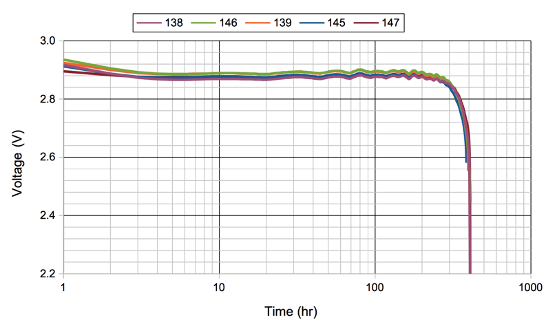
[30-MAR-23] Our first A3047A has been running continuously since the end of January, roughly sixty days. Still running well. Expected lifetime is 76 days.
[06-APR-23] We Have an unencapsulated A3047A1A No69 with no leads. We place it in a Faraday enclosure. We see noise 13, 8, 8, and 6 cnt rms on CH0-CH3 respectively. Note that CH3 is the thermometer channel. In the spectrum of CH0 we see a peak at 64 Hz of 40 cnt, and further peaks at 128 and 192 Hz. These peaks are what create the total noise of 13 cnt rms in CH0. Our CH1 and CH3 do not have sufficient bandwidth to see 64 Hz, but CH2 sees a peaks at 128 Hz and 192 Hz. We remove R1 = 1.0 kΩ and replace with 0 Ω, so as to connect the amplifier and radio-frequency power supplies. Now the peaks at 64, 128, and 192 Hz are twice as large. We turn on our encapsulated A3047A1A and put it in water in our enclosure. We still see the 40-cnt peak at 64 Hz in CH0.
Our transmitter logic is a state machine with sixteen states running off a 1024-Hz clock. In all but one of the states, the SCT transmits a sample. Each time the SCT transmit a sample, the radio-frequency power supply drops by a few tens of millivolts and then recovers over the ensuing millisecond. Sixty-four times a second, however, the state maching enters a new state but does not transmit a sample. The power supply rises slightly more than usual, and it is this irregularity in the power supply voltage that introduces noise at 64 Hz into our amplifiers.
We re-program No69 so that it transmits CH3 at 128 SPS. We still have R1 = 0 Ω. We now have noise 14, 14, 12, and 6 cnt rms (11 uV, 6 μV, 10 μV, 30 mK). Despite eliminating the R1-C6 low-pass filter, we see no switching noise, even in a 32-s interval. Current consumption 139 μA. We go back to CH3 64 SPS and current is 130 μA. We change the CH3 sample rate of the A3047A1A to 128 SPS and drop guaranteed operating life from 76 days to 72 days.
[24-MAY-23] Our first A3047A1A has stopped running. It has been running most of the time since the end of January, which is consistent with a minimum operating life of 76 days.
[28-JUN-23] See here for description of noise-induced oscillation in the Y-amplifier of the A3049AV2, which leads to a DC offset in the amplifier output. The Y-amplifier is identical in form to that the four amplifiers on the A3047BV1. We can fix the problem by dropping resistors R104, R204, R304, and R404 from 10 MΩ to 100 kΩ. Any channel Xn that uses its own reference rather than VC must then have Rn02 dropped to 100 kΩ as well, so that the amplifier presents a symmetric 200-kΩ differential input impedance and 50-kΩ common-mode impedance to the Xn signal.
[13-JUL-23] We examine recordings from two A3047A1A implanted in rats. The EEG (X4) and EGG inputs (X3) inputs are DC-coupled with dynamic range 54 mV and 27 mV respectively. Some of them are saturating some of the time. The ECG (X2) input never saturates.

We propose to increase the dynamic range of the EEG and EGG inputs to 108 mVpp. We replace the all four MAX4464 with OPA369 to reduce offset voltage. We reduce the gain of X3 and X4. We remove the amplifier offset resistors (Rn11). We replace the 10-MΩ on the AC-coupled ECG input with 1 MΩ, following our discovery with the A3049 that the negative side of an AC-coupled differential input must be terminated with 1 MΩ or less to avoid an offset (see here). We drop R404 to 100 kΩ for the same reason: we won't be using the X4− input, but rather we will use GND. To increase the dynamic range of X3 from 27 mV to 108 mV we increase R308 and R307 from 50 kΩ to 200 kΩ. To increase the dynamic range of X4 from 54 mV to 108 mV we increase R408 and R407 from 50 kΩ to 100 kΩ.

We have trouble getting our A3047AV1 to power up correctly, a problem we studied previously. At one point we are unable to power up the circuit correctly with a magnet or battery. We replace R1 with 100 Ω and now the circuit always powers up correctly. Having completed all the above modifications, the result is our first A3047BV2. We program with FV=2, which enables all four inputs with 512 SPS and disables the thermometer. The outputs of the four channels are within ±500 cnt. Noise is 16 cnt rms for all channels. We re-program with FV=1 and create our first A3047A1B.
[19-JUL-23] Firmware P3047A02 now provides uniform sampling, which eliminates scatter noise. With the introduction of uniform sampling, the 4 × 512 SPS version current consumption increases from 245 μA to 248 μA, making the cost 3 μA, or 1.2%, or 0.0015 μA/SPS. With our previous LT1865L converter, the cost was 5%.
[11-AUG-23] We have four A3047BV2 made by modifying A3047BV1. Two work first time. One works after wash and dry. One has displaced logic chip and cannot be programmed. We take pictures of sweep and step response.
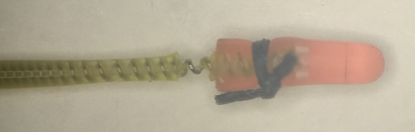
[11-SEP-23] From recordings made at AMU in May with A3047A1As, we obtain these typical ECG waveforms.
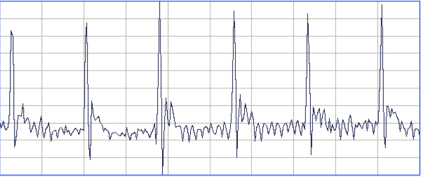
To obtain this recording, our collaborators at AMU cut the two ECG leads to the correct length, stretched the final 10 mm of the wire and insulation, then cut around the insulation 5 mm from the tip. The insulation pulls away from a 1-mm length of wire. They cover the tip with a silicone cap, which they hold in place with a 0/5 silk suture by squeezing the tip onto the lead. We resolve to find a supplier for such caps.
During surgery, they tie the exposed wire to the thoracic muscle with 0/5 sutures. One wire on one side of the heart, the other diagonally opposite.
[25-SEP-25] We have a batch of 7 of A3047A1B-A encapsulated. We turn them all on and put them in warm saline. All voltage signals lie within ±1000 counts. Temperature signals all within a ±20 cnt, which is ±0.1°C. We leave them running overnight. We want to see how their DC offsets vary with time.
[26-SEP-23] Our overnight recording shows all signals stable with the exception of the second hour in which one device shows rumble and then a step in two of its inputs. We note that we put the transmitters in warm saline, which subsequently cooled to room temperature.

Following the rumble we see a sudden full-scale step in the same two inputs, going in opposite directions. No other such events occur. All signals within ±1 mV at all other times.

We now notice that all EEG inputs, which are those with DC-160 Hz bandwidth and dynamic range 108 mV, have 128-Hz noise of amplitude roughly 40 cnt. The entire batch fails QC2.
[27-SEP-23] We take an unencapsulated A3047BV1 and connect 1 Hz, 20 mV to X2 and X3 and look at X4, which is our EEG input. We 125 μV rms noise on X4, shown below. If we turn off sampling with the temperature sensor ADC, and instead sample X3 when we would take temperature samples, the noise disappears. We call the noise "ADC" Noise.

Even if we sample the temperature sensor only once per sixteen sample periods, rather than the usual eight, we get the same noise.
[28-SEP-23] We have two A3047BV1 programmed as A3047A1A. When we load 10 Ω or 0 Ω for R2, the ADC interference drops by a factor of two. We load 0 Ω for R1 and R2 on No0001 and 10 Ω for R1 and R2 on No0004. We apply 20 mVpp to each of X2, X3, and X4 and confirm that input dynamic range is 54 mV, 27 mV, and 54 mV respectively. We connect VC to X− and connect to 0V of our signal source. With 20 mVpp 1 Hz on X2 and X3, we see 50 μV interference on No0001 and 100 μV with No0004. With 20 mVpp on X4 of No0001 we see 80 μV on X2 and 40 μV rms on X3, while for No0004 we see 25 μV and 12 μV.

With 1 mVpp on X2 and X3, we still see the same 100 μV on X4 as with 20 mVpp on X2 and X3. The noise appears when the signal exceeds VC. We return to 20 mVpp and offset the input signal downwards. We see the noise appearing when the the X3 amplifier output rises above VA/2. That is, when the most significant bit of the the U5 readout it HI, we have a problem. We reduce the number of SCK falling edges we deliver to U7 during readout from 24 to 28. Our ADC noise problem vanishes. The correct number of edges for readout only is 18. The 24 edges provoke an autocalibration on power-up. We had concluded from an examination of the ADS7052 data sheet that 24 edges would have no effect at any time other than power-up, but this proves to be incorrect. We introduce a power-up calibration flag into the logic, by using the SET function for a logic pin output. When CAL is set, we deliver 24 edges to provoke calibration, and after clear CAL so we deliver only 18 edges on subsequent readouts.

Here we see a thermometer readout and transmission, followed by the CAL flag being cleared. When we apply 20 mVpp to X2 and X3 we see 45 μV noise on X4 with No0001 and 30 μV on No0004. We restore R2 to 1 kΩ on both boards. Total noise on X4 with 20 mVpp on X2 and X3 is now 25 μV for both No0001 and No0004. We now have P3047A03.
[11-OCT-23] We have two A3047A1B poaching. After five days, all three analog inputs on one device start to drift out of range and jump. A few days later, this device stops transmitting. We dissect and diagnose a corroded capacitor. The other device is performing well.
[02-OCT-23] A3047A1B number A1B235.37 failed yesterday after running for 64 days in water at 60°C, showing no degradation of its amplifiers until the battery neared exhaustion at 62 days. We place another A1B-A in 50 ml of 1% saline and see reception from the transmitter drop dramatically. We cannot obtain reception from our 4-antenna TCB setup in a Faraday enclosure. Consulting our work on reception in and out of saline, we see that dramatic changes in output power are a characteristic of the RF output when we have no antenna protection network, as is the case for the current A3047 circuit. We must update to add the 15pF-100Ω-15pF protection network.