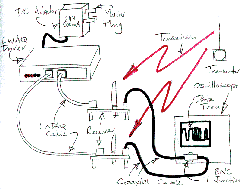
| On-Off Switch | Power Supplies | Logic Chip | Oscillators | Transmission | Transmitting Antenna | |
| Board Trimming | Battery Life |
| Receiving Antenna | Input Amplifier | Band-Pass Filter | Downshifter | Low-Pass Filter | Limiting Amplifier | |
| Demodulator | Output Amplifier |
In our Technical Proposal for the Subcutaneous Transmitter, we layed out our plan for developing a transmitter small enough to be implanted in the body of a rat, fast enough to transmit four hundred sixteen-bit data samples per second, powerful enough to be detected at a range of three meters, and efficient enough to operate for three months on a lithium battery. We divided our development into four stages, each of which we committed to complete within a number of weeks of receiving payment for the previous stage
Open Source Instruments (OSI) submitted its Technical Proposal in November 2004, together with one Miniature Transmitter (A3001D) and one Downshifting Receiver (A3001B). This completed Stage One of development. OSI invoiced ION (Institute of Neurology) for £3000 and received payment on 18 January 2005.
On 16th February 2005, Kevan Hashemi, President, OSI, visited Matthew Walker at ION and brought him four Transmitters with On-Off Switches (A3002), which Kevan demonstrated along with the Downshifting Receiver (A3001B). On 26th April 2005 OSI shipped two Transmitters with Logic Chips (A3004) and two Demodulating Receivers (A3005) to Matthew at ION by DHL. These final circuits meet our optimistic performance targets, and complete Stage Two of development. On 28th April 2005 OSI sent an invoice by airmail to ION for £5,000 as agreed upon for the completion of Stage Two.
According to the schedule layed down in its Technical Proposal, OSI Inc. should have delivered its Dummy Transmission Circuits within eight weeks of receiving payment for its Technical Proposal. Even allowing for the time it took for a United Kingdon check to clear through the United States banking system, these circuits were due on 18th March 2005. As it is, OSI shipped them on 26th April, five weeks late. We did, however, obtain permission from Matthew Walker to delay shipment by several weeks because we believed that in doing so we could supply circuits far superior to the ones we had available in March. Therefore, we believe we are justified in invoicing ION in full for Stage Two of development, even though its completion is at least five weeks behind schedule.
In the following sections we describe the performance of the new transmitters and receivers. We suggest a program of tests for Dr. Walker to perform with them at ION, and we discuss our plans for the next stage of development.
Our Transmitter with On-Off Switches (A3002) came in three varieties. All were made on a two-layer printed circuit board without a ground plane. The first variety (A3002A) was 80 mm square, with a quarter-wave square loop antenna around the edge of the circuit board. The transmitter sat at the center of the board, and the board had no ground plane. The loop antenna worked well, and transmitted measurable 1-GHz RF (radio frequency) power to our Downshifting Receiver (A3001R) at a range of five meters through air. The absense of a copper ground plane in the circuit board meant that the loop antenna operated freely in the surrounding air.
The second variety of (A3002B) was 18-mm square with a hole in the circuit board for a quarter-wave antenna. Equipped with a 75-mm antenna in air, this variety transmitted measurable power at a range of five meters also. Equipped with a 15-mm antenna, and enclosed in a latex glove finger, it transmitted measurable power from a cup of water at a range of three meters. Matthew Walker reported transmission through a silicon coating from within a cup of water at a range of three meters also.
The third variety (A3003C) was 18-mm square with a square loop antenna wrapped around the edge of the board. This variety was intended for use in a cup of water. But it appeared to perform no better in a cup of water than out. In either case, it transmitted measurable power over no more than one meter. We concluded that the battery, which sits in the middle of the transmitter board and has a conducting metal case, rendered the loop antenna ineffective.
The failure of the 18-mm square loop antenna led us to conclude that we should choose a protruding quarter-wave antenna for the next generation of transmitters. We knew that a square loop antenna around the edge of the board would transmit no power in the presence of a circuit board ground plane. The fact that the antenna protrudes from the board means that the printed circuit board can have a ground plane, which simplifies the circuit board layout.
The A3002 used the smallest surface-mount reed switch in the world (RI80SMD) to turn off a MOSFET switch (2SJ0536) when we bring a magnet near the switch. When we remove the magnet, the MOSFET switch turns on, and the A3002 begins to transmit RF power. We cannot use the switch to turn the A3002 on and off directly because the switch closes when the magnet is near, so using the switch directly would require that we put the magnet near the transmitter during operation.
The switch worked well, but we found it awkward to keep the magnet attached to the transmitter when we set the transmitters aside. When we demonstrated the A3002 to Ralf Schoepfer, he suggested that we use the logic chip on the next generation transmitter to implement a push-button on-off switch, so that when you close the switch and open it, the transmitter turns on, and when you repeat the process, it turns off again.
In our Technical Proposal, we presented a block diagram of our proposed subcutaneous transmitter. The Transmitter with Logic Chip implements this proposed transmitter, but without the analog input amplifiers and analog-to-digital converter. It is designed to prove that we can transmit data out of a rat at 400 samples per second, and to determine the power consumption of this transmission process. The addition of analog circuits in Stage Three will take some time and effort, but we expect no technical challanges from the analog design and construction.
Our Transmitter with Logic Chip (A3004) uses a programmable logic chip and a low-power clock oscillator to transmit a thirty-bit data word by radio frequency modulation five hundred times a second. It's current consumption from its 3-V lithium battery while the transmitter is active (transmitting five hundred times a second) is roughly 60 μA, and when idle (not transmitting) it is roughly 15 μA. It transmits measurable power through air at ranges up to 15 m. Measurements we performed with our Demodulating Receiver (see below) suggest that the transmitter's maximum data transmission rate is 6 MBits/s. It transmits its thirty-bit data word in 4 μs. The data word contains an eighteen-bit counter value whose most significant bit changes every four minutes.
The A2004's on-off switch consists of a normally-open reed switch in series with a 10-KΩ resistor (S1 and R3 respectively towards the bottom of the schematic). Every two milliseconds, the logic chip checks to see if the reed switch is closed. This check adds less than a tenth of a microamp to the quiescent current of the transmitter. You can look at the logic chip's firmware to see how the transmitter's programmable logic chip performs this check, and implements the on-off switch logic. When the transmitter is active, if the switch closes and opens again, the transmitter becomes idle. When it is idle, if the switch closes and opens again, the transmitter becomes active.
The on-off switch turns on and off the transmitters radio-frequency data transmission, but does not turn on and off the logic and low-frequency oscillator chips. These continue to draw roughly 15 μA even when the transmitter is off. Instead of on and off, we speak of the transmitter being active and idle. When idle it consumes 15 μA, when active it consumes 60 μA.
There are two ways to close and open the switch. One is to bring a magnet close to it for a moment. This will work half the time, and the other half it wil cause two open-close cycles, which will leave the transmitter in the same state it started. Another way to close the switch for a moment is to bang the transmitter on the table, or drop it on the floor. Banging the switch or dropping it carries the risk of shattering the glass of the reed switch, so we do not recommend you make a habit of activating and de-activating the transmitter by banging or dropping it.
Regardless of how you close and open the reed switch, you need to have a receiver set up to detect active transmission or else you will not be able to tell for sure if your efforts to activate or de-activate the transmitter have been successful.
If you want to be sure that the transmitter remains off, you can de-activate it and fasten a magnet to its reed switch, so that the switch remains closed. Stray magnetic fields and mild shocks will not be able to open the reed switch and activate the transmitter. When we shipped two A3004s to the UK from the US, however, we deactivated them, wrapped them in bubble wrap without magnets, and put them in a metal box so that no signal would escape even if one of the transmitters did become activated in transit.
A lithium battery, the BR1632-1HF from Panasonic (B1 in the schematic), provides power to the transmitter. The BR1632 produces 3 V when new, and has capacity 120 mA-hr, which means that the area under the graph of its output current versus time is 120 mA-hr. That is not to say that you can draw 120 mA from it for one hour, because the batter also has an output resistance of around 100 Ω. When we draw 10 mA from the battery, this 100-Ω resistance drops the battery voltage from 3 V to 2 V. When the transmitter is in the act of transmitting a 4-μs burst of modulated radio-frequency power, its current consumption jumps up to around 10 mA. We don't want the transmitter's supply voltage to drop down to 2 V during power transmission, so we C1, a 1-μF capacitor, acts as a short-term battery. The 10-mA consumption for 4 μs causes the voltage on the capacitor to drop by only 40 mV. The battery spends the next 2 ms charging up the capacitor with a steady input of 20 μA.
The battery voltage supplies all parts of the transmitter directly, with the exception of the programmable logic chip, which requires 1.8 V. This low-voltage supply allows the logic chip to consume only 10 μA quiescent current. We presume that at higher supply voltages raise the quiescent current dramatically because charge begins to leak through field effect transistor gate oxide by quantum tunneling. The A3004 uses the MAX1726EUK18 to produce a stable 1.8-V supply from the battery voltage, while consuming only 2 μA of quiescent current itself.
The ispMACH4064Z from Lattice Semiconductor (U2 in the schematic) is a programmable logic chip in a 48-pin TQFP (thin quad flat-pack) surface-mount package. This package takes up a 10-mm by 10-mm area on the A3004 circuit board. The same chip comes in a 56-pin BGA (Ball Grid Array) that takes up only a 6-mm by 6-mm area. We will use the 56-pin BGA in the final transmitter design, but for this design we wanted to stick with a package familiar to us, so that we could separate the challanges of assembly from those of data transmission.
We program the logic chip through an industry-standard JTAG programming port. Four logic signals pass from the logic chip to an eight-way single-row plug (P1 in the schematic) on the programming extension of the transmitter circuit board (see drawing in schematic). We connect a programming cable (available from Lattice Semiconductor) to P1. Our programming cable plugs into a Windows PC parallel port, and we run Lattice Semiconductors free ABEL-language compiler and chip programming software on this Windows PC. We define the logic functions of the chip in a text file written in a language called ABEL. The ABEL compiler converts the ABEL text file into an industry-standard JEDEC file. A JEDEC file is also a text file, but it does not make much sense to a human reader. The programming software takes the JEDEC file and uses it to program the logic chip with the functions defined in the original ABEL file. The configuration of the logic chip is not quite a computer program, but nor is it hardware, since it can be changed. It's somewhere inbetween, which is why we call if firmware. The A3004 Manual provides links to the existing firmware. You can look at the ABEL files, and also the JEDEC files.
Once we have programmed the chip through P1 and tested the transmitter, we cut the programming extension off, leaving the 18-mm square miniature transmitter with its antenna sticking out. In the photograph below, you can see the logic chip on the top side of the board.
According to its data sheet, the ispMACH4064Z consumes only 11 μA of quiescent current when idle, plus another 10 μA for each internal logic gate switching at 1 MHz. When the transmitter is idle, it is counts transitions of the 32-kHz oscillator (U4 in the schematic), which means we have (for a long binary counter) the equivalent of two logic gates switching at 32 kHz, for an additional current of less than 1 μA. With the transmitter idle, the data sheet claims implies that the logic chip will consume around 12 μA. We found this claim hard to believe, but it turned out to be true.
The transmitter needs two oscillators: a slow one and a fast one. The slow one must consume only a few microamps, because it runs all the time, and allows the logic chip to figure out when to transmit its data bursts. The fast one can consume several milliamps, but is must start up immediately and stop immediately. It runs only during power transmission. The logic chip uses the fast oscillator to time the modulation of its outgoing radio-frequency transmission.
Our low-frequency oscillator is the OV1564C2 from Golledge (U4 in the schematic). According to its manufacturer, the OV1564C2 produces a 32.7680-kHz square wave accurate to better than ±1 Hz while consuming 1.5 μA (typical, maximum is 2 μA). As with the logic chip, we found this claim hard to believe, but they turned out to be correct. Our P3004A01 firmware performs no radio-frequency transmission, but counts the 32-kHz clock and forwards it to the programming extension, so that we can look at it with an oscilloscope. We inserted a current meter between the battery and the circuit and measured a current consumption of 16 μA.
If we assume the logic chip consumes 12 μA, and the regulator 2 μA, we are left with 2 μA for the 32-kHz oscillator. That's close enough, as far as we are concerned.
We implement the fast oscillator in the logic chip, by taking several logic gates, connecting them in a sequence, inverting the output of the final one, and feeding it back to the input of the first one. If you imagine a logic HI propagating around the ring, it turns into a LO when it passes through the inverter, and travels around the ring again, before turning into a HI again, and so on. If you look at any one of the gates, its output oscillates in a symmetric square wave. The half-period of the square wave is equal to the propagation time around the loop. The propagation time of one gate in the ispMACH4064Z is roughly 2 ns, so we expect a five-gate ring oscillator to oscillate with period 20 ns, or frequency 50 MHz. All we have to do to turn off the ring oscillator is disable one of the gates. All we have to do to turn it on again is enable the same gate.
With five gates running at 50 MHz, we expect the ring oscillator to consume roughly 2.5 mA. We found that the ring oscillator together with some counters and state machines consumed 4 mA. With three gates running at 80 MHz, the power consumption is also 4 mA. The power consumption of a ring oscillator with an arbitrary number of gates is the same, because we have one gate transition every 2 ns around the ring, which is equivalent to a single gate oscillating at 250 MHz. Our P3004A03 firmware, which transmits 30-bit data bursts every 2 ms, uses a three-gate ring oscillator. With the ring oscillator and its counters and state machines consuming 4 mA for 4 μs once every 2 ms, we add 10 μA to our quiescent current consumption.
The A3004 transmits a thirty-bit number in a 4-μs burst once every 2 ms. During the burst, the A3004 sends the thirty bits one after another. To send a binary 1 (one), the A3004 transmits radio frequency power at 950 MHz. To send a binary 0 (zero), the A3004 transmits power at 875 MHz. The receiver, meanwhile, which we discuss below, responds to power in the pass-band of its SAW filter, which is roughly 930 MHz to 970 MHz.
Our source of radio-frequency power is a MAX2624 voltage-controlled oscillator, or VCO (U3 in the schematic). The MAX2624 comes in an MSOP-8 package (miniature small outpline plastic) and provides a !SHDN (disable shutdown) input and a TUNE (output frequency adjust) input. Its output is a sine wave of frequency 875 MHz to 1050 MHz, depending upon the TUNE input. We measured the response of the output amplitude and frequency to !SHDN and TUNE in one of our Modulating Transmitter feasability study.
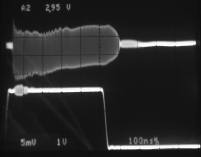
When !SHDN is 0V, the MAX2624 consumes 0.1 μA (typical, not maximum). When we drive !SHDN to 3 V with our logic chip, the MAX2624 consumes 8 mA (typical, not maximum) at room temperature. We see from Figure 1 that the VCO generates radio-frequency power within 100 ns of !SHDN being driven to 3 V, but it is not clear from the oscilloscope trace whether the frequency of the generated power is stable after so short a time.
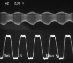
Figure 2 gives us an idea of the time constant of the MAX2624's output frequency in response to a step change in TUNE input. It appears that the time constant is roughly 100 ns. The MAX2624's frequency range is 875 MHz to 1050 MHz, as shown in Figure 3. According to the figure must drive TUNE to 0 V for an output frequency 875 MHz, and 1 V for 950 MHz.

Figure 3 is a typical curve, not guaranteed by the manufacturer. It may be that some MAX2624 chips transmit outside our receiver's 930-MHz to 970-MHz pass band, in which case we would need to change the voltage on the TUNE input for the transmission of a binary 1. But we will not have to change the voltage on TUNE for a binary 0, because our receiver assumes that an absence of power at 950 MHz means a binary 0. Even if the MAX2624 transmits at 900 MHz or 860 MHz instead of 875 MHz, it is still transmitting well outside the pass-band of the receiver. Our concern, then is with the transmission of 950 MHz power, not with the transmission of 875 MHz power.
There are two ways to modulate the MAX2624's output that will work perfectly well with our receiver. One is to set the TUNE input to a constant value, and turn on and off the 950-MHz radio-frequency power with !SHDN. We tried this modulation method, and it works fine for bit rates below 2 MB/s (each bit takes 500 ns). The second method is to drive !SHDN to 3 V and turn on 950-MHz radio-frequency power with TUNE. We tried this modulation method also, and we were able to attain bit rates of up to 10 MB/s. Our objective is to minimise the power consumption of the transmission. If we use !SHDN to modulate the output, the VCO consumes 8 mA only when transmitting a binary 1. At 2 MB/s data rate, and assuming random data values, modulation by !SHDN halves the VCO power consumption compared to modulation by TUNE. But when we modulate with TUNE, we need only 100 ns to transmit each bit. We can transmit a binary 0 and 1 in less time than it takes to transmit a single binary 1 using modulation by !SHDN.
The A3004 with firmware P3004A03 modulates the VCO output frequency using TUNE, and relies upon the receiver's ability to reject 875 MHz to distinguish between binary 1's and 0's. We take a 1.8-V output from the A3004's logic chip (U2), and pass it through two resistors to create 1 V. As the logic chip output changes from 0 V to 1.8 V, the TUNE input changes from 0 V to 1 V. The VCO output frequency should change from 875 MHz to 950 MHz. The time constant of this change is 100 ns when we drive the TUNE input with a low-impedance voltage source, as shown in Figure 2. But in the A3004 we drive TUNE through R1 and R2, and we find that the capacitance of the TUNE input, combined with these resistors, gives us a time constant of 200 ns. We add C6 of 68 pF to the ciruit to cancel the effect of the TUNE input capacitance, and so obtain a 100-ns time constant while avoiding wasting current through smaller values of R1 and R2.
If the VCO consumes 8 mA for 4 μs every 2 ms, we expect it to add 16 μA to the transmitter's active current consumption.

Figure 4 shows the thirty-bit data word transmitted by the A3004 five hundred times a second. The first four bits of the transmission are always ones. The fifth bit is a zero. The next eighteen bits are the top bits of a twenty-four bit counter that counts cycles of the A3004's 32-kHz oscillator. The top bit changes every four minutes. Following the counter bits are six zeros, and then a single one.
The first four ones of the transmission guarantee that the transmitter has come out of shutdown and the receiver has had time to respond to the power it receives at 950 MHz before the first zero arrives. The first zero give us a permanent feature in the data word, by which we can determine the positions of the other bits. You can trigger on the rising edge of the receiver output, but the duration of the positive pulse caused by the four ones depends upon how long it takes the VCO to come out of shutdown and settle upon a 950 MHz output. The relationship of the first falling edge of the transmission, however, depends only upon the frequency of the ring oscillator. The six zeros at the end of the transmission give space around the final one. This solitary one shows us both the rise and fall times of the combined transmitter and receiver response.
The A3004 antenna is a piece of wire sticking out of the board. We use solid-core wire with plastic insulation. We started with a 120-mm length of wire and measured the range in uninterrupted air over which our receiver could detect data transmission from the antenna. This range reached a maximum of fifteen meters when the antenna was 80 mm long. Our 950-MHz carrier frequency travels roughly 30 cm/ns through air, and has period roughly 1 ns. A quarter-wavelength in air is close to 80 mm. Because the optimal length of our protruding piece of wire is a quarter-wavelength, we believe we are justified in calling it a quarter-wave antenna, even though the piece of wire is not accompanied by the infinite flat ground plane that the theory of quarter-wave antennas requires.
We determined the optimal antenna length both with the programming extension attached and detached. The ground plane associated with our antenna decreases in area by 70% when we cut off the programming extension, and yet we observed no change in the optimal antenna length as a result of removing the extension. It may be that the power transmitted by the antenna decreases when we cut off the programming extension, but we still get the maximum power from an 80-mm antenna. We conclude that the optimal antenna length is a function only of the speed of the electromagnetic wave travelling down the antenna.
We cut the programming extension off the board with a hand-held rotating wheel cutter. The cutting takes only a minute, but generates unpleasant fiberglass dust. Before we cut the extension off, we disconnect power from the transmitter, so as to avoid shorting any of the logic chip's programming or test outputs to the power supplies. We do not know for sure that we will damage the logi chip by cutting with the power on, but we did not take any chances. Once we have removed the extension, the logic chip cannot be re-programmed.
Our transmitter's idle current consumption we measure to be 15 μA, and this agrees with the our component data sheets. The 32-kHz oscillator takes 2 μA, the logic chip takes 11 μA, and the regulator takes another 2 μA. The ring oscillator and associated logic consumes 5 mA for 4 μs once every 2 ms. Capacitor C1 supplies this higher current during the 4 μs of activity. The battery can re-charge C1 with a steady current of 10 μA, so the ring oscillator and associated logic add 10 μA to the battery current. The VCO and its radio-frequency output consume roughly 8 mA, assuming a 50-Ohm load at the VCO output. This 8 mA, occuring for 4 μs out of every 2 ms, adds another 16 μA to our expected battery current. We expect the total active battery current to be around 40 μA.
When we insert a current meter between the battery and the transmitter, it reads between 42 μA and 48 μA, depending upon the transmitter.
Let us assume that the active battery current is 45 μA. According to its data sheet, the capacity of the BR1632-1HF battery is 120 mA-hr, so we are confident that the A3004 with firmware P3004A03 will run for almost four months on a single battery. We have not had a chance to observe this battery life directly. We have a transmitter that has been running since 15th April, 2005 in lab, starting with a battery that was almost fresh. We will see how long it lasts.
Our Demodulating Receiver (A3005) uses a SAW (surface acoustic wave) filter to select radio-frequency signals in the frequency range 930 MHz to 970 MHz. It produces a voltage output that indicates when power received in this range exceeds that generated by thermal noise in the receiver's input amplifier. The rise and fall time of this voltage output in response to the sudden arrival or disappearance of RF power in the range 930 MHz to 970 MHz is 50 ns. The receiver is capable of receiving data at up to 20 MBit/s, which is several times faster than our transmitter's maximum data rate.
Figure 5 shows a single receiver with its output displayed on an oscilloscope. The antenna is the black rod sticking straight up from the circuit. It is a dipole antenna designed to work at 900 MHz, part number ANT-916-PML from Digi-Key. The antenna works well enough at 950 MHz. It provides a mounting thread, a coaxial cable for connetion to our circuit, and a joint at the base. The joint allows you to change the orientation of the receiver. If we mount the receiver circuit board parallel to a wall, we can rotate the antenna so that the dipole is vertical.

A dipole antenna is most sensitive to signals arriving in directions perpendicular to its length. Provided our transmitters lie close to the plane defined by these directions, the antenna will be more sensitive to our signals than to interfering signals arriving from above or below. The relative sensitivity to signals arriving from different directions is, in fact, the only way we can reject interference signals in favor of our transmitter signals. Our dipole antenna ignores signals coming from directly above or below, but accepts signals coming from every diretion on the same floor. We find that we receive some interference from anonymous 950-MHz sources, but it is hardly above the level of thermal noise.
If we find that the dipole antenna provides inadequate rejection of interfering signals, we could place a more complicated array antenna that accepts signals only in a 90-degree aperture. We could put this antenna in the corner of our laboratory so that it accepts signals arriving across the laboratory benches, but ignores signals from the other directions of the compass, as well as from above and below. Such antennas are readily available for under $100.
The antenna's impedance is close to 50 Ωs, so we can connect it directly to our 50-Ω amplifier chain with minimal loss of signal power. In the absence of interfering signals on the antenna, the sensitivity of our receiver will be limited by the thermal noise. If our input amplifier were perfect, it would introduce no thermal noise of its own, and the only thermal noise our signal would have to compete with would be that of the amplifier's input impedance. But no amplifier is perfect. Our amplifier is the ERA-3SM from Minicircuits (U1 in the schematic). The ERA-3SM has a gain of 20 dB (multiplies the signal voltage by ten) and a noise figure of 3.8 dBm. The noise figure means that the amplitude of the amplitude of the noise at the output of the amplifier will be 50% higher than the amplitude at the output of a perfect amplifier.
The thermal noise at the input of U1 that will affect our receiver output is a function only of the bandwidth, B, measured in Hertz, to which our receiver is sensitive. As we will see below, our receiver is sensitive only to frequencies between 940 MHz and 960 MHz. Thermal noise power, measured in Watts, is 4BTk, where T is absolute temperature and k is Boltzmann's constant, 1.4 × 10⁻²³ J/K. The thermal noise power in a 40-MHz bandwidth is 0.4 pW. Our amplifier's noise figure is 3.8 dB, so the effective noise in our receiver's pass-band at the input to U1 is 1 pW, as marked next to the base of the antenna in the schematic. Across U1's 50-Ω input impedance, this 1 pW appears as a random voltage of amplitude 10 μV rms (root mean square). At the output of U1, this same noise has amplitude 100 μV rms.
Immediately following our low-noise input amplifier is our surface acoustic wave (SAW) filter, which acts as the receiver's band-pass filter. A SAW filter works by transmitting the oscillating energy of an electrical signal across the surface of a piezoelectric crystal in the same way that water waves travel across the surface of the sea. We invite you to look at our Filter Design Guide to see how comb-like electrodes on each end of the crystal transmit and receive waves within a narrow frequency band. It is almost impossible to build a bass-band filter out of inductors, resistors, and capacitors with the same precise, sharp attenuation at the edge of the pass-band that we can acheive with a SAW filter. The purpose of our receiver design is to make good use of the SAW filter's impressive properties.

Our SAW filter is the DSF-947.5 manufactured by ECS. It's center frequency, as you can see in Figure 6, is 947.5 MHz, which we tend to round to 950 MHz in our discussion. Its pass-band is roughly 930 MHz to 960 MHz. This 40-MHz pass band is only 4% of the center frequency, and yet signals a few Megahertz outside it are attenuated by 30 dB. Such a response is remarkable to those of us who have built pass-band filters out of discrete passive components, but it is not remarkable by SAW filter standards. There are SAW filters available with center frequency 950 MHz and a 1-MHz pass-band. We chose the 40-MHz pass-band because we want the SAW filter to stop ringing quickly whe we remove our 950 MHz power. The impulse response of an infinitely tight pass-band filter is a sinusoidal wave of the pass-band center frequency that persists forever. If our SAW filter had a 1-MHz bandwidth, then it would take several microseconds for it to stop ringing at the center frequency after it had been excited by a center-frequency input. Because our SAW filter has a 40-MHz bandwidth, it will stop ringing within a few tens of nanoseconds. Conversely, when the 950 MHz power appears at its input, the SAW filter output will respond within a few tens of nanoseconds.
We can observe, with our 300 MHz oscilloscope, the 950-MHz output from our SAW filter, but the signal is greatly attenuated. To measure the frequency response of the SAW filter, we looked at the IF (intermediate frequency) output from our IF filter (L7 in the schematic). In the following photograph, our function generator provides a 0-V to 2.4-V triangle wave for one of our Modulating Transmitters (A3001A). The triangle wave drives a MAX2624 VCO on the A3001A. Figure 7 shows the apparatus.

The VCO frequency sweeps from 875 MHz to 1050 MHz as the triangle wave sweeps from 0 V to 2.4 V. We trigger the oscilloscope off the triangle wave. Figure 8 shows the output from L7.

We know from the VCO's data sheet that its output should be 950 MHz when its TUNE input is 1.0 V. The center of our SAW filter's frequency response coincides with a TUNE voltage of 1.1 V, although the peak response corresponds to a TUNE voltage of 1 V. We assume that the SAW filter is more accurate than the VCO, so the pass-band we see in the oscilloscope trace corresponds to the band 927.5 MHz to 967.5 MHz, which we round to 930 MHz to 970 MHz.
You will find another view of the SAW response in Figure 12, where we see the IF frequency during data transmission. The IF signal is larger at the beginning of a burst of 950-MHz power. This is because the transmition frequency passes through the peak response of the SAW filter on its way to its final settled frequency. We found that the SAW filteres varied. Some had peak response in the middle of their pass band, others had peak response to one side of the pass band. The transmitters vary also. Their output frequency at 1-V input might be 10 MHz away from the nomonial 950 MHz.
We pass the output of our SAW filter through another amplifier, an ERA-1SM from Minicircuits (U2 in the schematic). The ERA-1SM has gain 10 dB. On its way to the output of U2 (RF signal in the schematic) the 0.4 pW thermal noise at the input of U1, is increased by 3.8 dB through noise generated by U1 itself, amplified by the 20-dB gain of U1, attenuated by the 4-dB pass-band insertion loss of L5, and amplified by the 10-dB gain of U2. The noise power on our RF signal is therefore 400 pW. Across the 50-Ω input impedance of L6's RF input, the noise appears as a random signal of amplitude 150 μV.
If the noise on our RF signal has amplitude 150-μV, we hope our 950-MHz signal has amplitude at least three times higher, or roughly 500 μV rms. Our signal will be ten times more powerful than our noise. We will mistake noise for signal less than 1% of the time. If our antenna signal is 10 pW, which it appears to be at a range of 20 m in air our receiver will have no trouble rejecting 875-MHz power by means of the 40-dB relative attenuation of 875 MHz with respect to 950 MHz through our SAW filter. But suppose our antenna signal is 100 nW at 875 MHz. Even after the SAW filter, our RF output will now be 500 μV rms. We will be in danger of interpreting the strong 875-MHz reception as a weak 950-MHz reception.
We see that the receiver has a maximum operating range dictated by thermal noise, and a minimum operating range dictated by the ratio of its sensitivity to 950 MHz and 875 MHz. It turns out that the minimum range is two meters or more. To decrease this minimum range, we increase the ratio of the receiver's sensitivity at 950 MHz to its sensitivity at 875 MHz with a low-pass filter (L7) and 50-MHz resonant tank circuits (C22/L8 and C26/L9).
We introduced the principle of downshifting in our Downshifting Receiver (A3001B) report. The A3005 downshifter is almost identical to that of the A3001B. A MAX2624 acts as the local oscillator (U4 in the schematic). Its output is amplified by 10 dB by U5, and fed into the mixer, L6, as the LO input. Our RF signal enters the mixer at the RF input. The output from L6 contains three frequencies: the sum of the LO and RF frequencies, their difference, and some LO feed-through. The difference between the LO and RF frequencies we call the intermediate frequency, or IF. The mixer introduces a 10-dB loss in our signal path, and we make this up immediately with the 10-dB gain of U3.
The TUNE input of the local oscillator is connected to a preset resistor, VR1. We drive our Modulating Transmitter's TUNE input with 1.1 V, so that the frequency it transmits to our receiver is in the center of the SAW filter's pass band, and therefore close to 950 MHz. We measure the intermediate frequency, IF, at the output of L7 with our oscilloscope. We adjust VR1 until the IF frequency is 50 MHz, at which point we assume the LO frequency is 1000 GHz because the RF signal is 950 MHz.
Our low-pass filter serves two purposes. First, it rejects the high-frequency components of our downshifter output (the sum of the LO and RF frequencies, as well as the LO feed-through). Second, it helps reject the IF signal when our antenna receives 875-MHz power from our transmitter. The transmitters send a binary one (1) by radiating power at 950 MHz, and a binary zero (0) by radiating power at 875 MHz. When our RF signal is 950 MHz, the SAW filter passes the signal with only slight loss, and the signal emerges as a 50 MHz IF from the downshifter. When our RF signal is 875 MHz, the SAW filter attenuates the RF by at least 40 dB more than it does a 950 MHz signal (see data sheet). Nevertheless, some 875 MHz RF power makes it through the SAW filter to the mixer (L5), and emerges as a 125-MHz IF signal. Our low-pass filter, L7, attenuates signals above 95 MHz. It is the SCLF-95 from Minicircuits. A 50-MHz IF passes through L7 with a slight loss, but a 125-MHz signal is attenuated by 20 dB. As the RF signal changes from 950 MHz to 875 MHz, the IF power at the output of our 95-MHz low-pass filter drops by at least 60 dB.
The noise on RF is downshifted along with the signal, and appears on IF as a random combination of 30-MHz to 70-MHz sinusoids with amplitude 150 μV rms. With 10 pW at 950 MHz on our antenna, IF output will be a 50-MHz sinusoid of amplitude 500 μV rms. With 100 nW at 875 MHz, the IF output will be a 125-MHz sinusoid of amplitude 50 μV rms. We see that we are no longer in danger of mistaking a 100-nW 875-MHz signal for a weak 950-MHz signal.
You will find an oscilloscope display of the IF signal during data reception in Figure 12.
Our Limiting Amplifier provides a self-limiting gain of 50 (34 dB), and consists of two OPA699 limiting op-amps (operational amplifiers) in series (U7 and U8 on page two of the A3005 schematic, where they are called "OP699"). The input to the limiting amplifier is the output of our low-pass filter, but coupled through a capacitor so that the AC (alternating current) IF signal is superimposed upon the amplifier's common-mode voltage (VCM in the schematic). The OPA699 is a 1-GHz bandwidth op-amp that limits the amplitude of its output to VCM±1 V. Unlike normal op-amps, the OPA699 does not get stuck for a while when it's output reaches its upper or lower voltage limit. The OPA699 output is designed to stop going higher than a postive limit, and lower than a negative limit, but to come back towards VCM as soon as the input signal is small enough to warrent such a move.
The noise on IF enters the Limiting Amplifier with amplitude 150 μV rms, and emerges with amplitude 7 mV. With a 10-pW 950-MHz signal on our antenna, the limiting amplifier's output will be 25 mV. The output for a 100-nW 950-MHz signal will be 1 V, not 250 V. The frequency of the output will in both cases be 50 MHz.
If we allow 1 μs per bit, the SAW filter and Low-Pass Filter reject 875-MHz well enough to operate with transmitter ranges 40 cm to 20 m. But when we allow less than 1 μs, we discover that the frequency we receive from the transmitter does not change immediately from 875-MHz to 950-MHz, nor does it change with a smooth time-constant. Instead, we see power at the low end of our pass band for several hundred nanoseconds after the transition from 950 MHz to 875 MHz has begun. If the receiver is to operate with only 200 ns per bit or less, we improve its rejection of frequencies just outside its pass-band. We do this with a pair of LC resonant tank circuits (L8/C22 and L9/C26 in the schematic), one for the input to each of our demodulating amplifiers. We need only one such tank circuit in theory, but in we added the tank circuit to the receiver design only after we had laid out the printed circuit board, and it turned out that the most convenient way to add the tank circuit response was to put a capacitor and inductor in parallel at each of the demodulator inputs. A 100-pF capacitor and 100-nF inductor in parallel presents a high impedance at 50 MHz, and a much lower resistance at other frequencies. With these particular components, the impedance at 50-MHz is 1 kΩ. Figure 9 shows the demodulated output from the limiting amplifier versus RF frequency without the tank circuits, and Figure 10 shows the same response with the tank circuits.

As you can see, the response without tank filters is flat across the center of the pass band, but with the tank filters the response falls off towards the edge of the pass band. We found that this narrowing of the response allowed us to identify a transition from 950 MHz to 875 MHz within a hundred nanoseconds of the transition commencing, at ranges as small as 50 cm.

We make a full-wave demodulator out of two more limiting op-amps (U9 and U10 in the schematic). This time we tie the bottom limit input of each amplifier to VCM, so that the outputs are clipped off below VCM. Once cuts off the negative cycles of the amplified IF signal, and the other inverts the IF signal and cust off the negative cycles of the inverted signal.
We add these two demodulator outputs together with U6, and so produce the full-wave rectified receiver output. We place a 50-Ω resistor in series with the output so that we can connect two receiver outputs together and see the average of the two at the output of each. Figure 10 gives the frequency response of the receiver output for transmitter range 1 m.
As we discussed in our Technical Proposal (section on the miniature transmitter), the signal received by a single antenna will drop dramatically for certain precise combinations of orientation and location of the transmitter. We refer to these precise combinations as reception dead spots. With the transmitter in a reception dead spot, we move the receiver antenna by 30 cm to one side, and our signal re-appeared. The dead spots are a function also of the precise receiver position. We did not have to change the orientation of the receiver, only slide it sideways across the table upon which it rested. We concluded that combining the outputs of two receivers would improve our immunity to such dead spots, because it would be unlikely that the transmitter would be in a dead spot for both receivers at once.
With the dual receiver, we obtain robust data reception for ranges 50 cm to 8 m, which is the diagonal length of our laboratory. At greater ranges, we must walk out of our laboratory and into the neighboring laboratory, and when we do that, our signal strength drops dramatically, as we will see in the following section.
We obtained the body of a baby rat from a colleague and implanted a transmitter under the skin of its back. We placed the transmitter near its head (which was missing), and ran the antenna down towards its tail. With a 40-mm antenna, which was the longest we could fit down the spine of the baby rat, we received a strong signal with the single receiver in almost all orientations and positions of the rat's body on a wooden table at range 3 m. It seemed to us that the quarter-wave antenna length in this small body was longer than 40 mm, but we were unable to test our assumption because a 40-mm antenna would not fit in the body. We are confident that a dual receiver would receive a strong signal from the baby rat in all orientations and positions of the body, but we did not have our dual receiver set up on the day that we worked with the baby rat.
We turned on a 900-MHz cordless phone base station 50 cm from a single receiver, and pressed the "page" button. The signal emitted by the base station swamped our transmitter signal. When we move the base station 3 m away, we were able to receive a clear transmission from our transmitter at a range of 6 m. We conclude that this particular cordless phone does not operate in our pass band.
We will now estimate the power radiating into space from the transmitter. We estimated our receiver's sensitivity to be 10 pW at 950 MHz. In our Modulating Transmitter report, we estimated the power transmitted by the MAX2624 output combined with a tuned quarter-wave antenna to be 300 μW. With our 80-mm quarter-wave transmitting antenna, and our 160-mm half-wave dipole receiving antenna, we should receive 10 pW at a range of 400 m, assuming that all the power arriving at the receiving antenna travels in a straight line from the transmitter. One day, we plan to take our transmitter and receiver outside, and test it in an open space, and see if we really can receive a signal at a range of 400 m. Within the confines of our basement laboratories, however, our maximum operating range is only 20 m. Even at a range of three meters, when by line-of-sight propagation alone we should be receiving over ten thousand times as much power as our receiver requires, we find that there are particular orientations and locations of the transmitter, which we call reception dead spots, at which we receive no power.
Our first step in coming to an understanding of reception dead spots, and an explanation for our shorter than expected operating range in our laboratories, is to confirm that our transmitter is radiating of of order 300 μW into space. We do this by looking at the IF signal amplitude in a receiver (signal marked IF in the schematic). Figure 12 shows the IF signal for the transmitter at a range of 6 m. If we assume we know the gain in our RF and IF signal paths, then we can estimate the power received by the antenna from the IF signal amplitude.

When we estimate the 950-MHz power received by the antenna, we use the maximum IF amplitude attained during the reception of data ones (1's). This maximum occurs when the RF frequency coincides with the peak response of the SAW filter, at which frequency we know it's insertion loss is 4 dB. The RF signal path gain from the antenna input to the IF output is as follows.
| Stage | Typical Gain (dB) |
|---|---|
| Antenna Coupling to 50-Ω Amplifier Input (A) | -3 |
| Input Amplification (U2) | 20 |
| SAW Filter Insertion (L5) | -4 |
| SAW Filter Buffer (U2) | 10 |
| Mixer (L6) | -6 |
| Mixer Buffer (U3) | 10 |
| Low-Pass Filter Response at 50 MHz (L7) | -1 |
When we add up the gain of all stages listed in Table 1, we see that the typical gain for the components between the antenna and our IF output is 26 dB. In other words, amplitude of the IF signal is twenty times the amplitude of the RF signal, and four hundred times more powerful. Table 2 shows the IF amplitude and estimated RF power as we move the transmitter closer to the receiver, starting from a range of 6 m.
| Transmitter Range (m) | IF Amplitude (mV) | Received Power (nW) | Apparant Radiated Power (μW) |
|---|---|---|---|
| 6 | 100 | 260 | 4000 |
| 5 | 125 | 560 | 4400 |
| 4 | 125 | 560 | 2800 |
| 3 | 100 | 360 | 1000 |
| 2 | 100 | 360 | 450 |
| 1 | 150 | 800 | 250 |
| 0.5 | 300 | 3200 | 250 |
| 20 (into next lab) | 1 | 0.04 | 4 |
| 300 (outdoors) | 0.5 (theoretical) | 0.01 (theoretical) | 250 (assumed) |
At each range, we tried to keep the transmitter out of reception dead spots. Despite our efforts, the RF power we received drops as we move the transmitter closer to the receiver, from 4 m to 2 m. We find that our reception at 6 m is as strong as our reception at 2 m. How can this be? If the only path for power to travel from transmitter to receiver were a straight line, the power received at range 6 m would be nine times less than the power received at 2 m. We conclude that there must be other paths along which power arrives at the receiver.
At range 6 m, our transmitter is sitting on a metal shelf against the wall. Behind it is the metal wall of the shelf. Above the signal path are metallic vents, and around the laboratory walls we have a variety of metal cabinets and shelves. Across the floor there are metal tables. There are many surfaces off which the transmitted 950-MHz power could reflect. We assume that such reflections provide many paths from the transmitter to the receiver, and consequently we get just as much power with the transmitter 6 m away on a shelf as we do when it is 2 m away on a tall box.
Table 2 gives an estimate of the power radiated by our transmitter. We start with the power received, which we estimate using the IF amplitude and the typical gain of our receiver components. Our dipole has and effective aperture, which is an area that relates the RF power it receives to the power density at the RF wave front. The effective aperture of a dipole antenna in air is 0.13 λ2, where λ is the wavelength to which the dipole is tuned. This works out to be pretty close to the area of a circle of diameter equal to the antenna length. Our antenna is roughly 16 cm long. We approximate the directional nature of our quarter-wave antenna by assuming that our transmitter's quarter-wave antenna radiates uniformly in all direction ±45 degrees from the plane perpendicular to its length. Let us assume reception along a straight line between the transmitter and receiver antennas. We divide the received power by the antenna aperture area. This gives us the power density on the advancing wave front. The total area of this wave front is half the area of a sphere centered upon the transmitter. We multiply the power density by the wave front area, and so obtain our estimate of the power radiated by the transmitter. The result of this calculation appears in the fourth column of Table 2.
According to its data sheet, the MAX2624 produces 500 μW of RF power. At ranges 1 m and 50 cm, it appears that the transmitter is radiating of order 250 μW. At these ranges, we can assume that the line-of-sight path is the dominant means of power transmission, because reflected paths will be several meters longer, and therefore suffer far more attenuation. At longer ranges, however, the reflections combine most of the time to give us many times more power than we would receive by line-of-sight transmission alone. In certain particular locations, however, the reflections combine to give us far less power than we would receive by line-of-sight transmission alone, and these locations are our reception dead spots.
Now we move the transmitter to the far end of of the neighboring laboratory, 20 m from the receiver. The amplitude of our receiver output is only a few times greater than the amplitude of the thermal noise. From this we conclude that the power we are receiving is close to our theoretical sensitivity of 10 pW. Our IF signal is roughly 1 mV. At 6 m we often receive ten times the power we expect by line-of-sight transmission, but at 20 m we are receiving less than one hundredth the power we expect from line-of-sight transmission. The 20-m line of sight does, however, pass between a wall of metal cabinets and a wall of steel and concrete. The wall of metal cabinets separates the space containing the transmitter from the space containing the receiver. We compared the performance of a single receiver at range 20 m with that of a dual receiver, and found hardly any difference. The dual receiver helps us with small reception dead spots, but with the transmitter in the neighboring laboratory, our reception dead spots have grown and merged into one continuous dead spot.
At ranges less than two meters, power transmission is dominated by the direct path between the transmitting antenna and the receiving antenna. At ranges longer than two meters, but remaining within the walls of our laboratory, multiple reflections almost always combine constructively at the receiver antenna to give us up to ten times as much received power as we would obtain from the direct patha lone. In small, disconnected locations, however, these same reflections cancel one another, creating reception dead spots. When our transmitter is in the neighboring laboratory, at least ten meters from the receiver, reflections combine destructively to leave only a small fraction of the power we would receive by line of sight alone.
It appears that within the confines of our neighboring laboratories, the power arriving at our receiver is the sum of many incident waves, each of which has followed a different path from the transmitter. The various paths will be of various lengths. The direct path might be 6 m, while the four shortest reflected paths are between 8 m and 10 m. The wavelength of our 950-MHz wave is 32 cm. Two waves arriving by different paths will be in phase with one another only if the difference in their path lengths is a multiple of 32 cm. If the difference is 124 cm, they will be in phase and reinforce one another, increasing our received power. If the path difference is 108 cm, they will be opposite in phase, and their fields will tend to cancel one another. Suppose the path length of one signal is 500 cm, and of another is 608 cm. Both undergo one reflection off a metal cabinet. The 20% greater path length means that the second signal will be roughly 40% less powerful than the first signal. But its electrical field strength will be only 20% smaller than that of the first, and it is the electrical field strength that adds when two waves combine at our antenna. The two waves are of opposite phase, and the second has 80% the field strength of the first, so our combined field strength is 20% of the first signal alone, and the combined power is only 10% of the first signal. We have 90% power loss due to the combination of these two waves.
Within our laboratory, the result of reflections off its boundaries is up to ten times more power reception than we would obtain from direct transmission. We have isolated reception dead spots that we can overcome with a dual receiver. When we take our transmitter into the neighboring laboratory, the behavior of the reflections changes. Now the reflections almost always combine to cancel one another, and we receive far less power than we would in the absence of reflections. We see that the geometry of the reflecting surfaces enclosing our transmitter and receiver determine whether reflections will benefit reception or harm it. It seems that a four-walled laboratory is a favourable place for a dual-antenna receiver.
We have considered the cancellation of received 950-MHz power that occurs when the arriving 950-MHz waves are of opposite phase. We must also consider the cancellation of received 6-MBPS data that occurs when the arriving 6-MBPS bit streams are shifted by more than half a bit with respect to one another. If reflection off the metallic boundaries of our laboratory were perfect, then we would receive measurable power from reflected paths up to 300 m long. A signal might cross the 6-m width of the laboratory 50 times before arriving at the transmitter. Its signal power would, however, be greatly attenuated with respect to that of the direct path from transmitter to receiver, and those of single and double reflections. Furthermore, the signal would be delayed by a full microsecond with respect to the direct path, so its data content would be offset by several bit periods, and would confuse the data carried by the direct path. If the arriving signals are to be consistent in their data values, we must have their path lengths agree to within a fraction of the bit period, which in our case is 160 ns. Light travels 30 cm per nanosecond, so the path lengths of the various reflected signals must be within, let us say, twenty meters of one another to avoid data confusion. Within the confines of a laboratory, any path that is twenty meters greater than another will deliver only a fraction of the power of the shorter path. We do not expect to encounter data bit cancellation in a laboratory. Outdoors, however, with 400 m between transmitter and receiver, it would be possible to have a reflected path of comparable power to the line-of-sight signal, and more than twenty meters longer.
Deep within an infinitely large rat, we expect the speed of our 950-MHz wave propagating down the antenna to be one ninth of its speed in air. The speed of propagation is inversely proportional to the square root of the dielectric constant of the medium surrounding the antenna. As we reported earlier, the dielectric constant of an animal body is around 80 times that of air, so our 950-MHz wave moves at roughly 33 mm/ns in an animal, compared to 300 mm/ns in air. A quarter-wave antenna inside the body of a large animal, or in a large body of water, would be 8 mm long. At the edge of a large animal, or at the edge of a large body of water, the antenna length would be longer. We found that the optimum antenna length at the edge of a 500-ml beaker of water was 15 mm. When we say large, we mean two or more wavelengths deep. The 950-MHz wavelength is only 33 mm in water, so a large body of water would be one that is 60 mm deep. The 500-ml beaker is 80-mm in diameter.
The rats into which our transmitters will be implanted may be smaller than our 500-ml volume of water. The volume of our baby rat was around 50 ml, and mice are even smaller. We need to determine the relationship between the optimum antenna length and the mass of the animal. It appears that for a rat 60 mm deep from spine to belly, the optimum antenna length would be around 15 mm. Such a rat would be about 120 mm long and 60 mm in diameter, so it would weigh about half a kilogram. But for smaller rats, the antenna length increases towards 80 mm. At some point, the optimum antenna length exceeds the available space in the rat, and this is what we found to be the case in our baby rat.
We set an A3004 transmitter on a metal plate 1 m from a single A3005 receiver antenna, and at the same height above the ground. At 1 m, line-of-sight power transmission is far greater than reflected power reception (see above), so we can estimate the radiated power from the received power, the range, and the receiving antenna aperture (see Table 2). We started with a 200-mm antenna and cut it back in steps to 0 mm. For each antenna length, we measured the IF signal amplitude, and used it to estimate the radiated power in the same way we did in Table 2. Figure 13 shows the radiated power with antenna length.

We see that our antenna is most effective when it is one quarter-wavelength long, or 80 mm. It is least effective when it is half a wavelength long, or 160 mm, which makes sense, because to the first approximation there is no net movement of charge along the antenna when it is half a wavelength long. We see the antenna becoming more effective as its length increases beyond half a wavelength. When we cut off the antenna entirely, the transmitter radiates no power, which is reassuring, because it is shows that the power we are receiving is indeed arriving through space from our antenna, not from some other parasitic antenna on the transmitter circuit board.
When our antenna is half its optimal length, in this case 40 mm, it radiates roughly half the optimal power. At one quarter its optimal length, it radiates one tenth the optimal power. We find that we get robust reception with a dual receiver and a 40-mm transmitting antenna, but not with a 20-mm transmitting antenna. With a 20-mm antenna, there are places where the received power drops below 10 pW for both receiving antennas. As we discuss above, the power received by an antenna is the sum of many reflected signals, and this sum can be greater than or far less than the power we would obtain via the line-of-sight path alone. The 20-mm antenna radiates 50 μW into space. At a range of 5 m, the line-of-sight path delivers 4 nW, which is one hundred times the minimum 10 pW required by our receiver. With the 20-mm antenna 5 m from the receiver, we usually receive 10 nW, we sometimes receive 50 nW, but in some areas up to half a meter across, we receive less than 0.01 nW. It may be that by spacing the receivers farther apart, we could improve reception with our 20-mm transmitting antenna.
We equipped our transmitter with another 80-mm antenna, and bent the antenna into the shapes drawn in Figure 14. We measured the radiated power for each antenna shape at a range of 1 m using the apparatus of Figure 13.

At range 1 m, bending the 80-mm antenna appears to affect the radiated power hardly at all, while cutting the 80-mm antenna in half reduces the radiated power by 50%. When we took the triangle antenna (marked D in the Figure 14), and moved it around the room, we obtained robust reception with our dual receiver. When we test our transmitter outdoors, we expect to find that the radiating pattern of a straight quarter-wave antenna is far more effective at long ranges than the radiating pattern of a bent antenna. But at ranges of a few meters, it appears that bent antennas are as effective as straight ones. We conclude that when we are short of space in the body of a small animal, it is better to use a folded quarter-wave antenna than an eighth-wave antenna.
Another potential problem with shorter antennas is their lower impedance. The impedance of an antenna is the impedance it presents to the circuit that applies radio-frequency power to the antenna base. The impedance of a perfectly-tuned 950-MHz quarter-wave antenna varies with the medium surrounding the antenna. It is inversely proportional to the square root of the medium's dielectric constant, in the same way that the length of the antenna is inversely proportional to the square root of the medium's dielectric constant. As a result, the impedance of our quarter-wave antenna is proportional to its length. The characteristic impedance of a quarter-wave antenna in air is around 50 Ω, which is perfect for our power source, because our source of radio-frequency power has a 50-Ω output impedance. But a low-impedance antenna will fail to extract all the power available from the source. If the antenna impedance is zero, all the radio-frequency power will be dissipated in the 50-Ω source impedance, leaving nothing for transmission into space. If the impedance of an 80-mm antenna is 50 Ω then impedance of a 30-mm antenna will be 20 &Omege;. The power we lose because of the lower antenna impedance will be only 20%. If the antenna is 15-mm long, as it was in the beaker of water, its impedance will be 10-Ω, and we will lose 50% of the power. A 50% loss in power transmission means a 25% loss in working range. At the moment, we have no plans to add antenna-matching inductors and capacitors to our transmittor circuit. We propose to use antenna length as the only means by which the transmitters need to be modified to suit a particular animal.
Our dummmy transmitters and receivers meet or exceed our expectations.
The Transmitter with Logic Chip (A3004) is 18 mm square and 8 mm high. With the existing components we can reduce its size to 18 mm by 16 mm, and with a thinner circuit board, we can reduce its thickness to 7 mm. Its weight is 3.2 g with an 80-mm solid-wire antenna, and 2.8 g with a 40-mm flexible antenna. The additional components required for telemetric data recording will weight less than 0.2 g, so we are confident that the final transmitter will be less than 3 g.
The A3004 transmits a 30-bit data word 500 times a second, and runs off a 3-V battery. With a dual receiver, we overcome the problem of receiver dead spots, and our operating range in air is at least 6 m, and in the body of a baby rat is at least 3 m. The shelf life of the A3004 is 300 days (not quite one year) with its 15-μA idle current, and its operating life is almost 4 months with its 45-μA active current. The A3004 does not have the instrumentation amplifiers and ADC required by the final transmitter. We expect these circuits to consume at most 20 μA, so our final transmitter's operating life should be around 11 weeks.
We are able to turn on and off the transmitter with a magnet.
Our transmission takes place in 4-μs bursts every 2 ms, so we are confident that we can receiver data from at least 10 transmitters simultaneously.
We have solved most of the technical challanges outstanding at the beginning of Stage Two.
We have already learned how to apply the 56-pin BGA. It is easy to do with no-clean flux and a heat gun. We attached four of them with no problems to our test board. We will use the BGA logic chip in the next transmitter version.
The random disturbance of sampling period we can do easily by using the lower four bits of the sixteen-bit analog data as a random number. We do not have to generate the random number ourselves. We will let the physiology of the animal generate the number for us.
Instead of a snap-off side panel, we used a cut-off side panel. The cut-off worked fine. We hope to devise something better, but the problem is solved for now.
We turned on a cordless phone next to our receiver, and found that provided the phone's base station was more than 3 m away from our receiver, we could detect the transmission from one of our transmitters 6 m away. We are no longer concerned about 900-MHz cordless phone interference.
The transmission wavelength in a live rat remains to be studies. We want to come up with a relationship between optimal antenna lengtha and the mass of the rat. But we observed that bending our quarter-wave antenna into a U-shape reduces the transmitted power by less than 20%, so we are confident that we can fit a long enough antenna in a rat by bending it around.
We do not plan to use a loop or dipole antenna in live animals. The quarter-wave antenna is simpler to adjust, and we obtain better power transmission with the antenna protruding away from the mass of the metal battery.
The working range in a live rate in all orientations is likely to be similar to the working range in a dead rat in all orientations, which we measured ourselves. This range is at least 3 m. We hope Dr. Walker will perform experiments with live rats to confirm our assumption.
Dr. Walker tried a sterile silicone coating on one of our Transmitter with On-Off Switch (A3002), and reports that the coating worked well.
If we need to extend the working range of the receiver in live rats, we can use two array antennas to improve the receiver sensitivity to the transmitter signals. We can buy wall-mounted array antennas for less than $50 each. But so far, our commercially-available jointed diapole antenna appears to perform well enough.
We do not have to phase lock in the receiver to recover transmitter data, because we can generate a precise 6 MHz frequency on our logic chip by referring its ring oscillator to its precision 32-kHz oscillator. Every few seconds, each transmitter will count how many cycles of its ring oscillator occur in one cycle of its 32-kHz oscillator, and this count will allow the transmitter to send bits with precise bit-times. The extra logic necessary to perform this calibration is available thanks to our elimination of the random number generator from the logic.
Burst collision we can detect easily by adding four checksum bits to a four-byte transmission. If the checksum bits do not agree with the data in the receiver, the receiver will throw away the data.
Our Transmitter with Logic Chip (A3004) transmits a thirty-bit data burst in 4 μs five hundred times a second. It transmits a binary one (1) by radiating at 950 MHz, and a binary zero (0) by radiating at 875 MHz. Included in the thirty-bit data word is an eighteen-bit timer value, the top bit of which changes every four minutes. When active, the transmitter consumes 45 μA, for an active life of almost four months. When idle, it consumes 15 μA, for a shelf life of almost a year. We make the transmitter idle or active by moving a magnet near its reed switch, and then away.
When equipped with a quarter-wave antenna, our transmitter radiates of order 500 μW of 950-MHz power into the space around it, which is fifty million times the 10 pW minimum required by our A3005 receiver. In theory, we could operate in an open field with the transmitter 400 m from the receiver, with power transmission along a straight line between the two. But within the confines of our laboratory, we find that power transmission takes place by multiple reflections off the laboratory's metal cabinets, shelves, tables, ceiling vents, and wall beams. The net signal at the receiver is the sum many signals of differing phases. It is unlikely that these many signals will cancel one another entirely, but it is possible. When they cancel one another, we say that our transmitter is in a reception dead spot. When they do not cancel, the combined signal can be ten times more powerful than the direct-path signal on its own. In our laboratory, the reception dead spots of one antenna do not overlap those of a second antenna 30 cm away from the first. Our dual receiver combines the output from two receivers and provides reliable reception throughout the laboratory.
When we implanted a transmitter in the body of a baby rat with a 40-mm antenna, we obtained a strong signal in almost all orientations of the body when we moved it around on a wooden table 3 m from the receiver. We are confident that we could obtain robust reception with our dual receiver at a range of five meters with a bent 80-mm antenna in the same baby rat body.
Before we move on to Stage Three of development, we hope Dr. Walker will try bent antennas and shortened antennas in the bodies of dead rats and, eventually, live rats. We ask that he try to turn on and off his transmitters with a magnet through the skin of a live animal.
Stage Three of our development we called Data Transmission and Reception Circuits in our Technical Proposal (see here). The Stage-Three transmitters will operate in four live animals and transmit telemetric data from these animals simultaneously at 400 Samples per second or faster. The Stage-Three receivers will record the telemetric data and allow our LWDAQ Software to upload the data and analyze it.
In February, we discussed with Dr. Walker and Dr. Schoepfer a smaller, rectangular transmitter that would be easier to implant in mice for Stage Three of development. Dr. Schoepfer would implant these transmitters in live mice and take some basic measurements to test them, our receiver, and our data acquisition software in continuous use for a month or two. The mouse transmitter would be 12 mm wide and 20 mm long. Instead of a 16-mm diameter battery with 120-mA-hr capacity, it would use a 10-mm diamater battery with 48-mA-hr capacity. The receiver would contain analog circuits to monitor the heart rate of the mouse. Because the transmitter would have to fit in a mouse, which is a small animal, it would use a U-shaped 80-mm antenna of flexible stranded wire.
We propose to discuss the Stage Three receiver specification at length with Dr. Walker, after he has completed his tests with the Stage Two transmitter. The Stage Three receiver will consist of a dual receiver of design similar to the A3005, plus a large programmable logic chip and several megabytes of memory for buffering the telemetric data. Kevan Hashemi will visit Dr. Walker in England in July to arrive at a final specification for the prototype transmitter and receiver, as well as to perform any experiments they may find useful in his lab. Until then, OSI will occupy itself with an attempt to simulate the reception dead spots in a laboratory of arbitrary size and shape. We hope to use our simulation to determine the optimum separation of our dual receiver antennas.