 Function Generator (A3050)
© 2024 Nathan Sayer, Open Source Instruments Inc.© 2024-2025 Kevan Hashemi, Open Source Instruments Inc.
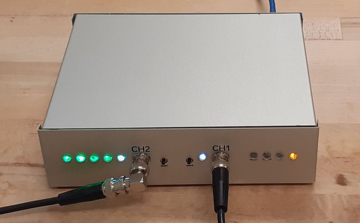
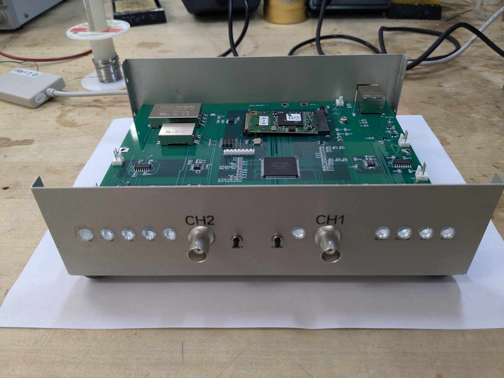
[01-MAR-25] The Function Generator (A3050) is a Power-over-Ethernet (PoE), two-channel, programmable signal generator. The latest version provides sinusoidal output from 1 mHz to 2 MHz with an output dynamic range of ±10 V for high-impedance loads and ±5 V for 50-Ω loads. We connect the generator to our local area network (LAN) with a PoE switch. It then acts as a TCPIP (Transmission Control Protocol and Internet Protocol) server with its own address and listening port. The function generator contains two signal sources, each of with its own 8-KByte waveform memory, 13-Bit waveform length, 32-Bit clock divisor, 8-Bit DAC (Digital to Analog Converter), variable low-pass filter, variable attenuator, power amplifier, and 50-Ω output.
To communicate with the function generator, we open a socket to its listening port. Once the socket is established, we read and write bytes to the socket using a binary messaging protocol. These messages perform simple actions such as writing to or reading from a location in the function generator's memory. When shipped, the A3050 is configured with address 10.0.0.37 and listens on port 90. We can change the address and listening port of the function generator by uploading a new TCPIP configuration to its non-volatile memory. We can return the default address and port by performing a reconfiguration reset.
Each function generator channel can be either enabled or disabled. When we disable a channel, which is the state they enter after reset of power-up, the white enabled light next to a channel's output socket will be turned off. The output voltage will be 0 V. When enabled, the white light turns on. The function generator reads the first location in the channel's waveform memory and uses the byte it reads to drive the channel's eight-bit output DAC. The function generator steps through the waveform memory, reading consecutive bytes and updating the output DAC, until it reaches the final point in the waveform, as dictated by the channel's thirteen-bit waveform length register. It returns to the first location and generates the waveform again. The frequency at which it increments its way through the waveform memory is called the update frequency. The update clock is generated by dividing the function generator's 40-MHz waveform clock by the update divisor. Each channel has its own thirty-two bit update divisor.
| Parameter | Specification |
|---|---|
| Output Range, High-Impedance Load | ±10 V |
| Output Range, 50-Ω Load | ±5 V |
| Waveform Length | 2-8192 points |
| Minimum Update Frequency | 9.3 mHz |
| Maximum Update Frequency | 20 MHz |
| Maximum Settling Time | 150 ns to 90% |
| Waveform Digital Range | 0-255 |
| Waverform Digital Precision | 8-bit |
| Waverform Frequency Precision | 0.01% |
| Digital Value for Zero Volts | 128±1 |
| Disabled Output Value | ±50 mV |
| Configurable Low-Pass Filter | 14 Hz to 13 MHz |
| Configurable Attenuatition | 0 dB to 30 dB |
The DAC output passes through a configrable low-pass filter, a configurable attenuator, an output amplifier, and a 3-W, 50-Ω resistor. The low-pass filter we configure by writing to a register. It provides low-pass corner frequencies of 14 Hz to 13 MHz. The purpose of the filters is to smooth out the sudden changes in output voltage that occur when the function generator updates its output by reading a new byte from the waveform memory. The attenuator we configure with another register. The attenuator provides attenuation of roughly 0 dB to 30 dB in steps of 5 dB or 10 dB. The purpose of the attenuator is to make it possible for the function generator to provide accurate small-amplitude signals despite the fact that, before attenuation, the smallest output voltage step is 40 mV into 50 Ω. To generate a 100-mVpp sine wave into 50 Ω, the generator first produces a 3.2-Vpp sine wave, and then attenuates by 30 dB to obtain the 100-mVpp.
We configure the function generator by writing to the waveform memory, setting the update divisor, filter register, attenuation register, and finally the waveform length. We set the waveform length last because the function generator is disabled so long as the waveform length is zero. As soon as we se the waveform length to some value other than zero, the function generator begins to update its output at the update frequency. The actual waveform length is equal to the value we write to the waveform length register plus one. So if we write a 1 to the waveform length register, we get a waveform of two points. A similar increment occurs with the update divisor. If we write 31 to the update divisor register, the function generator divides its 40-MHz waveform clock by 32 to obtain the update frequency. The minimum value of update divisor is 2, for which we set the divisor register to 1. Thus the highest update frequency is 20 MHz.
[21-FEB-25] The following versions of the Function Generator (A3050) are defined.
| Version | Range (High Z) |
Range (50 Ω) |
Minimum Frequency |
Corner Frequency |
Comment |
|---|---|---|---|---|---|
| A3050A | ±9.5 V | ±4.8 V | 2.2 μHz | 2 MHz | Prototype |
| A3050B | ±9.5 V | ±4.8 V | 2.2 μHz | 1 MHz | Discontinued |
| A3050C | ±10.0 V | ±5.0 V | 2.2 μHz | 2 MHz | Active |
For each version, we give the minimum square wave frequency, as dictated by the length of the update divisor in the generator's firmware, and the maximum frequency, as defined by a 1 dB drop in sinusoidal output amplitude compared to the low-frequency amplitude.
[02-MAR-25] The generator steps through its waveform memory at the update frequency. The update frequency is some integer fraction of the waveform clock. In the A3050, the waveform clock is 40 MHz. The highest update frequency available is 20 MHz and the lowest is 9.313 mHz. Let k be the number of points we cycle through in our waveform memory to generate the waveform. In the A3050, we can have k from 2 to 8192. Let r be the ratio of the waveform clock to the update clock frequencies. Let f_w be the waveform freqeuncy itself. If we encode one complete waveform in our k points, then the output frequency, f will be:
f = f_w × (1 / rk)
In this manner, we can generate waveforms of any integer fraction of f_w, but no other frequencies. With f_w = 40 MHz, we can generate 597.015 kHz and 588.235 kHz by dividing f_w by 67 and 68 respectively, but we cannot generate 590 kHz. In order to generate an arbitrary frequency to within ±0.01%, we must write more than one waveform to the waveform memory. Suppose we write m complete waveforms to the waveform memory, taking up the same k points. Now we have:
f = f_w × (m / rk)
To obtain 590 kHz, we must divide 40 MHz by 67.797, so we are looking for m, r, and k such that rk/m is as close as possible to 67.797. We also want to make sure we have a sufficient number of points in each complete waveform. The number of points per wave is n = k/m. For a sinusoid, let us suppose we want to have n ≥ 32. But we do not have to have an integer number of points per waveform. We could have ten waveforms expressed in 101 points, so that the number of points per wave is 10.1. This acceptance of a fractional number of points per waveform is what allows us to obtain ±0.01% frequency precision with our 8192-point waveform memory.
Our own algorithm for choosing r, k, and m is implemented in the LWDAQ_configure procedure of LWFG.tcl. We begin by calculating the approximate number of points we need to create one cycle of the waveform if we run the update clock at its highest frequency. If this number of points is greater than the length of the waveform memory, we increase the waveform clock divisor until one complete waveform fits in the waveform memory. On the other hand, if the number of points is less than 4000, we increase the number of cycles in the waveform until the number of points is between 4000 and 8192. We now have our divisor, number of points, and number of cycles, and we can generate the waveform points. The table below presents the result of this algorithm for a range of frequencies.
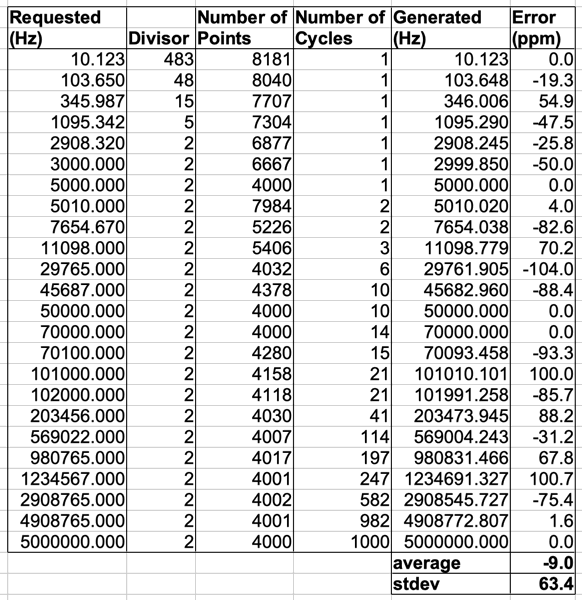
For any frequency above 2 kHz, we run the update clock at its fastest rate: 2 MHz. As the frequency increases above 5 kHz, we include more and more complete cycles in the waveform. The waveform always consists of somewhere between 4000 and 8192 points. The result is a generated frequency error of ±100 ppm = ±0.01%.
The generator's attenuators allow us to reduce the size of the DAC steps in our output waveform. Starting with the greatest attenuator setting, we see if the generator is capable of providing the requested output low and high levels with the attenuator enabled. If we request 100 mVpp with zero offset, we can engage the 29 dB attenuator and obtain the requested output with a 2.78 Vpp signal applied to the attenuator. If we cannot provide the output levels with the greatest attenuator, we consider the next greatest, and so on, so that we always engage the largest attenuator we can.
The generator's low-pass filters allow us to smooth out the DAC steps. Our rule for picking the low-pass filter is simple: we pick the lowest corner frequency we can, provided it is at least sixteen times higher than the frequency of the wave we are generating. In the case of sinusoidal sweeps, we pick the filter to suit the highest frequency of the sweep.
[22-FEB-25] On the back side of the function generator is an RJ-45 socket. Connect this socket to a PoE (Power over Ethernet) switch with a network cable. The switch must be an industry-standard PoE switch, such as the TL-SG1005P or GS305P. The cable can be shielded or unshielded, but it must be CAT-5+ to support 100 Mbps communication. When you first set up the function generator, press RESET and CONFIG on the front panel at the same time. Release the RESET button, but keep holding the CONFIG button for three seconds. The function generator will reset its TCPIP configuration to its factory default. Its IP address will be restored to 10.0.0.37 and it will start listening on port 90.
If you want to change the IP address or listening port number, you can open a socket to the function generator and use the config_read and config_write instructions download the existing TCPIP configuration file and upload a modified version of the string. You will find code demonstrating how to perform the read and write in the network interface section below. But we suggest you perform your first re-configuration with our Configurator Tool. Download our LWDAQ Software as a zip archive from our dowload page, or clone the its repository from GitHub. Follow the instructions in the Configurator section of the LWDAQ Manual to update the IP address and port number. If you plan to use the LWDAQ Software as your base for controlling the function generator, we recommend you leave the port number at the default value of 90.
Once you have the IP address and port set to your liking, the function generator is set up and ready to use. You can configure it right away with the The SCT_Check.tcl tool in the LWDAQ Tools/More menu, or you can open a socket to the function generator with your own code, and start to read and write to its control registers. Do not worry about damaging the function generator with any kind of read or write: no such damage is possible. You can always restore the functiong generator by performing another configuration reset.
When you open a socket to to the function generator, make sure the socket is configured for binary byte transfer, without any newline characters or UTF-8 encoding restrictions. Once open, use the function generator's messaging protocol to read and write to locations in the function generator's memory map. Use our memory map tables to find the locations you need to write to.
[01-MAR-25] The function generator is a TCPIP server with a reconfiguratble IP address and server port number. The TCPIP interface is managed by an RCM6700 embedded processor. The interface is an example of a LWDAQ Server. We communicate with this server using the LWDAQ-TCPIP message protocol.
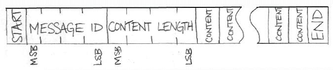
We open a socket to the function generator, using its IP address and listening port. We make sure the socket is configured for binary communication. We do not want the socket to restrict the communication to ASCII or UTF=8 characters. Nor do we want it to add a line break every time we flush our messages out of the socket. Once we have opened a socket, we can start to send messages. Each message has the format given above. The message begins with a start byte (0xA5). After that comes a four-byte message identifier and a four-byte content length. The content length can be zero, but if it is non-zero, we follow with that exact number of bytes. The message ends with an end byte (0x5A). We can transmit as many messages as we like. The code below shows how we can read the function generator's software version number.
When we have sent all the messages we want to send, we must take care how we terminate our communication. The protocol requires that we end our transmission with an EOT (End of Transmission, 0x04) byte. When the function generator receives this byte, it must immediately closes the socket, even if it has not finished executing the instructions it has received during the transmission. The last message we send must be a byte read, such as a version number read, and the client must wait until it receives the returned byte before writing the EOT byte and closing the socket for itself. The server will not execute the byte read until all the preceeding messages are processed, so we close the socket when the instructions are complete, but no sooner.
# Open a socket to the function generator at local address 192.168.1.14. We will
# connect to the standard LWDAQ server port, which is port 90.
set sock [socket 192.168.1.14 90]

# Configure the socket for binary data transfer. No newline characters will be
# added to data transmitted, nor will we wait for newline characters when we
# read.
fconfigure $sock -translation binary

# Compose the version read measage out of binary bytes, each of which we specify
# with an escape sequence. Write the message to the socket output buffer.
puts -nonewline $sock "\xA5\x00\x00\x00\x00\x00\x00\x00\x00\x5A"

# Transmit the message by flushing the output buffer.
flush $sock

# Read fourteen bytes from the socket, which will be the prefix byte, four
# message identifier bytes, four content length bytes, four software version
# bytes, and a suffix byte.
set message [read $sock 14]

# Scan these bytes for the prefix, identifier, length, version, and suffix.
# Write these values to the terminal.
binary scan $message H2IIIH2 prefix id len version suffix
puts "$prefix $id $len $version $suffix"

# Send the end of transmission byte to the server: we want it to close the
# socket right away.
puts -nonewline $sock "\x04"

# Close our side of the socket.
close $sock
The messages serve functions such as byte_write, stream_write, and version_read, each of which has its own numerical identifier. For a definitive presentation of the message types and their formats, we refer you to the messaging protocol specification. We summarize the message identifiers, names, and functionas in the table below.
| Message Identifier |
Name | Function |
| 0 | version_read | read relay software version |
| 1 | byte_read | read from controller location and return result |
| 2 | byte_write | write to controller location |
| 3 | stream_read | read repeatedly from controller location |
| 4 | data_return | message contains block of data |
| 5 | byte_poll | poll a controller byte until it equals specified value |
| 6 | login | send password to relay to attain higher access privilege |
| 7 | config_read | read relay configuration file |
| 8 | config_write | re-write relay configuration file |
| 9 | mac_read | read relay MAC address |
| 10 | stream_delete | write repeatedly to controller location |
| 11 | echo | receive and return the message contents |
| 12 | stream_write | write a block of data to a controller location |
| 13 | reboot | reboot the relay |
In the Tcl code below, we arrange to sets the attenuator register for channel number two (CH2) to 0x0F, which provides maximum attenuation of the raw signal before output.
# Open a socket to the function generator.
set sock [socket 192.168.1.14 90]
fconfigure $sock -translation binary

# Four byte writes to the data address locations set the data address to
# 0x00008017, which is the data address location of the CH2 attenuator register.
puts -nonewline $sock "\xA5\x00\x00\x00\x02\x00\x00\x00\x05\x00\x00\x00\x18\x00\x5A"
puts -nonewline $sock "\xA5\x00\x00\x00\x02\x00\x00\x00\x05\x00\x00\x00\x19\x00\x5A"
puts -nonewline $sock "\xA5\x00\x00\x00\x02\x00\x00\x00\x05\x00\x00\x00\x1A\x80\x5A"
puts -nonewline $sock "\xA5\x00\x00\x00\x02\x00\x00\x00\x05\x00\x00\x00\x1B\x17\x5A"

# A single byte write to the data portal sets the attenuator.
puts -nonewline $sock "\xA5\x00\x00\x00\x02\x00\x00\x00\x05\x00\x00\x00\x3F\x0F\x5A"

# Transmit a software version read and wait for reply. When we receive the reply, we
# send the EOT byte and close the socket.
puts -nonewline $sock "\xA5\x00\x00\x00\x00\x00\x00\x00\x00\x5A"
flush $sock
set message [read $sock 14]
puts -nonewline $sock "\x04"
close $sock
We read out the function generator's TCPIP configuration with the config_read job, which we illustrate below. We do not know how long the configuration file will be until we receive the data_return message. The content length in the data_return message will tell us how many bytes we should read from the socket to get the entire configuration file, but not a byte more.
# Open a socket to the function generator.
set sock [socket 192.168.1.14 90]
fconfigure $sock -translation binary

# Transmit a configuration read instruction.
puts -nonewline $sock "\xA5\x00\x00\x00\x07\x00\x00\x00\x00\x5A"
flush $sock

# Read the data return message header. The header consists of the prefix byte,
# four message identifier bytes, and four content length bytes.
set header [read $sock 9]

# Scan the header for the prefix, identifier, and length. Write these values to
# the terminal. The prefix should be 0xA5, the id should be 4, and the length
# should be 200-300 characters.
binary scan $header H2II prefix id len
puts "$prefix $id $len"

# Read len bytes from the socket, this being the configuration file. Because the
# configuration file is an ASCII document, we can print it right to the terminal.
set config [read $sock $len]
puts $config

# Now close the socket by sending the EOT character.
puts -nonewline $sock "\x04"
close $sock
In our case, what we see in the terminal is as follows.
lwdaq_relay_configuration:
subnet_mask: 255.255.255.0
ip_port: 90
configuration_time: 20250221133900
password: LWDAQ
operator: Kevan
gateway_addr: 192.168.1.1
tcp_timeout: 0
security_level: 0
driver_id: A3050_3353
ip_addr: 192.168.1.14
The reason this particular function generator is called the "A3050_3353" is because the last four digits of its MAC address is "3353". We can read out the MAC address of the function generator with the mac_read instruction. Suppose we want to change the IP address of the function generator to 192.168.1.61, and enable the TCP timeout, so that idle connections to the function generator will be closed automatically after ten seconds. We can achieve our objective with the following code.
# Open a socket to the function generator.
set sock [socket 192.168.1.14 90]
fconfigure $sock -translation binary

# Compose the new configuration file and print to the terminal.
set config "lwdaq_relay_configuration:
subnet_mask: 255.255.255.0
ip_port: 90
configuration_time: [clock format [clock seconds] -format "%Y%m%d%H%M%S"]
password: LWDAQ
operator: Kevan
gateway_addr: 192.168.1.1
tcp_timeout: 10
security_level: 0
driver_id: A3050_3353
ip_addr: 192.168.1.61"
puts $config

# Compose our message with the help of the big-endian four-byte integer format code "I".
# After we compose the entire message, we flush the socket.
set message "\xA5\x00\x00\x00\x08"
append message [binary format I [string length $config]]
append message $config
append message "\x5A"
puts -nonewline $sock $message

# Transmit a software version read, flush the socket and wait for reply. When we
# receive the reply, we sent the EOT byte and close the socket.
puts -nonewline $sock "\xA5\x00\x00\x00\x00\x00\x00\x00\x00\x5A"
flush $sock
set message [read $sock 14]
puts -nonewline $sock "\x04"
close $sock
The above code re-writes the EEPROM file that contains the TCPIP configuration. But this file is read only after reset or power-up, so we must now re-boot the function generator's TCPIP interface, which we can do with the reboot command. If you want to see exactly how the function generator handles incoming connections and messages, take a look at its LWDAQ server source code, C2037E15.c.
To configure the waveform memory, and so define a waveform, we use the stream_write message. The code below configures the channel two to produce a 625-kHz sinusoid of 10-Vpp into a 50-Ω load using 32 output points. The low-pass filter we set to 3.1 MHz and the attenuation to 0 dB.
# We define a full-scale sinusoid with thirty-two points ranging 0 to 255.
set values "128 152 176 198 218 234 245 253 255 253 245 234 218 198 176 152 \
	128 103 79 57 37 21 10 2 0 2 10 21 37 57 79 103"

# Open a socket to the function generator.
set sock [socket 192.168.1.14 90]
fconfigure $sock -translation binary

# Set up a stream write to the data space. Our target is the channel-two waveform memory,
# which starts at address 0x00004000.
puts -nonewline $sock "\xA5\x00\x00\x00\x02\x00\x00\x00\x05\x00\x00\x00\x18\x00\x5A"
puts -nonewline $sock "\xA5\x00\x00\x00\x02\x00\x00\x00\x05\x00\x00\x00\x19\x00\x5A"
puts -nonewline $sock "\xA5\x00\x00\x00\x02\x00\x00\x00\x05\x00\x00\x00\x1A\x40\x5A"
puts -nonewline $sock "\xA5\x00\x00\x00\x02\x00\x00\x00\x05\x00\x00\x00\x1B\x00\x5A"

# Now we peform the stream write to the data portal. The message identifier is twelve, the
# length is the number of values plus four for the control address of the stream write.
# The contents of the message are the data portal address, which is sixty-three, and the
# binary values defined by our values string.
set message "\xA5\x00\x00\x00\x0C"
append message [binary format I [expr [llength $values] + 4]]
append message "\x00\x00\x00\x3F"
append message [binary format c* $values]
append message "\x5A"
puts -nonewline $sock $message

# Four byte writes to the data address locations set the data address to point
# to the configuration registers of channel two, which start at 0x00008010.
puts -nonewline $sock "\xA5\x00\x00\x00\x02\x00\x00\x00\x05\x00\x00\x00\x18\x00\x5A"
puts -nonewline $sock "\xA5\x00\x00\x00\x02\x00\x00\x00\x05\x00\x00\x00\x19\x00\x5A"
puts -nonewline $sock "\xA5\x00\x00\x00\x02\x00\x00\x00\x05\x00\x00\x00\x1A\x80\x5A"
puts -nonewline $sock "\xA5\x00\x00\x00\x02\x00\x00\x00\x05\x00\x00\x00\x1B\x10\x5A"

# There are eight registers to set, but they are all consecutive in the data
# space, so we can write repeatedly to the data portal and the function
# generator will increment our data address automatically between writes. We
# write 0x00000001 to the divisor, 0x001F to the waveform length, which will
# enable the output, and finally we set the filter to 3.1 MHz and the attenuator
# to minimum.
puts -nonewline $sock "\xA5\x00\x00\x00\x02\x00\x00\x00\x05\x00\x00\x00\x3F\x00\x5A"
puts -nonewline $sock "\xA5\x00\x00\x00\x02\x00\x00\x00\x05\x00\x00\x00\x3F\x00\x5A"
puts -nonewline $sock "\xA5\x00\x00\x00\x02\x00\x00\x00\x05\x00\x00\x00\x3F\x00\x5A"
puts -nonewline $sock "\xA5\x00\x00\x00\x02\x00\x00\x00\x05\x00\x00\x00\x3F\x01\x5A"
puts -nonewline $sock "\xA5\x00\x00\x00\x02\x00\x00\x00\x05\x00\x00\x00\x3F\x00\x5A"
puts -nonewline $sock "\xA5\x00\x00\x00\x02\x00\x00\x00\x05\x00\x00\x00\x3F\x1F\x5A"
puts -nonewline $sock "\xA5\x00\x00\x00\x02\x00\x00\x00\x05\x00\x00\x00\x3F\x11\x5A"
puts -nonewline $sock "\xA5\x00\x00\x00\x02\x00\x00\x00\x05\x00\x00\x00\x3F\x00\x5A"

# Transmit a software version read, flush the socket and wait for reply. When we
# receive the reply, we sent the EOT byte and close the socket.
puts -nonewline $sock "\xA5\x00\x00\x00\x00\x00\x00\x00\x00\x5A"
flush $sock
set message [read $sock 14]
puts -nonewline $sock "\x04"
close $sock
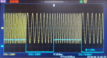
We modify the above code in the following way to create a rougher version of the same sinusoid on channel one. We stream write to the channel-one waveform memory at 0x00000000 and we write 0x01 to the channel-one filter register to select the 13-MHz low-pass filter.
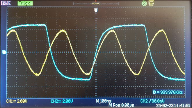
In the traces above, we see the smoothing of the 3.1-MHz filter in the blue sinusoid, and also the slight decrease in amplitude that results from this filter.
[06-MAR-25] The A3050 presents itself as a 64-byte (6-bit) control space and a 4-GByte (32-bit) data space. The control space is accessible throught the LWDAQ-TCPIP byte_read and byte_write instructions. The control space is restricted to 64 locations because the interface between the embedded computer that runs the TCPIP stack and the logic that produces the waveforms provides an address bus of only six bits. In order to provide access to the waveform memory, we use four locations in the control space to hold a 32-bit data address that points to a location in the data space. Another location in control space, which we call the data portal, permits reading and writing from the location pointed to by the data address. The byte_write instruction specifies the control address and a byte to write. The byte_read instruction specifies a control address to read, then returns the byte read from that control address.
| Control Space Address (Hex) |
Control Address (Decimal) |
Contents |
|---|---|---|
| 00 | 0 | Hardware identifier |
| 12 | 18 | Hardware version |
| 13 | 19 | Firmware version |
| 18 | 24 | Data Address, Byte 3 |
| 19 | 25 | Data Address, Byte 2 |
| 1A | 26 | Data Address, Byte 1 |
| 1B | 27 | Data Address, Byte 0 |
| 3F | 63 | Data portal |
All registers necessary for controlling the function generator are located in the data space. To gain access to the function generator's data space, we write the 32-bit data space address to the four data address registers using four byte_write instructions. We can then write to or read from the specified data address location using a byte_write or byte_read to the data portal address. After any byte_write or byte_read the data address increments automatically, so that we can immediately write to or read from the next location in the data space with another byte_write or byte_read. If we want to write a block of data to the data space, however, we can use the stream_write instruction, which takes as its content a block of bytes to be written consecutively to the data portal.
| Data Address (Hex) |
Data Address (Decimal) |
Contents |
|---|---|---|
| 0000..1FFF | 0..8191 | Waveform Memory, Channel 1 |
| 4000..5FFF | 16384..24575 | Waveform Memory, Channel 2 |
| 8000 | 32768 | Divisor, Channel 1, Byte 3 |
| 8001 | 32769 | Divisor, Channel 1, Byte 2 |
| 8002 | 32770 | Divisor, Channel 1, Byte 1 |
| 8003 | 32771 | Divisor, Channel 1, Byte 0 |
| 8004 | 32772 | Waveform Length, Channel 1, Byte 1 |
| 8005 | 32773 | Waveform Length, Channel 1, Byte 0 |
| 8006 | 32774 | Filter Control Register, Channel 1 |
| 8007 | 32775 | Attenuator Control Register, Channel 1 |
| 8010 | 32784 | Divisor, Channel 2, Byte 3 |
| 8011 | 32785 | Divisor, Channel 2, Byte 2 |
| 8012 | 32786 | Divisor, Channel 2, Byte 1 |
| 8013 | 32787 | Divisor, Channel 2, Byte 0 |
| 8014 | 32788 | Waveform Length, Channel 2, Byte 1 |
| 8015 | 32789 | Waveform Length, Channel 2, Byte 0 |
| 8016 | 32790 | Filter Control Register, Channel 2 |
| 8017 | 32791 | Attenuator Control Register, Channel 2 |
The thirty-two bit value we write to the four divisor bytes must be one less than the divisor we wish to implement. If we write the value 3 (0x00000003) to the divisor, the waveform length will be 3 + 1 = 4. The same increment applies to the value we write to the waveform length bytes. If we write 31, the waveform length will be 31 + 1 = 32. If we write a zero (0x0000) to the waveform length, we disable the output.
Time constants specified by various binary, hexadecimal, and decimal values written to a filter control register are given below.
| Binary | Hex | Decimal | Resistance | Capacitance | Time Constant | Corner Frequency |
|---|---|---|---|---|---|---|
| 00000001 | 01 | 1 | 51 Ω | 250 pF | 12 ns | 13 MHz |
| 00010001 | 11 | 17 | 51 Ω | 1 nF | 51 ns | 3.1 MHz |
| 00010010 | 12 | 18 | 110 Ω | 1 nF | 110 ns | 1.4 MHz |
| 00010100 | 14 | 20 | 270 Ω | 1 nF | 270 ns | 590 kHz |
| 00011000 | 18 | 24 | 560 Ω | 1 nF | 560 ns | 280 kHz |
| 00100001 | 21 | 33 | 51 Ω | 22 nF | 1.12 μs | 142 kHz |
| 00100010 | 22 | 34 | 110 Ω | 22 nF | 2.42 μs | 66 kHz |
| 00100100 | 24 | 36 | 270 Ω | 22 nF | 5.94 μs | 27 kHz |
| 00101000 | 28 | 40 | 560 Ω | 22 nF | 12.3 μs | 13 kHz |
| 01000001 | 41 | 65 | 51 Ω | 500 nF | 25.5 μs | 6.2 kHz |
| 01000010 | 42 | 66 | 110 Ω | 500 nF | 55 μs | 2.9 kHz |
| 01000100 | 44 | 68 | 270 Ω | 500 nF | 135 μs | 1.2 kHz |
| 01001000 | 48 | 72 | 560 Ω | 500 nF | 280 μs | 570 Hz |
| 10000001 | 81 | 129 | 51 Ω | 20 μF | 1.0 ms | 160 Hz |
| 10000010 | 82 | 130 | 110 Ω | 20 μF | 2.2 ms | 72 Hz |
| 10000100 | 84 | 132 | 270 Ω | 20 μF | 5.4 ms | 29 Hz |
| 10001000 | 88 | 136 | 560 Ω | 20 μF | 11 ms | 14 Hz |
The attenuation registers allow us to generate a signal much larger than we need, then attenuate it just before output so as to reduce the quantization noise we see on the final output. The table below gives the attenuation values we obtain by measurement of our first five function generators.
| Binary | Hex | Decimal | Attenuation (V/V) | Attenuation (dB) |
|---|---|---|---|---|
| 0000 | 00 | 0 | 1.04 | −0.34 dB |
| 0001 | 01 | 1 | 0.320 | +9.9 dB |
| 0011 | 03 | 3 | 0.116 | +19 dB |
| 0111 | 07 | 7 | 0.0588 | +25 dB |
| 1111 | 0f | 15 | 0.0360 | +29 dB |
Upon reset, which we can invoke with the reset button or by unplugging and re-plugging the PoE cable, the registers return to the following values.
| Parameter | Reset Value | Effect |
|---|---|---|
| Output Value | 0x80 | Output Zero |
| Update Divisor Register | 0x00000000 | No Update |
| Waveform Length Register | 0x0000 | Channel Disabled |
| Filter Control Register | 0x01 | Highest Corner Frequency |
| Attenuation Control Register | 0x00 | Minimum Attenuation |
All of the above registers can be addressed through the data portal, which is in turn accessible through the function generator control space. We write the register address to the data address locations in the control space, then we write to the data portal to perform the write into data space. The byte_write instruction is good for setting individual registers, but it is inefficient for loading waveforms into the waveform memory. To upload a waveform, we should use the stream_write instruction.
[01-MAR-25] We illustrate how one might build an interface for the function generator by presenting the interface we have built in Tcl. This interface resides in our LWDAQ Software, which allows it to make use of routines that manage TCPIP sockets without causing our application to freeze. That is: our sockets are non-blocking so that we can move windows around and press buttons in our Tk user interface while our application is trying to configure the function generator. If the function generator should fail to respond, for example, the code we presented in the Network Interface section would cause our application to freeze. If you would like to try the LWDAQ interfae, we invite you to clone the LWDAQ Repository. You can run LWDAQ right away on Linux, MacOS, or Windows, by following the installation instructions in our LWDAQ Manual.
In the LWDAQ program, message transmission is performed by LWDAQ_transmit_message, which in turn calls the flexible and forgiving LWDAQ_socket_write. You will find the transmit message routine in Driver.tcl and the socket write routine in Utils.tcl. Here is a simplified version of the transmit routine, which uses only "puts" to write to the socket.
proc LWDAQ_transmit_message {sock id contents} {
	global LWDAQ_Driver
	set message [binary format H2II \
		$LWDAQ_Driver(lwdaq_prefix) \
		$id \
		[string length $contents] ]
	append message $contents
	append message [binary format H2 $LWDAQ_Driver(lwdaq_suffix)]
	puts -nonewline $sock $message
	return ""
}
Note that we have stored the prefix and suffix bytes in a global array, so we can avoid typing in their binary values in every one of our messaging routines. In the LWDAQ program, data message reception is performed by LWDAQ_receive_data. Here a simplified version of the message receive routine, from which we have removed the LWDAQ-specific socket routines and all error checking. We refer to constants that tell us the header and suffix length.
proc LWDAQ_receive_data {sock} {
	global LWDAQ_Driver

	binary scan [read $sock $LWDAQ_Driver(lwdaq_header_length)] \
		H2II prefix id content_length
	set contents [read $sock $content_length]
	set last_byte [read $sock $LWDAQ_Driver(lwdaq_suffix_length)]

	return $contents
}
The Driver.tcl file contains many more routines for communicating with LWDAQ servers, all of which use the transmit and receive routines given above. All these routines are listed and described in the LWDAQ Command Reference. We write to a byte in control space with LWDAQ_byte_write. We read with LWDAQ_byte_read. Writing to the data space is a two-step process. We first use LWDAQ_set_data_addr to write four bytes to the data address, which resides in the control space. We then use LWDAQ_stream_write to write a block of data to the data portal, which is a single byte in control space. In the commands below, we configure a function generator to produce a 10-kHz, 32-point sinusoid on channel two with minimum attenuation and highest filter frequency.
# Connect to the function generator at address $ip.
set sock [LWDAQ_socket_open $ip]

# Construct the full-scale sinusoidal wave consisting of thirty-two points.
set values "128 152 176 198 218 234 245 253 \
	255 253 245 234 218 198 176 152 \
	128 103 79 57 37 21 10 2 \
	0 2 10 21 37 57 79 103"

# Write the waveform to the channel-two waveform memory.
LWDAQ_set_data_addr $sock 16384
LWDAQ_stream_write $sock 63 [binary format c* $values]

# Set the channel-two waveform length register to one less than the waveform
# length.
LWDAQ_set_data_addr $sock 32788
LWDAQ_stream_write $sock 63 [binary format S 31]

# Set the channel-two update divisor to produce 320 kHz update from 40 MHz. We
# set the divisor to be one less than 40 MHz / 320 kHz.
LWDAQ_set_data_addr $sock 32784
LWDAQ_stream_write $sock 63 [binary format I 124]

# Set the channel-two filter register to the highest frequency.
LWDAQ_set_data_addr $sock 32790
LWDAQ_stream_write $sock 63 [binary format c 1]

# Set the attenuator configuration register to minimum attenuation.
LWDAQ_set_data_addr $sock 32791
LWDAQ_stream_write $sock 63 [binary format c 0]

# Wait for the controller to be done with configuration.
set id [LWDAQ_hardware_id $sock]
Our Long-Wire Function Generator (LWFG.tcl) package provides commands that configure the function generator with a single line of Tcl code. We load this package into LWDAQ with "package require LWFG". The main routines provided by LWFG are LWFG_configure and LWFG_sweep. The configure routine does everything necessary to set one of the function generator outputs to a sine, square, or triangle wave. The sweep routine configures the generator to produce a sinusoidal sweep.
LWFG_configure ip ch_num waveform frequency v_lo v_hi
Here, ip is the IP address of the function generator's TCPIP server. The LWFG routines assume that the function generator is listening on port 90. We have channels CH1 and CH2, which we identify with 1 and 2. The two voltages v_lo and v_hi are the voltages of the minimum and maximum points in the waveform respectively, assuming that the output is terminated with a high-impedance load, not a 50-Ω load. For the waveform we can specify "sine", "square", or "triangle". We do not specify the attenuator or filter settings, because the LWFG configure routine will select the attenuator and filter for us automatically to suit the waveform it uploads to the generator.
LWFG_sweep_sine ip ch_num f_lo f_hi v_lo v_hi t_len log
The sweep routine takes eight parameters: IP address, channel number, low frequency for the sweep, high frequency, low voltage for the sinusoid, high voltage for sinusoid, time for the entire sweep to complete, and a flag for logarithmic or linear frequency variation. As with the configure routine, the low and high voltages apply to the function generator output with a high-impedance load. The routine sets the filter function to suit the highest frequency in the sweep. The sweep generated by this routine is always low frequency to high frequency. Here is the code that generates the sweep, extracted from the LWFG package.
set values [list]
set period [expr 1.0*$num_pts]
set pi 3.141592654
for {set i 0} {$i < $num_pts} {incr i} {
  set phase [expr fmod($i,$period)/$period]
  if {$log} {
    lappend values [expr $dac_lo + \
      round(($dac_hi - $dac_lo) * 0.5 * \
        (1.0+sin(2*$pi*($f_lo*$t_len* \
          ((pow(($f_hi/$f_lo), ($phase)) - 1) \
            /(log($f_hi/$f_lo)))))))]
  } else {
    lappend values [expr $dac_lo + \
      round(($dac_hi - $dac_lo) * 0.5 * \
        (1.0+sin(2*$pi*$t_len*(($f_lo+ \
          (($f_hi-$f_lo)/2)*$phase)*$phase))))]
  }
}
Here is a specific example of the routine in use.
LWFG_sweep_sine 192.168.1.14 1 100 500 -10.0 +10.0 0.1 1
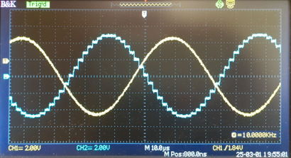
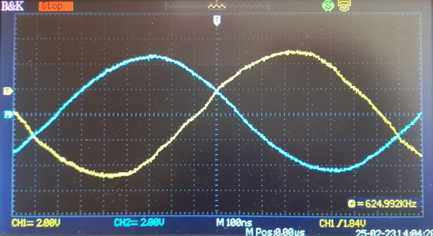
The above command creates a sweep from 100 Hz to 500 Hz with a logarithmic progression, full-scale, taking 100 ms. The sweep waveform occupies the entire channel-one waveform memory. It consists of 8192 eight-bit values that trace out the entire sweep waveform. You will find these values in Sweep_1.txt. The yellow trace below shows what the sweep looks like.
The SCT_Check.tcl tool in the LWDAQ Tools/More menu is an example of an application of the function generator to measure the frequency response of telemetry sensor amplifiers and record the frequency response as a table of numbers. It allows us to enter "sine", "square", "triangle", and "sweep" for the output waveform. Entry boxes specify frequencies in Hertz and peak-to-peak amplitude with 50-Ω termination.
[03-MAR-25] When we generate a sinusoid, we would like it to be a pure sinusoid. The Fourier series expansion of the ideal sinusoid is one peak at the fundamental frequency, and nothing more. Our calculation of the ideal points along our generated sinusoids is precise to ten significant figures, but we curtail this precision as soon as we write the values to our waveform memory, because the waveform memory accepts only values 0-255. The distortion of our sinusoid that is caused by rounding our voltages to the nearest value 0-255 is what we call quantization noise. Each time we update our output, the update occurs suddenly on the output of our converter. Our low-pass filters attempt to reduce these sudden steps, but they cannot do a perfect job without reducing the amplitude of our larger waveform.
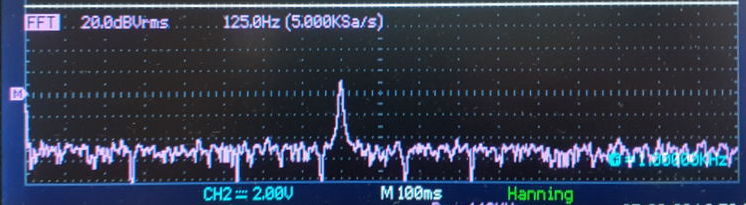
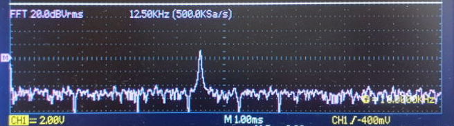
Given that our sinusoids are not going to be perfect, we might ask what kind of imperfections are most tolerable in a test fixture. In our experience, stochastic noise disrupts our measurements less than coherent noise. We therefore choose to set up our function generator so that its distortion appears randomised and stochastic rather than coherent. When we generate a 1.2-MHz sinusoid, we do so by writing 247 cycles of the waveform to our waveform memory. The converter quantization noise is not coherent with the waveform frequency because the steps do not occur in the same location of the sinusoid in each cycle written to the memory. The quantization noise amplitude is not reduced by this incoherence, but the quantization noise spectrum has no peaks.
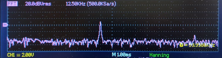
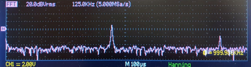
Once we get to 100 kHz, we start to see a peak in the spectrum at twice the fundamental frequency. Its power is 40 dB less than that of the fundamental, meaning its amplitude is 1% of the fundamental amplitude. At 1 MHz, the peak is 30 dB less powerful than the funamental, so its amplitude is 3% of the fundamental. The second harmonic is a result of the asymmetry of the output waveform. This asymmetry is visible in the 2-MHz sine wave shown in our Settling_Time image. In future versions of the function generator, we hope to find and eliminate the source of this asymmetry, so as to reduce the amplitude of the second harmonic.
[18-MAR-25] All our designs are free and open-sourcde, copyright Open Source Instruments Inc, under the GPL 3.0 license. This circuit was designed by Nathan Sayer, but it is based upon the design of the Function Generator (A3031) by Michael Bradshaw.
S3050C_1: Schematic for A3050C, Page 1.The function generator logic runs off an 80-MHz clock. It divides this 80 MHz by two to obtain its 40-MHz waveform clock, which it then divides further by a user-programmable update divisor to generate the update frequency. The bytes read from the waveform memory drive the eight-bit DACs directly. The DACs produce 0-3.3 V. A level shifter takes the DAC output and turns it into −1.65 to +1.65 V. Amplifiers convert this range into ±10 V. After the final amplifier, we have a 50-Ω 3-W resistor, which makes the outputs tolerant of continuous short-circuits.
The signal itself will be made up of at least two sample values, and all these values will be written to the waveform memory during waveform configuration. Our LWFG routines always uses at least half of the 8-KByte memory by repeating the waveform as many times as necessary. By allowing itself to repeat the waveform, we are able to generate frequencies with precision better than ±0.1%.
[21-NOV-24] To create the A3050C out of the A3050B, we load 270 Ω for the attenuator series resistors R86 and R91. We load divider resistors 100 Ω, 27 Ω, 10 Ω, and 3.3 Ω for both channels. We load 2.2 kΩ for R46 and R58 to increase the output amplitude.
[04-NOV-24] For a chronological account of the development and production of the A3050, see its Development page. That page provides an account of our work on discrete-component DC-DC converters, which we may deploy in later versions of the A3050, or in other LWDAQ systems of Form C.