[10-FEB-25] We propose to replace the RCM6700 deployed in the A3050 with a RPi 3B+, like the ones we use in the A3034C. When we try to use the GPIO lines directly as a parallel interface, we immediately encounter three problems. First, any time we generate a rising edge on a GPIO, we see a 100-ns HI pulse, 500-ns LO, and then the rising edge we want. Second, we cannot write to more than one GPIO at a time. Third, when we toggle a single GPIO as fast as we can, it goes at only 100 Hz.
raspi-gpio set 2 op dl
raspi-gpio set 2 op dh
There are two SPI interfaces on the GPIO connector. We enable one on a 3B+ and see it trying to run at 100 MHz. We are trying to figure out how to set the speed from the command line, or the /boot/config.txt file. We come across the pigs utility. This utility is installed on our 3B+.
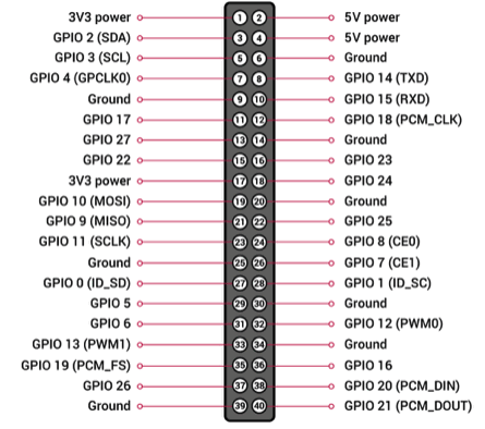
[11-FEB-25] We consult the RPi 40-Pin GPIO pinout, and the pinouts for RPi listed in the pigs manual, which we reproduce below.
                      MISO   MOSI   SCLK   CE0   CE1   CE2
           Main SPI      9     10     11     8     7     -
           Aux SPI      19     20     21    18    17    16
Here we have Master In Slave Out (MISO), Master Out Slave In (MOSI), Serial Clock (SCLK), and Chip Enable (CE). We can configure the SPI bus to have MISO default HI, and the CE lines can be positive-true or negative-true. We use the following lines to close any pre-existing Main SPI interface and send a single byte to MISO.
$ sudo pigpiod                                              # Start pigs daemon.
$ ps -e | grep pigpiod
 7247 ?        00:00:02 pigpiod
$ pigs spic 0                                                    # Close handle zero.
-25
ERROR: unknown handle
$ pigs spio 0 1000000 0                                          # Open Main SPI at 1MHz.
0                                                                # The handle is 0.
$ pigs spiw 0 0xAA                                               # Transmits 1 byte.
$ pigs spiw 0 0xAA 0xAA 0xAA 0xAA 0xFF 0x00 0xFF 0x00 0x33 0x33  # Transmits 10 bytes.
$ pigs spic 0                                                    # Close handle zero.
$ pigs spiw 0 0xAA                                               # Write to handle zero.
-25
ERROR: unknown handle
We make sure the pigs daemon is running. We close any preexisting connection to the Main SPI, which is SPI number zero. We open a new connection to SPI zero, setting the SPI clock rate to 1 MHz and using default flags. We hook our oscilloscope up to SCLK, MOSI, and CE0.

We increase the clock frequency to 20 MHz and try again. The clock frequency we observe is indeed 20 MHz. The signals show noise, but no significant overshoot. We see that the chip select line goes low 700 ns before the byte transmission.
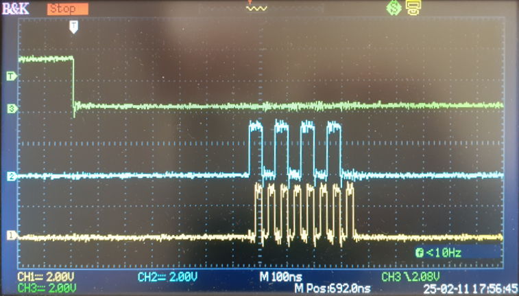
We transmit ten bytes and the entire transmission takes 6.5 μs, allowing for the delay after CS asserted and another 1 μs after CS unasserted. We transmit 40 bytes in 18 μs. It looks like we can achieve 2 MByte/s with this interface.
[17-FEB-25] We power up an RPi 3B+ from 5V through an ammeter. Current consumption during the first minute is 50-470 mA with a median of around 250 mA. After boot, we see 230-270 mA when the RPi is idle.
[18-MAR-25] We start the detailed design of this new PoE function generator with LWDAQ server. We will mount a Raspberry Pi 3B+ onto the board and connect to it using a short 40-way ribbon cable and a short 4-way ribbon cable, in the same way we do in our A3034C circuit.
[19-MAR-25] We examine our existing S3050X converter design. We have been running the 5-V version for the past six months with a 5-Ω load. We just turned it off and put it away. The design uses the LT8306 no-opto flyback regulator. But there are a few problems we see with the design. The peak current in the switch is 10 A, but the transformer primary saturates at 1.3 A. There is no snubber ciruit to damp the ringing of the transformer, and we would like to minimize noise in our function generator. The circuit is complicated by an external switch, when we could be using the LT8304 regulator with internal switch. The transformer is too tall to fit in a standard module. We could be using something smaller and higher-current from Coilcraft.
We consider what is available in surface-mount, commercial off-the-shelf isolating DC-DC converters. We have been using the CC-E 48-V converters for five years with no failures. The dual-output versions are more difficult to find. We propose to use single-output only. We need to supply the RPi with up to 2.5 W, and we propose to obtain most of our 3.3-V power from the RPi's on-board converter. We suggest the CC6-4805SR-E, 6-W, 5-V output, $15 in QTY 50. For our function generator power amplifiers, we suggest two of the CC3-4812SR-E, 3-W, 12-V output, $10 in QTY 50. Our total converter cost is $35. With two 3-W, 12-V converters we can supply 250 mA from ±12 V. If we terminate two 10-V outputs with 50 Ω, we will draw 200 mA maximum. If we short one output and leave the other open circuit, we will draw up to 200 mA. If we short both outputs, the converter will shut down.
We look at converters in SIP-8 packages, 0.1" pitch, with between 5 and 7 pins loaded. We search for 3-W, 48-V input, single 12-V output and find 35 in stock at DigiKey, including RS3-4812S, MD348S-12CRW, AM3G-4812SEZ, SPBW03G-12, all with the same pinout. Dual-output converters in the SIP-8 also have a standard pinout. These converters are buit on their own circuit board with pins on one side, encapsulated in epoxy. The Traco Power TMR 12-4822WI is a 12-W, 48-V input, ±12-V output converter with a couple of extra case mounting pins, which we could cut off, and comes in a metal can, but otherwise standard pinout. The Cincon EC4SAW-48D12HN is a 6-W, 48-V input, ±12-V output converter for $14. Both claim >85% efficiency. The MeanWell SPBW06G-05 is a 6-W, 48-V input, 5-V output converter for $11. We resolve to place two SIP-8 converters on our board with P1206, 10-μF, 100-V input capacitors, and 10-μH, P0805, EMI blocking inductor.
[21-MAR-25] The original A3031 and subsequent A3050 function generators used the LT1206 ($11) high-current op-amp for both amplification and final power output. We propose to use one LM6172 ($3) dual op-amp for amplification and one LMH6321 ($3) for buffering. The first op-amp will take 0-3.0 V and turn it into ±5 V. The variable filter comes next, then another op-amp to turn ±5 V into ±10 V. Now comes the variable attenuator, and after the attenuator is the buffer and a2.4-W, 50-Ω output resistor, like the RCP1206W50R0GEB. The original circuits used the DG411DY analog switches to select resistors and capacitors for the filters and attenuators. These have channel resistance 25 Ω and channel-on capacitance 35 pF. Together, these give us a time constant of 0.9 ns, which is far less than the target 50-ns rise time of our new generator. Vishay Siliconix no longer makes the DG411DY, but other companies do. We will switch to the DG412DY, in which the switches close with a logic HI rather than a logic LO.
We will derive our main logic power from the RPi's converter, but we will derive the DAC digital output power supply from our own 5V0 using one TLV71330 3.0-V 1%-accurate regulator for each DAC. Our DAC output will be 0.0-3.0 V instead of the previous 0.0-3.3 V. We will route the eight DAC outputs of each channel through its own dedicated I/O bank on the logic chip. For our incoming PoE power switch, we will re-use the A3034C power receiver.
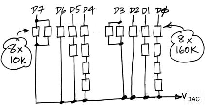
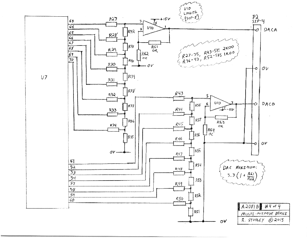
In the earlier circuits, we used two resistor values in parallel and series combinations to allow us to obtain precise factors of two from one bit to the next. We call this the eighteen-resistor DAC. We could try 0.1% resistors in values 10, 20, 40.2, 80.6, 160, 316, 642, and 1200 kΩ. We will have a 0.5% error in the third resistor, which is 0.1% of full range, or one quarter of a full step. Or we could use 4.87, 9.76, 19.6, 39.2, 78.7, 158, 316, 634 kΩ. This is the eight-resistor DAC. Another option is the sixteen-resistor ladder, as demonstrated by Richard Studley in his A2081 circuit. We have sixteen resistors of two values. We could use 10 kΩ and 20 kΩ. Output resistance is 10 kΩ. The two-value DAC circuits are cheaper to build, because they reduce the number of reels the assembly house must load onto their machine. The sixteen-resistor ladder requires that each output be able to drive a load of 3 kΩ or so. If we are going to increase current drive to the network, we must increase curren driver on all eight bits. But the eighteen-resistor network requires peak current only from the top bit, allowing us to provide 24 mA drive for the top bit, 8 mA for the second bit, and 4 mA for the rest. We will stick with the eighteen-resistor DAC.
[23-MAR-25] Our DAC output will have 256 states spanning 0.0-3.0 V. We use one half of an LM6172 to shift and amplity the DAC output so it spans ±5 V. We use the circuit shown below.
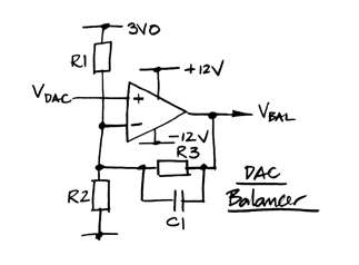
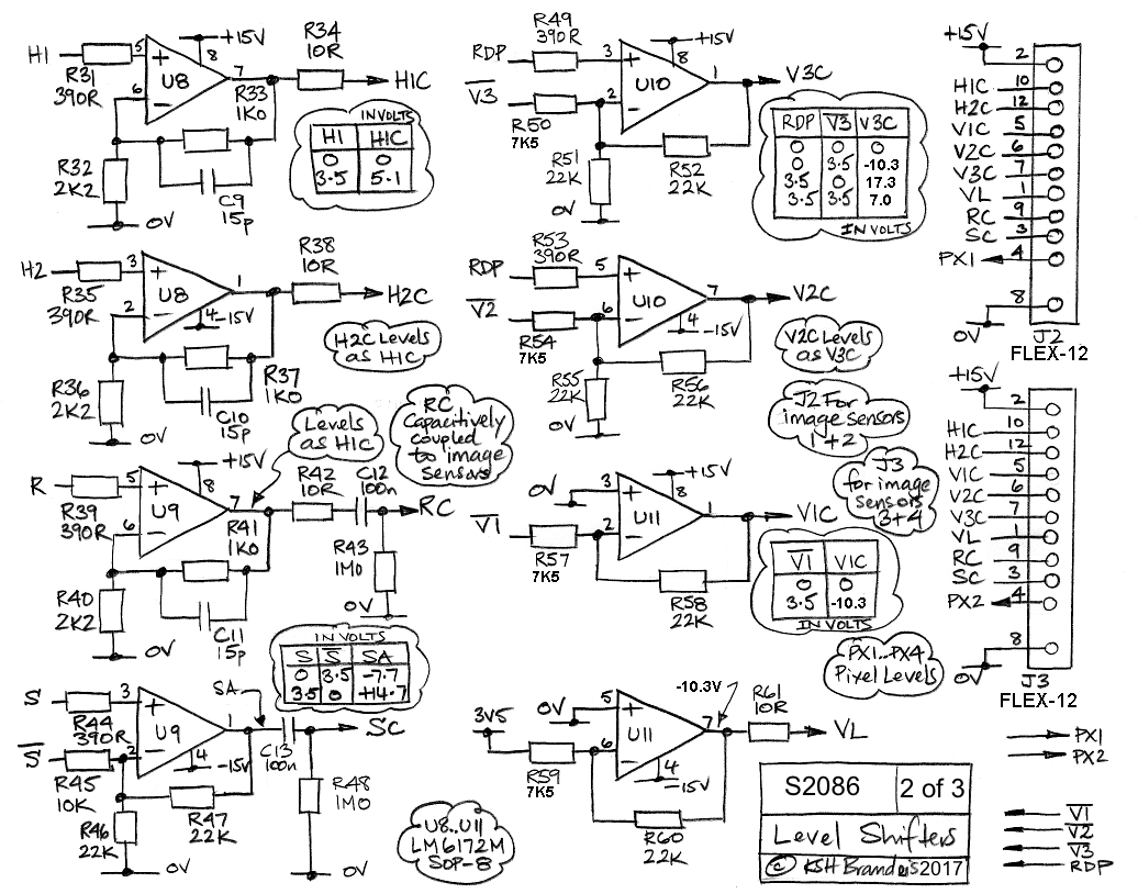
For the derivation that allows us to choose values for R1, R2, and R3, see DAC_Balancer_Eq. Example values that give a perfect result are R1 = 1.0 kΩ, R2 = 2.5 kΩ, and R3 = 1.7 kΩ. Other combinations are given in our DAC_Balancer_R table. Standard 1% values we can use are R1 = 1.00 kΩ, R2 = 2.49 kΩ, and R3 = 1.69 kΩ. We might add C1 = 15 pF to remove overshoot, as we do in the S2086 level-shifters.
The output from the DAC Balancer passes through the variable filter. The variable filter uses analog switches, let us assume they are DG412DY with 9-pF off capacitance and 35-pF on capacitance. Both these act as capacitance to ground from the drain or source or channel when the switch is off (open) or on (closed). To minimize the effects of these capacitances, we drive the resistor switches directly with our DAC Balancer, and we connect the capacitor switches directly to 0V.
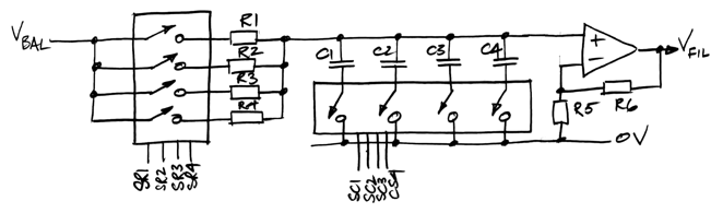
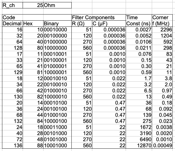
We must add to the resistor values the 25-Ω channel resistance of the switches. Following the pattern we used in the A3050, but accounting for the 25 Ω, and using standard values, we like R1 = 51 Ω, R2 = 120 Ω, R3 = 270 Ω, and R4 = 560 Ω. For the capacitors, we can try C1 = 1.0 nF, C2 = 22 nF, C3 = 470 nF, and C4 = 22 μF. These values produce the following time constants and corner frequencies.
[24-MAR-25] We devise a new variable attenuator circuit, consisting of a ladder of resistors. We have the analog switches connecting directly to ground. Let us assume the DG412DY as our switch. The on-state channel capacitance of 35 pF is charged and discharged by their on-state channel resistance of 25 Ω when the shunt resistor is connected to ground. Their off-state drain capacitance of 9 pF will be charged by the shunt resistors. Rise-time from these capacitances combined should be no more than 10 ns.
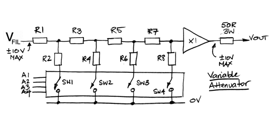
With the help of a Toolmaker script, we select suitable values of the shunt resistors. We fix the series resistors at 470 Ω and vary the others from 45 Ω to 1000 Ω in a brute force search for the shunt values that give us the most even progression of logarithmic attenuation.
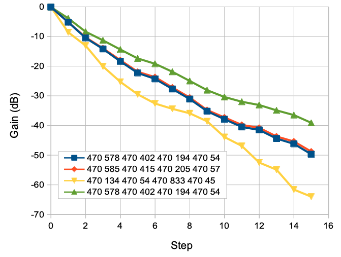
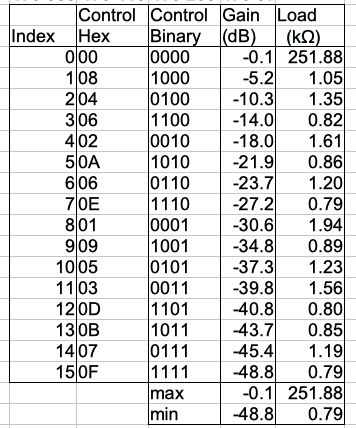
These networks present a load of around 1 kΩ for most steps, but reaching a minimum of 800 Ω for the highest attenuation. Our LM6172 op-amp can drive ±10 V into 1 kΩ from a ±12 V power supply. In implementing the network, we will choose resistor values that, when added to the 25-Ω on channel resistance of the DG412DY shunt switches, will give a close match to our ideal values. The result is a network that provides sixteen steps of roughly 4 dB each, so that we have attenuation 0 dB to 50 dB. The resistors that give the orange plot are R1 = R3 = R5 = R7 = 470 Ω, R1 = 560 Ω, R4 = 390 Ω, R6 = 180 Ω, and R8 = 22 Ω. The expected values for the attenuation are given in the table below.
[29-MAR-25] Finish all four pages of the A3052AV1 schematic.