 Telemetry Control Box (TCB)
© 2022-2024, Kevan Hashemi,
Open Source Instruments Inc.© 2022-2023, Nathan Sayer, Open Source Instruments Inc.
| 2022 | 2023 | 2024 |
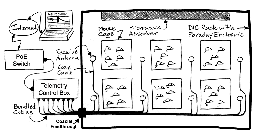
[24-APR-24] The Telemetry Control Box (TCB) is a telemetry receiver for devices such as our Subcutaneous Transmitters (SCT), Implantable Inertial Sensors (IIS), or Implantable Stimulator-Transponders (IST). The TCB-A16 provides sixteen antenna inputs, to which we can connect up to sixteen coaxial antennas, such as the Loop Antenna (A3015C). Each antenna input is equipped with its own dedicated receiver and power meter. The telemetry messages we record with a TCB contain not only the telemetry channel number and sample value, but also the identity of the top antenna, which is the antenna at which the message presented the greatest microwave power, and the top power, which is a logarithmic measure of the microwave power at the top antenna. The top antenna is almost always the antenna closest to the animal, so the to TCB's top antenna measurement allows us to monitor the location of animals in mazes and other complex environments. The TCB-B16 provides all the functionality of the TCB-A16, but in addition allows us to use the sixteen antennas as command transmitters, and provides four programmable, high-speed, digital communication lines. The command transmission allows us to use the TCB-B16 to control Implantable Stimulator-Transponders (ISTs). The digital communication lines allow the TCB-B16 to receive timing signals and transmit telemetry information to external devices.


The TCB requires only one network cable for communication and power, an industry-standard Power over Ethernet (PoE) connection. We supply the TCB with an Ethernet jumper cable so we can connect it to a PoE switch, and we sell high-reliability, fanless, PoE switches of various sizes for use with the TCB and our other PoE devices. When you order a TCB-A16, you can order up to sixteen Loop Antennas (A3015C) to go with it, depending upon how many you need to deploy in your telemetry system.

The TCB-A16 replaces the Octal Data Receiver (A3027E, ODR). The TCB-A16 provides sixteen antenna inputs, the ODR provided eight. Unlike the ODR, the TCB-A16 does not require a LWDAQ Driver (A2071E). The TCB-A16 provides a top antenna measurment, the ODR did not.
The following versions of the Telemetry Control Box (A3042, TCB) are defined.
| Version | Dimensions | Comment |
|---|---|---|
| TCB-A16 | 55 cm × 35 cm × 12 cm | 16-way receiver, location monitor. |
| TCB-B16 | 55 cm × 35 cm × 12 cm | 16-way receiver, location monitor, command transmitter, digital I/O. |
The TCB-A16 went into production in January 2023. We expect the TCB-B16 to be available by January 2025. The TCB-B16 provides command transmission through all sixteen antennas for controlling Implantable Stimulator-Transponders (ISTs). The TCB-B16 popluates the four holes X1-X4 on the back wall with four more BNC sockets. These will provide programmable, high-speed, digital input-output for experiments in which external stimuli need to be controlled in a manner synchronous with the telemetry signals, and in which synchronizing signals need to be embedded in the telemetry recording.
[23-SEP-23] The TCB obtains all its power and communication through a single Power-over-Ethernet (PoE) socket. The TCB system consists of the TCB, a PoE switch, coaxial cables, feedthroughs, and Faraday enclosures. In the paragraphs below, we provide detailed instruction on setting up the TCB for communication with your computer, but ultimately refer you to the SCT setup instructions once that communication is established.
Power Up PoE Switch: Connect power to your PoE switch. If you are not in the United States, you will need a computer power cable to connect to your local type of wall power socket, but you can be assured that the power adaptor will operate with any AC voltage 100-250 V, 50-60 Hz. Lights should illuminate on the PoE switch.
Connect TCB to PoE: Use a network cable to connect the TCB to the PoE switch. This cable can shielded or unshielded, and it can be up to ten meters long. Lights should illuminate on the TCB.
Install Software: Download and install the latest version of the LWDAQ software from here, following these installation instructions.
Connect Computer to PoE: Connect your data acquisition computer to the switch. Configure your computer to use its wired Ethernet interface with subnet 10.0.0.0 and IP address 10.0.0.20. The TCB ships with an IP address 10.0.0.x, where x is given by the last two or three digits of the serial number on the back of the TCB enclosure. The table below gives examples of serial numbers and their addresses.
| Serial Number | Address |
|---|---|
| Y61061 | 10.0.0.61 |
| Y61163 | 10.0.0.163 |
| P0148 | 10.0.0.148 |
| C0089 | 10.0.0.89 |
| Y70105 | 10.0.0.105 |
You should see a link light beside the sockets you have used on the PoE switch for your computer and your TCB. Launch the LWDAQ software and try to contact the TCB using the Configurator Tool, as described here. Don't proceed until you can contact the TCB and read its EEPROM.

Continue with Telemetry Setup: Connect antennas, set up software, and test out sample transmitters with the help of our Subcutaneous Transmitter (SCT) setup instructions, which you will find here.
In the Neuroplayer, if you can use the Neurotracker to see which antenna is receiving the most power from each of your transmitters, which is the TCB's measurement of animal location.
[08-FEB-24] We make the TCB-A16 by taking an Animal Location Tracker (ALT) Base Board (A3038BB-D2), putting it in a box, populating it with ALT Detector Modules (A3038DM-B2), connecting the detector modules to BNC sockets a Sixteen-Way Filtering Feedthrough (A3042FF-A) on the back wall of the box, connecting a Display Panel (A3042DP-A) to the base board, and fastening the display panel to the front of the box. We connect the ALT's RJ-45 socket to an RJ-45 feedthrough on the back wall of the box.

The TCB-B16 is identical to the TCB-A16 except its antenna connections pass through a Sixteen-Way Transmitting Feedthrough (A3042TF) equipped with sixteen Transmitter Modules (A3042TM). These additional circuits provide command transmission for Implantable Stimulator-Transponders (ISTs) as well as programmable, high-speed, digital input-output on the X1-X4 BNC sockets on the back wall.
| Version | Comments |
|---|---|
| A3038BB-D2 | ALT Base Board, no detector coils, re-programmed with P3042BB. |
| A3038DM-C2 | ALT Detector Module, unshielded, firmware P3038DM. |
| A3038DM-D3 | ALT Detector Module, shielded, firmware P3038DM. |
| A3042DP-A1 | Display panel with lights and switches, firmware P3042DP. |
| A3042SF-A1 | Sixteen-Way Straight Feedthrough. |
| A3042FF-A1 | Sixteen-Way Filtering Feedthrough. |
| A3042TF-A1 | Sixteen-Way Transmitting Feedthrough, Prototype. |
| A3042TM-A1 | Transmitter Module, Prototype |
The P3042BB firmware is for the logic chip on the base board. This firmware is similar to the ALT Base Board firmware except for the addition of communication with the display board and transmitting feedthrough. We use C3038BB for the RCM6700 module, same code as for the ALT LWDAQ Relay. We use P3042DM on the detector modules. The detector modules themselves are the same A3038DM modules we use on the ALT, but they are re-configured for top antenna detection. We use P3042DP on the display panel, and P3042TF on the transmitting feedthrough.
S3042DP_1.gif: Schematic of A3042DP-A Display Panel.If you want to control an A3042 with your own data acquisition software, consult the LWDAQ Spectification for details of the TCPIP messages we use to communicate with the A3042. The A3042 acts like a LWDAQ Driver for the purpose of data acquisition. Its controller address space is defined in VHDL as follows.
constant cont_id_addr : integer := 0; -- Hardware Identifier (Read)
constant cont_sr_addr : integer := 1; -- Status Register (Read)
constant cont_djr_addr : integer := 3; -- Device Job Register (Read/Write)
constant cont_hv_addr : integer := 18; -- Hardware Version (Read)
constant cont_fv_addr : integer := 19; -- Firmware Version (Read)
constant cont_crhi_addr : integer := 32; -- Command Register HI (Write)
constant cont_crlo_addr : integer := 33; -- Command Register LO (Write)
constant cont_cfsw_addr : integer := 40; -- Configuration Switch (Read)
constant cont_srst_addr : integer := 41; -- Software Reset (Write)
constant cont_fifo_av_addr : integer := 61; -- Fifo Blocks Available (Read)
constant cont_fifo_rd_addr : integer := 63; -- Fifo Read Portal (Read)
We memory portal address is 63 (0x3F), as in all LWDAQ controllers. But the A3042's memory portal is read-only. The A3042 does not support the stream_write instruction. It does, however, provide a stream_read, and it is the stream read that we use to download telemetry data from the A3042's controller memory. The telemetry data is stored in a first-in, first-out (FIFO) buffer in the controller. To operate an TCB, the data acquisition software begins by writing any value to the Software Reset location (41), which resets the message clock, clears the message buffer, flashes the white lights, and configures the detector modules. After that, keep reading the Blocks Available location (61). Multiply the blocks available by 512 to get the number of bytes available. The maximum value of this counter is 255, so if there are more than 130 kBytes of data available, you will not know it. The TCB data is divided into six-byte message. Each message begins with a four-byte SCT record, which we describe elsewhere. After that comes the top power and the top antenna, each one byte. When we download from the TCB, we download a whole number of messages, so the number of bytes should be divisible by twenty. We now execute a stream_read and download the number of bytes we expect.
If you want to configure the TCB to record only from certain SCT channel numbers, you can do this by writing commmands into the controller using the Command Register (two bytes) and the Device Job Register. You will find Tcl code for configuring ALTs and TCBs in Receiver.tcl.
[12-FEB-24] The transmitting feedthrough A3042TF-A functions as follows. Each antenna has its own transmitter module, A3042TM-A. The transmitter module takes 3.7-V power as input and an ON signal. When ON is asserted, the module consumes 300 mA from 3.6 V and produces 23 dBm of 915 MHz. Each antenna has an RF switch requiring only one logic level for control, such as PE4259DS. When ON1 is asserted, the switch connects Antenna One to Transmitter Module One. Otherwise, the switch connects Antenna One to Detector Module One on the base board. Each transmitter module mounts on a 5 × 2 socket header at one end and is held at the other end by a standoff and screw. The power and control enter through the header. The 915MHz exits through a UMCC jack, which we connect with a 50-mm cable to another UMCC jack next to the antenna switch.
The TF is controlled by an LCMXO2-4000ZE logic chip. Connection to the base board is via four flying wires terminated in a MOLEX-4 socket. We have +5V, 0V, TX, and RX. The logic chip receives instructions from the base board via TX and sends notifications back to the base board via RX. Instructions will enable antennas, transmit telemetry command bytes, and configure the four digital input-outputs. The logic chip runs off 1.2 V and 3.0 V regulated down from +5V.
The digital IO are X1-X4 BNC sockets on the back wall of the TCB-B. Each of these has three connections to the TF logic: XEN, XD, and XC. When XEN1 is asserted, an SN74LVC1G126 drives X1 with XD1 through 50 Ω. We power the 1G126 with 5 V so that it can provide 2.5-V down a 50-Ω coaxial cable. By enabling the 1G126 and setting XD low, we provide 50-Ω termination for the X1 input. The value XC1 is a clamped version of X1 for input. On the TF, the logic chip is far from the X1-X4 sockets. We connect each of X1-X4 to the TF board with a 150-mm BNC to UMCC cable, but we still have 400 mm from the end of the coaxial cable to the logic chip. We run the logic signal down a 50-Ω microstrip transmission line to the terminating 50-Ω resistor next to the logic chip.
Power for the TMs is provided by a 380 mAhr high-current, lithium-polymer battery. Rated for 25C discharge, the battery can deliver 9.5 A for short periods of time. The battery includes its own overvoltage, undervoltage, overcurrent, and short circuit protection. It mounts on the TF circuit board and connects with a two-way socket. The battery charger is a 70-mA current source with voltage limit 4.2 V. Because the TMs are active for less than 1% of the time, the 70-mA charger is sufficient to restore the battery after bursts of 16 × 0.3 = 4.8 A. When on the shelf without power, the battery is disconnected from the circuit by a mosfet switch. Lithium-polymer batteries discharge at approximately 5% per month. The battery could drain to 15% capacity in three years without power. After that, the 70-mA current source will restore the battery to 25% capacity in half an hour.
On the Transmitter Module, we have a TLV61048 boost regulator producing +5.0 V from VBAT = 3.7 V with 90% effiency. These run all the time, consuming roughly 100 μA with no load. We have a mosfet switch to connect power to our RF oscillator and amplifier. There are two stages of RF amplification, both use SOT-89 packages. The oscillator can use the GALI-3+. With feedback through a 50-mm delay line and a 915-MHz SAW filter, we get our oscillation with +10 dBm output after stabilizing attenuator. The next stage can be GVA-92+ providing 25 dBm when saturated. The GVA-92+ requires no output matching network at 900 MHz. The recommended input matching network of 18 nH parallel followed by 5.6 pF series is designed to match a 50-Ω source to a load of 40 + 10j Ω. We can omit this network with no more than 2 dB loss of power. We add a 2-dB attenuator and a 1-GHz low-pass filter to produce roughly 23 dBm sine wave. We launch this power off the board with a UMCC jack. Total current consumption from +5V is 200 mA, or 300 mA from VBAT.
[27-JUL-22] The TCB-A16 consumes a maximum of 8 W. The TCB-B16 peak power consumption during command transmission is 30 W, but this power consumption remains internal to the TCB-B16, being delivered by its internal battery. The maximum average current consumption of the TCB-B16 will in practice be 8 W because command transmission is rare.
[18-NOV-22] The A3038BB-D2 needs the Detector Module Clock Modification, see A3038 Modifications, where we add C48 = 100 pF to the base of DMCK to reduce reflections off the end of the daisy chain.
[24-DEC-22] The A304201A PCB for the display panel needs the following. Test points must be marked on back side of board. Need test points for detector control bus signals, marked on both sides. Two more mounting holes to stop the board from flexing.
[24-APR-24] In order to build the A3042TF-A1 using the A304202C printed circuit board, we perform the following modifications.
[07-MAR-22] Nathan reports as follows. "The system is a simple setup of two plastic cages taped together with an antenna on opposite sides. The antennas are spaced 70cm apart. I turn off all the detector modules except for the two that are taped to the sides of the cages. I turn on a transmitter inside the faraday canopy and move the transmitter around the center of each cage, changing position and orientation. I notice that when the transmitter is moving in the center of the cage (about 3 times closer to one antenna than the other) the tracker in the Neuroplayer displays the transmitter being on the correct antenna approximately 95% of the time. That is to say that in this two-antenna system, if an animal was moving in the center of a cage there is a 95% chance that our system would detect that mouse being in the correct cage."

[21-MAR-22] We are comparing the Telemetry Control Box to the Octal Data Receiver. Nathan writes, "I'm still working on what went wrong with the coaxial combiner, but I was able to get some reception readings that are consistent with past ones so I went ahead and compared the two receptions. I began by only connecting one antenna and comparing reception on different types of transmitters. My results are as follows: For the Faraday canopy test transmitter that is taped onto the end of a stick, I got 75% reception using the ODR as well as the TCB while moving the transmitter to various places in the canopy. Using the rat transmitter, I got 85% reception on both receivers. Similarly, I got 85% reception on both receivers using the pup transmitter with a worse antenna and 90% reception on both receivers using the pup transmitter with the better antenna. None of the transmitters gave different amounts of reception on one receiver than the other. To confirm this, I did another experiment where I moved around each of the transmitters individually while the coaxial combiner output was sent to a T-junction that split to both receivers. This way I could see how much reception I am getting from both receivers at the same time. I never encountered a situation in which I was getting reception on one receiver and not on the other."
Here we see that, by splitting the antenna signal and sharing between the two receivers, we can watch the reception lights provided by both receivers to see if they are synchronous. We find they are: reception by the ODR implies and is implied by reception by the TCB, even though the ODR and TCB do not use the same detection method. The ODR uses a hetrodyning receiver with active demodulator. The TCB uses a direct, narrow-band amplifier with split-capacitor tuner and crystal diode demodulator.
[27-JUL-22] The Display Panel (A3042DB-A) printed circuit board A304201A is almost ready for fabrication. We begin work on the Filtering Feedthrough (A3042FF-A1) printed circuit board A304202A. We will be using an ALT Base Board (A3038BB-D), but we will remove its antennas and we will program the board with firmware P3042BB that re-assigns detector control bus lines DC5 and DC6 for use by the display panel through the flex connector at the end of the detector module daisy chain. We will likewise re-program the A3038DM-C detector modules with firmware A3042DM so that they turn on their lights with DMRST and have no HIDE function, which we don't need inside the TCB box.
The base board will use DC5 to transmit to the display board. The display board will use DC6 to transmit to the base board. We still have TP1, TP2, TP3, and TP4 free on the base board to use for communication with the trasmitting feedthrough. The base board logic will use DC5 to transmit eight-bit serial messages. The first four bits will be an operation code 0-15. The next four bits will be an operand 0-15. Here are the messages the base board will be able to send to the display board.
| Opcode | Operand | Function |
|---|---|---|
| 1 | n | Message received from SCT channel with lower nibble n |
| 2 | B3, B2, B1, B0 | CONFIG, ACTIVE, UPLOAD, EMPTY |
Here are the messages the display board will send to the base board.
| Opcode | Operand | Function |
|---|---|---|
| 6 | B3, B2, B1, B0 | 0, HIDE, SHOW, CONFIG |
The transmitting feedthrough will need to receiver serial messages also, so as to select one of sixteen antennas and prepare them for power transmission. The switching of the power itself for command transmission to crystal radios we wil perform with a dedicated logic line that enables the chosen RF oscillator when it is asserted. We expect to use TP3 for serial selection of antenna and TP4 to turn on RF power. The transmitting feedthrough's logic will disable command transmission automatically after a short silence, perhaps as short as 10 ms.
[22-AUG-22] We have the first A3042FF-A1 assembled and tested. We have the A304201A and are starting assembly. We note inconsistent masking of vias.

[07-SEP-22] The detector control bus on the base board consists of eight logic lines. Their functions in the A3042BB will be as follows.
| Schematic Name |
Firmware Name |
Direction | Function |
|---|---|---|---|
| DC0 | DMRST | Bidirectional | Detector Module Reset. Reset display panel, base board, and feedthrough. |
| DC1 | DMRC | Output | Detector Module Read Control. Marks start and end of daisy chain readout. |
| DC2 | DMERR | Input | Detector Module Error. A detector module is malfunctioning. |
| DC3 | MRDY | Input | Message ready. |
| DC4 | SHOWDM | Output | Show lights on detector modules. |
| DC5 | SDI | Input | Serial Data In. Receive serial messages from display panel. |
| DC6 | SDO | Output | Serial Data Out. Transmit serial messages to display panel. |
| DC7 | DMCK | Output | Detector Module Clock. The 8-MHz clock used by the detector modules. |
The display panel will receive serial messages on DC6 (SDO) and transmit serial messages on DC5 (SDI). The protocol assumes that both the base board, detector modules, and display panel have pull-down resistors on SDO and SDI respectively. Timing of the protocol as shown below.

When the Display Panel sees DC0 (DMRST) go HI, it will illuminate its RESET lamp and reset its state machines. When the Display Panel sees its RESET button pressed, it will assert DMRST, which will in turn reset its own state machines. The Base Board will detect the HI on DMRST when provided by the Display Panel and assert its own hardware RESET. When the Display panel sees its CONFIG button pressed, it will send a CONFIG message to the Base board. When the Display Panel sees DC2 (DMERR) HI, it will illuminate its DMERR lamp.
[15-SEP-22] Create P3042BB repository for base board firmware and software. We start with version 1.0 based upon P3038BB v8.3. We change firmware version to 1, change receiver type to 120 so the Neurorecorder can identify the TCB. Now have v1.1. Begin adding code for communication with display panel. Plan is to leave the detector modules as they are, and use SHOW and HIDE lines for communication.
[16-SEP-22] We have P3042BB v1.2 transmitting display messages on SDO = DC6. When the base board's SHOW button is not depressed, serial communication is as shown below, with LO before and after.

[19-SEP-22] Consider consolidating the P3042BB and P3038BB code into one program that detects the hardware version through TP1 to HI for A3043 and LO for A3038. We anticipate further development on the P3042BB code as we add the transmitting feedthrough and auxiliary logic inputs and outputs. These developments would have to be tested not only in the A3042 but also the A3038, even when the enhancements have no affect upon the A3038 behavior. We will continue with separate repositories, despite the similarity between the firmware. Consider adding feature to P3042BB whereby we can discard the tracker payload before download. Maximum data rate from a TCB with 40 × 512 SPS transmitters is 400 kByte/s. If we can discard tracking, data rate drops to 80 kByte/s. With a discard tracking option, we could operate the TCB like an ODR. This feature proves difficult to incorporate into our existing software and difficult to debug. We abandon the idea. The maximum data rate of the RCM6700 is 1400 MBbyte/s so we don't expect to have trouble getting the data to our computer. We could strip the payload from the data before storing to disk, or remove from disk files some time after recording to compress. Discarding the data at the receiver means irrevocable loss of information. Tag firmware v1.3.
[28-SEP-22] We order the A304203A PCB, a new version of the feedthrough PCB, this one with no components other than the connectors, signals passed straight through with transmission lines, including the Ethernet. This will be the PCB we use in the Sixteen-Way Straight Feedthrough (A3042SF-A1). We decided there is no point in using the filtering feedthrough with our new detector modules, these new modules being equipped with the SF2908E filter present on the filtering feedthrough.
[16-NOV-22] We have six TCB enclosures made to our drawings. We are assembling all six as TCB-A1.
[20-NOV-22] We re-design the detector module readout so that the detector modules operate independently. We create a new repository for the TCB detector module firmware P3042DM. Start with v1.1 identical to A3038DM v8.1, then eliminate INCOMING and RECEIVE, replace with Message Ready (MRDY) on DC3 which indicates that one or more detector modules have a message withing in their message buffer, including ID, sample, and power. The base board firmware we modify to read out the detector modules in five steps, the first four retrieving the ID, sample, power, and daisy chain index of the message in the first detector module asserting MRDY in the daisy chain. We obtain this index by driving a zero onto the daisy chain data bus at the readout module, and incrementing this byte by one each time it passes through a downstream module. Instead of reading out the daisy chain in an interrupt, we read it out in the main loop. By this means, if we unplug a detector module, leaving MRDY asserted continuously by a detecor module that is not being read out, we are still able to maintain the indicator lights, while reading and rejecting the zero-identifier message we get from the absent module. The working code is A3042BB version 2.1. Right now, if multiple detector modules receive the same message, they all are read and written into the buffer with no payload: the power and antenna number are discarded. Assuming the none of the messages is corrupted, they will all be identical.
[21-NOV-22] We with to store the power and antenna number as a payload of two bytes attached to each clock and sample message. The clock message payload can be two zeros, but could in the future hold background power. Suppose we read out all messages, save them to the message buffer, and upload them over TCPIP with our RCM6700 Relay. In our lwdaq_receiver routine, we can purge all but the most powerful copies of the same sample, leaving the one with the highest power, along with its antenna number. Thus we can determine the approximate location of the transmitter, and choose the best antenna for command transmision to implantable stimulators. But our maximum data rate with 40 × 512 SPS transmitters, if they should all be received simultaneously by all sixteen detector modules, is 2 MByte/s, which is greater than the 1.4 MByte/s maximum transfer rate of our RCM6700.
We develop the Reset Arbitrator so that it can cooperate with the Reset switch on the Display Panel. We want the Display Panel switch to cause a global hardware reset through DMRST. We define three levels of reset: Top-Level, Mid-Level, and Low-Level. The Top-Level arises when we press the red reset button on the base board, or the red reset button on the display panel, or we first connect power. The Top-Level Reset resets the RCM6700 TCPIP interface (the Relay), the base board logic (the Controller), the detector modules, and the display panel. A Mid-Level reset is initiated by the Relay or the Controller. It resets the Controller, Detector Modules, and Display Panel. A Low-Level reset is initiated by the Controller. It resets the Detector Modules and the Display Panel.
[22-NOV-22] With 40 × 512 SPS, each sample transmission takes 10 μs, so we are transmitting for 20% of the time. The chances of any one sample colliding with any other sample is roughly 20%, so 80% of the time, we will have multiple copies of the same sample being read out of the detector modules with no other sample interrupting. When we see MRDY asserted, we read out a message A. If MRDY is no longer asserted after this readout, we store A in our message buffer. If MRDY is still asserted, we read out another message, B. We compare A and B. If their channel identifiers are the same, and the power of B is greater than the power of A, we over-write A with B. Otherwise we discard B and check MRDY again. But this means we will eliminate at least 80% of duplication, dropping the maximum required upload rate from 2 MBytes/s to 400 kBytes/s, which is well within the 1.4 MByte/s limit of the RCM6700 Relay.
We put the above idea to the test with A3042BB v2.2. We connect external loop antennas to two detector modules, place the antennas on top of one another, and set six transmitters on both of them, with a total of 4352 SPS. We have an average of 3888 messages per second, including the 128 SPS clock signal. We are not purging duplicates in the Receiver Instrument. We are seeing 15% loss in each channel. We separate the two antennas, leaving three transmitters on each. We see a similar number of messages per second. We are not seeing duplicates, but we are experiencing excessive loss. We find that MRDY always experiences a glitch 1.6 μs after its rising edge. We this from a solitary DM in the first position, or the last DM in a string of five. When the base board responds with DMRC before this glitch, we read out an invalid message from the DM and terminate the read. But MRDY remains HI, and we read again, this time we get a valid message.

Any time the controller tries to read before the glitch, the read is terminated, as shown above. Any time the read occurs after the glitch, we obtain a valid message, as shown below.

When we have five detector modules loaded, we observe the delay from DSD to DSU through each DM is 25 ns. We are forwarding the synchronized version of DSD to DSU, not the unsynchronized signal at the input pin. We fix this in the code. We note that the DS pulses are around 1 μs. We examine our code and count 20 clock cycles of execution time from rising to falling edge. The OSR8 is running at 20 MHz, 20 ÷ 20 MHz = 1 μs.
[23-NOV-22] Our MRDY glitch turns out to be the assertion of MRDY by another process within the base board firmware. We remove the errant code and MRDY is now asserted only when FIFO_EMPTY is false. Tag firmware P3042DM v2.2. Set up the main loop to transmit the the bottom four bits of the communication status register to the display panel every 256 cycles through the main loop, and to look for reception of the display panel configuration switch state with the same frequency, but offset. Have not tested with display panel, but sharing the CONFIGURE flag between the base board and display panel switches appears to be working. We re-configure and configure with the Configurator Tool. Reception from five detector modules is perfect. Tag firmware P3042BB v2.3.
The Controller deserializes SDI with a 2-MHz clock we call SCK in P3042BB. The SDI serial bit rate is 1 Mbps, as defined above. We synchronized SDI with the rising edge of SCK to make RSDI and with the falling edge to make FSDI, as shown below.

We use RSDI to detect the start bit. The state machine advances from state zero to one when it sees RSDI is HI. At the end of state two, we assign the state of FSDI to B7. The drawing above shows how the deserializer proceeds in two cases: when SDI transitions just after a falling edge, and just after a rising edge. In both cases, we see correct deserialization. We revive and adapt an existing Toolmaker script, Deserializer.tcl, which allows us to test the robustness of the above deserialization scheme in the presence of clock jitter and changes in CK frequency. According to the simulation, our deserializer is reliable with clock jitter up to 10 ns in our 500-ns SCK period.

[29-NOV-22] Firmware P3042BB v3.1 adds a two-byte payload to all messages. These are supposed to be the top power and top antenna. A bug in the v3.1 assembler code causes us to mistake which is the top antenna, but we fix this bug in v3.2 and add a prototype mapping between demodulator index and antenna socket that we can use to match the detector modules to their antenna feedthroughs. We add support for the TCB to the Receiver Instrument, Neurorecorder 158, and Neuroplayer 161. In the Neurotracker, we plot the sixteen antennas in a 4 × 4 array by default, and animal position is the location of the top antenna. We add lwdaq_tcb to our LWDAQ library to extract the top antenna and power from TCB data efficiently.
[06-DEC-22] Firmware P3042BB v3.1 contained a bug: the memory location used to store the new message and the previous message were the same. We correct this bug and find another bug in our message handling logic: previous messages with ID zero are being stored when they should not be. We make the following diagram of the logic to help us correct the code.

Each time we store a message, we over-write its ID with value 240 (0xF0) to indicate that it is invalid. Previously we were using value zero, which is the timestamp channel, which resulted in the data clock being corrupted when we stored invalid messages by mistake. We introduce a delay after initiating serial transmission to the display panel, so that we will not attempt another such transmission before the first is complete. We set up a table that maps detector module index 0-15 to antenna number.
[07-DEC-22] We add a FIFO to handle outgoing messages to the display panel. Top antenna detection appears flawless. We place two dual-channel transmitters on separate antennas 30 cm apart, connected to DM6 and DM8. They are an A3028A2 No119 and A3028D3 No11. We record for ten minutes and observe the pattern of collisions between the two. In the ideal case, with the antennas far apart, we would expect no collisions because the detector modules are independent.

We place both transmitters on the same antenna and repeat. We are pleased to see that collisions are far less common.

We add a FIFO to handle incoming messages from the display panel. Reception of display panel messages is reliable and takes place between one and twenty microseconds after they arrive. We look at the daisy chain data strobe D1DS as it comes out of the controller logic and compare it to D16DS where it enters the sixteenth detector module. The data strobe is now propagaging through the detector modules as a combinatorial signal. The delay through fifteen modules is 150 ns, or 10 ns per module. A single message readout from DM16 is shown below.

right now we have 1.25-μs data strobe pulses. We are inserting ten CPU wait states after each data strobe transition. One wait state is 50 ns. We reduce the number of wait states to 5, which should reduce the length of the data strobe pulses by 250 ns. We look again at the readout, this time with an XOR of the data bits returning from the detector modules.

The entire readout of DM16 takes 10 μs. Each data strobe is 1 μs. The first transition of the data lines is provoked by the assertion of DMRC. The next follows the first assertion of data strobe, where DM16 presents the message ID to the controller. The glitch in the middle of the third data strobe occurs when the DM's Message Reader goes from state 6 to state 7. We do not yet understand the cause of the glitch. The round-trip delay of the daisy-chain, from the assertion of D1DS to data settling in the controller is 400 ns. The oscillations in data values at the end are an artifact of our addition of one to the upstream data through each detector module when calculating the antenna number.

Here we see MRDY asserted because the three messages have been received by four detector modules. We read the first message then the second and store the first. We read the third and store the second. We read the fourth. After that we will store one or both of the third and fourth, but these actions are off the screen. The delay time between reads is 20 μs when we do not store and 25 μs when we do store. If we have ten 512 SPS transmitters in each of four FE3A, our total sample rate is 20 kSPS. If each sample is received four times, the time taken to handle each sample is 85 μs we can handle only 12 kSPS.
This photograph shows the routing of the antenna cables from detector modules to antenna inputs on the back wall of the TCB enclosure. The table below gives the mapping from detector module (DM) to antenna input (AI). The antenna index we obtain from reading a detector module through the daisy chain is the detector module number minus one. We combine this decrement with the above table to produce our mapping in the P3042BB code.
DM  AI  DM  AI
1   13  9   5
2   11  10  8
3   9   11  7
 4   6   12  10
 5   3   13  12
 6   4   14  14
 7   2   15  15
 8   1   16  16
This version of the firmware is too slow, but we finalize it as V3.2 and proceed with QC2 to test the antenna mapping, and we plan to overwhelm the TCB with excessive messages as a test of how well its performance degrades as it is overwhelms.
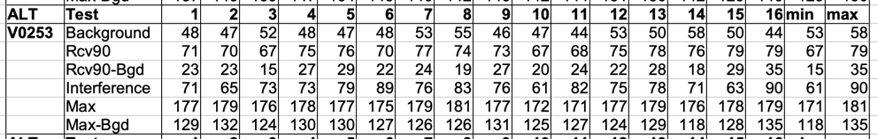
[08-DEC-22] We propose the following Quality Control Two (QC2) procedure. Configure the TCPIP interfaceRecord from TCB continuously with Neurorecorder. Play recording with Neuroplayer. Open Neurotracker window. Check Verbose, so we now see the top antenna power in the verbose output, as shown below. The "Tracker" line gives x, y, z position of the top antenna, as specified in the "alt" field of the NDF file's metadata. After that come sixteen values giving the detector module powers, all zero except for the top antenna.
Using 640 messages, including 128 clocks.
Channel 20,  0.0% loss, 512 reconstructed, 512 received, 0 bad, 0 missing.
Tracker: 48.0 8.0 2.0 0.0 0.0 0.0 0.0 0.0 0.0 0.0 178.0 0.0 0.0 0.0 0.0 0.0 0.0 0.0 0.0
In the lines above, the top antenna is number eight, assuming our mapping is correct from detector module to antenna input. The value "178" is the eight-bit digitized logarithmic power measurement provided by the top detector module. Connect metal-box test transmitter with center-frequency near 915 MHz via coaxial cable and attenuators to determine minimum input power for roughly 90% reception at each antenna input. Record this minimum along with the DM's own measurement of the same minimum power. Connect the same transmitter with no attenuator and record the maximum DM power measurement for saturated input. That's three numbers per detector module so far. Combine the signals from three metal-box test transmitters with center frequencies near 905 (LOW), 915 (MID), and 925 (HI) MHz using a four-way combiner with the fourth input terminated. Attenuate the combined signal so that power of each signal emerging is around −48 dBm, or some value that should be received by all TCB inputs. Apply this signal to all inputs and confirm that we see at least 90% reception from all three signals on each input. During this process, confirm that the detector module to antenna mapping is correct by watching the dots in the Neurotracker window, as shown below.
For each antenna input and each of the three bands LOW, MID, and HI, record the signal power at which we tested and succeeded in getting reception. If we fail to see 90% reception or greater, increase the power until we do see reception, and record that power. That's seven numbers per antenna input total. record in a table similar to those we make for the ALT.
We re-work the Message Receiver in P3042DM, eliminating its readout glitches. Now we obtain the following when we read out detetor module DM16, with all sixteen DMs running P3042DM V2.3, the controller running P3042BB V3.2.

We eliminate some delays and drop the message readout time to 8 μs in a scratch version of P3042BB. The first byte is enabled onto the daisy chain with the rising edge of DS. The rest by the falling edge. The delay between the edge of DS and data ready at the controller 400 ns from DM16. Allowing 200 ns at the start to let the target module establish itself, 400 ns for each of five bytes read out, we could in principle reduce the readout time to 2.2 μs. We plan to add a state machine to P3042BB that reads out the daisy chain as fast as it can and writes the bytes into a buffer. The controller's CPU can read these bytes out as they come in, and write them to the relay message buffer. Our hope is to increase the message rate to 200 kSPS.
[09-DEC-22] Detector module buffer running well. Improve efficiency of main loop. With the interface running off a 2 MHz clock, we are reading messages and processing them in 6.5 μs. We arrange for four detector modules to receive the signal from a single transmitter, a dual-channel 512 SPS. Reception is reliable and robust. We see around 1450 SPS when we expect 1152 SPS. When the CPU interrupt disturbs duplicate elimination we end up saving extra messages, and our Receiver Instrument is not configured to purge duplicates from our signal, but the lwdaq_receiver routine always eliminates duplicates, giving preference to the most powerful in a sequence of duplicates from a TCB. In the figure below we see four detector modules being read out sequentially, and at the end the top antenna message being written by the CPU to the main message buffer.

The CPU handles messages in roughly 3 μs running at 20 MHz in the LCMXO2-7000HC5. The detector module readout time of 6.5 μs is the rate-limiting step. We double the clock speed of the Detetor Module Interface, but the readout is no longer reliable. We reduce the size of the RAM. The logic now fits in the 2000HC. The HC version of the chip runs off a 3.3-V power supply. It comes in speed grades 4-6, with 6 being the fastest. These speed grades support CPU clock speed 21 MHz up to 24 MHz. The HE versions run off 1.2-V core power, but support 3.3-V I/O. They come in the same speed grades 4-6 and support the same 21 MHz to 24 MHz CPU clock. The ZE versions run off 1.2-V core with 3.3-V I/O, but their speed grade is 1 only, for which maximum clock speed is 10 MHz. Even with this slower chip, we will still maintain an average 6.5 μs per message, so our message rate will be 154 kSPS. Consider twenty 512 SPS transmitters in one Faraday canopy with eight antennas and another twenty in a second canopy, all conneted to our TCB-A16. If we obtain 100% reception from all antennas within each canopy our message rate will be around 160 kSPS. We tag P3042BB V3.3. Later, while examining a recording made with many transmitters, we see duplicates remain prominent.
Messages 0 to 10 (index id value timestamp $hex):
    0   0 34688 123 $0087807B 0000
    1 136 39167   4 $8898FF04 390B
    2 133 41627   4 $85A29B04 790C
    3  11 57171  12 $0BDF530C A801
    4 153 39407  33 $9999EF21 5A02
    5  20 40887  37 $149FB725 640C
    6 135 39604  39 $879AB427 390B
    7 135 39604  39 $879AB427 640C
    8  12 57431  43 $0CE0572B A801
    9  12 57431  43 $0CE0572B 9C0C
   10 134 41286  46 $86A1462E 790A
Most samples are being received by four detector modules. Roughly half the samples are recorded twice. We examine the code and the occurrance of the double-messages. The message handler checks DMBRDY. If it's clear, it prepares to save the previous message. But first it checks the previous message is valid, checks that MRDY is not set, and checks that DMBBUSY is not set. An interrupt might occurr during these instructions. By this point, it could be that DMBRDY is set, and there is another byte available. In V3.3 we do not check for DMBRDY again. We will introduce a second check of DMBRDY and see if it eliminates the duplicates.
[11-DEC-22] The second check of DMBRDY eliminates almost all duplicates. We record for 400 s minutes in M1670683616.ndf. Here is a typical eleven-message sequence.
Messages 0 to 10 (index id value timestamp $hex):
    0   0  4096 123 $0010007B 0000
    1  12 39827  10 $0C9B930A 8F0E
    2 133 41534  11 $85A23E0B A40A
    3  20 39628  12 $149ACC0C 8004
    4 135 39235  24 $87994318 830A
    5  41 43266  25 $29A90219 900A
    6  11 40583  27 $0B9E871B 8F0E
    7 119 41608  40 $77A28828 8608
    8 136 39069  51 $88989D33 830A
    9  12 40105  53 $0C9CA935 900E
   10 134 41155  71 $86A0C347 A402
There are duplicates in the first eleven message of each archive we create. Here are the first few milliseconds of M1670683616.ndf.
Messages 0 to 10 (index id value timestamp $hex):
    0   0     0 123 $0000007B 0000
    1 133 41439   6 $85A1DF06 880D
    2 133 41439   8 $85A1DF08 A40A
    3 135 39274  13 $87996A0D 830A
    4 119 41850  18 $77A37A12 8608
    5  41 42847  25 $29A75F19 900A
    6  11 40084  38 $0B9C9426 8F10
    7 136 39103  52 $8898BF34 840A
    8  12 39457  52 $0C9A2134 9A0A
    9  12 39457  63 $0C9A213F 8F10
   10  20 39531  74 $149A6B4A 8004
There are occasional duplicates in the rest of the recording. Here is an example at time 8.0 s.
   46 135 39247  79 $87994F4F 830A
   47  11 40266  79 $0B9D4A4F 8F10
   48 133 41415  80 $85A1C750 880D
   49 133 41415 104 $85A1C768 A40A
   50 136 39103 104 $8898BF68 6A02
   51 136 39103 111 $8898BF6F 840A
   52  12 40488 124 $0C9E287C 8F0E
[12-DEC-22] We apply an SCT signal −8 dBm through attenuators to obtain a plot of detector module power measurement versus SCT signal power. The detector module is loaded onto its base board in a TCB enclosure. The signal enters through one of the enclosure antenna connections, propagates across a straight feedthrough, and then along a UMCC cable to the detector module.

The plot stops at −62 dBm input, which is the minimum power at which the detector module can decode the incoming signal. Unlike the ALT, the TCB has no "background power" measurement for its antenna inputs, so we are unable to complete graphse like this.
[13-DEC-22] With one 512 SPS SCT signal fed into a single antenna input, we see perfect reception on the detector module but 50% reception by the base board. With our oscilloscope we observe that only half of messages are being stored. We find a bug in our CPU code where we have "jp z" instead of "jp nz". Correcting this error fixes our problem. We tag P3042BB 4V1, which we hope is ready for production.
[19-DEC-22] We arrange four antennas in an FE3A on a piece of wood, overlapping, so that we can place transmitter on all four at once and all four will carry their signals out of the enclosure. We split these four signals four ways each until we have sixteen antenna signals and feed them all into a single TCB-A16.

According to the lights on the sixteen detector modules, all sixteen receive every message from every transmitter, barring those blocked by collisions. When we reached 13 kSPS total sample rate, the red DMERR light illuminates on the display panel, see here. The detector module message buffers are overflowing. Our message rate is now 208 kSPS. At 200 kSPS the DMERR light does not turn on. We estimated the maximum message rate would be around 154 kSPS, we are pleased to see the TCB performing well up to 200 kSPS. Once the buffers are full, the TCB continues to operate. Some message are being lost, but it appears we still have at least one copy of each message. So it is not clear that this form of failure will lead to loss of data.
[23-DEC-22] Nathan examines the extent to which one TCB detector module will detect the signal fed into a neighboring detector module, and in particular how the two shield covers over the preamplifier and limiting amplifier will affect such cross-talk. He reports, "The lowest power input required to experience crosstalk in the TCB is −17 dBm and this is true with or without the shields on the detector modules."
We have eight antennas in an FE5A canopy and 14 kSPS of transmitters each being received by most of the antennas. The antennas are split into sixteen signals and fed into a TCB-A16. We see DMERR flashing. In the current firmware v2.3, a detector module asserts DMERR for one of three reasons: write to full buffer, read from empty buffer, or failure of its phase-locked loop (PLL) to lock to the incoming DMCK. The first two conditions are latched, so the DMERR light on the display panel will remain lit until reset. The PLL error, however, persists only so long as the failure to lock persists. The flashing DMERR light on the display panel, which we observed also previously, indicates intermittent failure of one or more detector module PLLs. We see the red light flashing on DM3 and later DM1 and DM2. The failure to lock stops when we turn off the transmitters and starts again when we turn them on again.
In the hours before we see the significance of the flashing DMERR light, we are examining the raw data from the TCB. We observe runs of duplicates spread over several clock ticks. In one case we observe the same message from the same detector module stored twice with different timestamps. We update detector module and base board firmware to delay or disable writing to all FIFO buffers when the buffers are full. Updating the base board firmware does not stop the duplicates. Our latest Receiver Instrument shows us raw messages and gives us a duplicate count we can watch as we are downloading the data. We are seeing 7k messages per half-second, containing 600 duplicates. These 7k are what is left of roughly 200k read from the detector modules after the base board's duplicate elimination. We re-program the detector modules starting at DM1 and working our way up to DM16. As we re-program a detector module, readout of the higher-numbered DMs is disabled and the duplicate count drops below 100. When we get to DM10, the duplicate count starts to rise. By the time we have reprogrammed all of them, the duplicate count is back to 600 and the red error lights are flickering on DM1 and DM2. We turn off the transmitters and the error lights turn off. With one or two transmitters in the enclosure, no detector modules fail to lock and duplicate elimination is perfect.
We suspect that activity on the daisy chain is inducing noise on DMCK. When the readout rate approaches 100 kSPS, we start to see failure to lock. The DMCK signal propagates from the base board logic chip past DM1 to DM16 and then to the display panel, where it reflects back to DM1. The DMCK signal is most corrupted by reflections at DM1 and DM2. It is these that fail to lock first. Right now we believe we have C48 = 100 pF loading DMCK at DM1 and 4 mA drive current from the base board logic chip.
[24-DEC-22] We remove C48. With 0 kSPS all DMs lock. At 5 kSPS DM1 fails to lock, and DM2-DM4 fail intermittently to lock.


We examine the clock at the start and end of a message readout using DMRC as our clock. We see no evidence that the readout is affecting the shape of DMCK. We let C48 = 100 pF and repeat. Once again, we see reliable lock with 0 kSPS, while at 5 kSPS DM1 always fails to lock and DM3 is intermittently locking.


At 5 kSPS we try 47 pF and 200 pF. In all cases we see reliable lock with 0 kSPS, while at 5 kSPS we have DM1 failing to lock.


The first few DMs will always lock if we remove any detector module up to and including DM10, but for DM11 and higher present, the lock is unreliable. We swap DM10 for a fresh DM and see the same behavior. We disconnect DM10's antenna and achieve the same effect as removing DM10. After ten minutes of making changes, we no longer see failure to lock in the first few DMs, but instead see buffer overflow in DM6, DM12, DM14-DM16. We have 5 kSPS entering all 16 antennas for total message rate of 80 kSPS. We record for 60 s. We see strings of duplicate messages in the recording. All DMs have new firmware that disables writing to the message buffer when the buffer is full.
We branch P3042DM and P3042BB to stream_configure branches in which we implement a configuration procedure following reset that allows the detector modules to determine their place in the daisy chain and remember it. The last DM in the chain is number one, and the first is number sixteen. Also branch P3042DM to quiet_read in which no ripple addition takes place, all DMs are number zero, so as to remove with minimal disruption the chaotic transisions caused by the asynchronous antenna number calculation on the daisy chain data bus.
[25-DEC-22] Reprogram all sixteen DMs with P3042DMQR1, quiet readout version one, in which we have no antenna number calculation and DM message buffers are only four messages deep. We place 5 kSPS in our Faraday canopy. We see no failure to lock. We see buffer overflow on DM16, DM15, and sometimes DM9-DM14. We reprogram DM12-DM16 with P3042DMQR2, in which detector module buffers are 32 deep. None of DM12-DM16 experience buffer overflow, but DM9-DM11 do overflow. No sign of flickering red lights on the detector modules, which implies no failure to lock. Continue until we have DM4-DM16 with buffers 32-deep, leaving DM1-DM3 4-deep. No buffer overflow. Increase sample rate in enclosure to 12 kSPS. Buffer overflow occurs immediately after reset, but we see no failure of detector modules to lock onto DMCK. Drop back to 5 kSPS. No buffer overflow, no failure to lock. The Receiver Instrument reports 4 kSPS downloaded, with 400 duplicates. Record 60 seconds in M1671988454.ndf. Leave the TCB running with the 5 kSPS to see if a overflow occurs over-night. Here is an example of duplication in the raw data, from the start of the recording.
   23  35 42092 205 $23A46CCD 640D
   24  12 39762 209 $0C9B52D1 A40D
   25  12 39762 210 $0C9B52D2 940D
   26  12 39762 210 $0C9B52D2 7A0D
   27  12 39762 210 $0C9B52D2 4B0D
   28  12 39762 211 $0C9B52D3 800D
   29  12 39762 211 $0C9B52D3 820D
   30  12 39762 212 $0C9B52D4 840D
   31  12 39762 212 $0C9B52D4 940D
   32  12 39762 213 $0C9B52D5 9D0D
   33  27 38830 231 $1B97AEE7 790D
   34  36 41759 239 $24A31FEF 630D
Here the antenna number is given always as 0x0D because the number reported by the DMs is zero, and the controller firmware maps number zero to TCB antenna input 0x0D = 13. We find a bug in the controller firmware, P3042BB. When the CPU reads the detector module buffer, we have been reading the input to the buffer (dmb_in) rather than the output (dmb_out). We correct and compile our master and self_configure branches of P3042BB.
[26-DEC-22] No DMERR on our TCB. Reprogram controller. No more consecutive duplicates in the raw data. Place a total of 11 kSPS in the Faraday canopy. The DMERR light turns on immediately. We suspect that some DMs may not have been re-programmed with the larger 32-deep buffer yesterday. We reprogram any that show an overflow. We record 60 s inM1672069013.ndf, no DMERR occurs. We appear to be reading roughly 150 kSPS. Our theoretical maximum message rate is 154 kSPS. Leave the TCB running overnight with 11 kSPS. We have several bugs in lwdaq_receiver, including one that crashes LWDAQ. We have disabled purging for our recording, and disabled duplicate replacement for TCB.
[27-DEC-22] No DMERR on TCB yet. Work on Receiver Instrument and Neurorecorder Tool to improve handling of errors. We purge duplicates in the Receiver Instrument for ODR and TCB, but not for ALT. We add to the Neuroplayer the option to purge duplicates from data it reads from an NDF file.
[04-JAN-23] Firmware P3042BB v4.2 provides a first effort at mapping the new daisy chain index to antenna socket on the box. Firmware P3042DM v3.1 implements configuration of daisy chain index after reset. We test both together. We see the antenna socket being calculated correctly from the index obtained during configuration. We see the index evolving as we reprogram detector modules and reset the TCB. The EMPTY and UPLOAD lights on the display panel are now behaving properly.
[24-JAN-23] We are exercising our six TCBs with reception tests, see here. We have three TCBs burned in. One we will keep here because of a problem with the enclosure, the other two are ready to ship.
[02-SEP-23] Six hours of recordings from three transmitters implanted in three mice, recorded with TCB-A16, reception plotted below, average 99.4% to 100.0%.

[26-SEP-23] Nathan describes Quality Control Three (QC3) for the TCB-A16 as follows. "We begin by setting three fully assembled TCBs on top of one another. The TCB on the bottom has already been through quality control and we are sure that it is up to standard. We then use BNC-T junctions in order to split each antenna signal into two different TCBs. This way, we get 4 half-antenna signals going to each TCB (see picture attached). Once the antennas are connected, we begin recording from all TCBs at once and wave 2 S2 transmitters as well as 2 A3 transmitters around the inside of the canopy randomly. Once recorded, we play back the recordings in the neuroplayer and use a processor script to measure the average reception from each transmitter every second. We average out the reception over 15 seconds and compare the two new TCBs to the old one which we know give adequate reception. Once we confirm the new TCBs give close enough reception to that of the old TCB, the new TCBs have passed QC3."

The idea of this test is to compare one TCB with another. With four antenna signals, each split between two TCBs, we are hoping for robust reception throughout the Faraday canopy, which is to say: we want average reception to be >95%. And indeed, in the test with Y71095 abnd Y71097, we see 94%-97% reception across three transmitters.
[25-OCT-23] We have four SCTs in boxes with connectors, each with a different center frequency. We have measured their power output. With attenuators, we can vary the SCT signal power we deliver to a combiner, in which we combine the SCT signal with a constant-frequency interference signal that we adjust to the center frequency of the SCT signal. For SCT signals −47 dBm to −5 dBm we measure the maximum interference power for which we can still obtain 90% SCT reception. We plot the ratio of interference power to signal power. This ratio is our interference tolerance.

The interference tolerance of the TCB is between −15 and −7 dBm for the range of signal powers we are likely to see on a telemetry antenna. The TCB's interference tolerance is roughly 3 dB lower than that of the Octal Data Receiver (A3027E).
[14-FEB-24] We are considering how best to construct 50-Ω tracks on a four-layer circuit board. Looking here, the thickness of the three dielectric layers will be 120 μm, 1.13 mm, and 120 μm. Naming the layers L1 to L4 from top to bottom, suppose we use L4 as signal and L3 as ground. A 0.31 mm track on L4 will combine with the ground on L3 to give 49 Ω impedance.
[15-FEB-24] We have 190-mAhr LiPo batteries with no protection circuit. They can appply 3.3 V to 2.7 Ω (1.2 A) for half a second, and 2.3 V to 0.68 Ω (3.4 A) for half a second. Our 3000-mAhr LiPo will apply 3.2 V to 0.68 Ω for one second (4.7 A). We order 380 mAhr and 240 mAhr LiPo batteries designed for drones and model helicopters. These claim to be able to provide 25C discharge, which for 380 mAhr is 9.5 A.
[16-FEB-24] We receive 240 mAhr, 30C LiPo batteries. They can deliver 1.2 A into 2.7 Ω, but their protection circuit disconnects the battery for 0.68 Ω load. We have 380 mAhr 25C from Tattu. These apply 3.6 V to 0.68 Ω for 5.3 A.
[22-FEB-24] We have five URGENEX 380-mAhr LiPo batteries rated 25C. As shipped, these apply 3.3 V to 0.68 Ω for 4.9 A. Consulting PowerStream's measurements of battery capacity versus charge voltage, we find that we get 90% capacity at 4.1 V, combined with no risk of over-charging. We choose 4.1 V for our A3042TF charge voltage.
[11-MAR-24] Transmitting Feedthrough (A3042TF) main board schematic complete, three pages, includes logic, power, battery, digital input-output, antenna switches, sockets for transmitter modules. Transmitter Module (A3042TM) schematic complete, one page, boost converter for LiPo voltage, power switch for amplitude modulation, SAW feedback oscillator to generate 915 MHz, medium-power amplifier with no output matching required to produce +24 dBm (300 mW), attenuator and low-pass filter to shape the square wave. Output is +22 dBm (160 mW) of 915 MHz. We start with the obsolete B3588 SAW filter in the oscillator because we know this one will work with a 50-mm track and an inverting amplifier. We have plenty of these on the shelf.
[29-MAR-24] Transmitting Feedthrough printed circuit board, part number A304202C, complete and submitted for fabrication.
[03-APR-24] Have first draft of Transmitter Module circuit board, part number A304204A. The 910-MHz oscillator in our A3029C used an ERA-3SM, phase advance +74° at 920 MHz. The physical length of the oscillator loop was 90 mm. Begin work on the Transmitter Module circuit board, part number A304204A. The oscillator amplifier is the GALI-3 from MiniCircuits. Its phase delay is +68° at 920 MHz. We expect to need roughly the same total loop length: 90 mm.
[23-APR-24] We are assembling our first A3042TF. We are unable to load U9 by hand, SiT1553 32.768 kHz in SMD-2012. We eliminate it from the design and instead produce 10 MHz × 8 ÷ 40 ÷ 61 = 32.787 kHz with the U6's internal PLL. This frequency is synchronous with our 10 MHz, generated by U10. We measure 32.794 kHz with our scope. We elimiante U9 from the design. We configure U6 to generate RESET when the TX line from the base board is HI for more than 39 ms.
[24-APR-24] Our digital output lines propagate 130, 170, 210, anc 250 mm down the board to the output drivers, for X1, X2, X3, and X4 respectively. When we enable with 10 MHz clock as data we see a clean 10 MHz on X1 and X2, but X3 and X4 rising edges have a constant glitch. At 32.8 kHz, the glitch persists. We load 100 pF from Q1..Q4 to 0V. We now see clean 10 MHz on all four outputs.

The digital output produces 2.2 V on a 50-Ω load, with clean edges at the far end. The highest frequency it can support is limited by the 100-pF capacitors to around 20 MHz. We enable all logic output drivers and set Q1-Q4 to LO so that we are terminating the incoming X1-X4 with 50 Ω. We drive X3 with 3-V 1-MHz square wave and see a clean value for D3 with rise time 250 ns. On TP4 we have D3 as output and we see a sharp-edged square wave with some edge jitter due to synchronization with FCK.
We check the operation of the battery connection, isolation, and charging. When we disconnect +5V, the battery always disconnects from the circuit. We discharger a LiPo and watch it charge up after connecting to VB. When we short VB our original R4=22Ω 1/4W overheats with 1 W dissipated. We make R4 P2010 3/4W 47Ω and add R18 the same. We load our 380 mAhr Tattu battery with 1 Ω on VB and see VB drop from 3.75 V to 3.55 V over 60 s while delivering 3.7 A. Thereafter, the battery starts to charge with 40 mA. We connect 0.5 Ω and see 3.25 V on VB, 3.48 on VB+. We measure 0.20 V directly across Q1, implying channel resistance 0.2 V ÷ 6.5 A = 31 mΩ for gate voltage −3.5 V, which agrees with the plots in the DMP2035U data sheet. We have Q1 dissipating 1.3 W. The package gets hot.
Load a blank A304204A transmitter module circuit board onto the A3042TF. Connector and mounting holes align. One 6-mm M2.5 standoff secures the board. We drive the ON bus with SCK and see the signal on our board, as well as VB.
[26-APR-24] Nathan writes, "We notice that while burning in the TCBs DMERR flashes intermittently. We determine this must be due to the phase loop failing to lock so we investigate how different modifications affect the signal at DC7. We try loading 100pF and 200pF at the source and at the other end and compare it to the signal without a mod. We find that the signal gets distorted if we put a base load capacitor on the opposite end of the source. Loading 200pF to ground on the opposite end of the source causes 2 of the detector modules to turn on their error lights. The error light goes away when touching a scope probe to DC7 at the source. Comparing all of these signals, we find that 200pF loaded at the source provides the smoothest 8MHz signal." Nathan is loading capacitors from DC7 to 0V to try to smooth the clock signal. He is measuring at the DC7 test point near the source of the signal.


[29-APR-24] Nathan increases the existing 100 pF at source to 200 pF on our three TCBs and we set up to burn in and look for DMERR flashing in the future.
[04-MAY-24] We have our first transmitter module, A3042TM-A. We are driving ON with 32.8 kHz. We drop R3 from its initial 10 kΩ to 1 kΩ and see the following response on VC.

We have 10 μs from the falling edge of ON to VC dropping to 2 V, at which point we can be confident that the RF output will be negligible. Looking at the command protocol for ISTs, the bit period is 122 μs, so our transmit ones will be 132 μs and our transmit zeros will be 112 μs. We reprogram the feedthrough logic to deliver ON = HI continuously. We remove C6 and R7. We deliver RF power to P2 and observe output on P3, using our hand-held generator and spectrum analyzer. We measure with 50 dBm attenuator on analyzer and 30 dBm and get output power measurements that differ by 4 dB.

[06-MAY-24] We load a UMCC plug onto the L4 footprint of our A3042TM-A so that we can feed a signal directly into U2. We remove R7 and C8. We use P2 to measure RA. We use our SSG-6001 synthesizer to provide 915 MHz through a cable and 2 dB attenuator. We plot RA power versus power delivered to L4.

We find that our spectrometer No1 reads −13.5 dBm when we deliver −10 dBm. Our SSG-6001 generator provides the same power as our RF Explorer signal generator. Both inputs on our No2 spectrometer read −10.5 dBm, so we believe we must add 3.5 dBm to measurements made with No1, which we have done for above plot. Our No3 spectrometer (6GHz) reads −8.0 dBm on its wide-band input and −5 dBm on its narrow-band input.
With C2 = 22 μF we see 150 mVpp 100 kHz ripple on VC. With 88 μF we see 50 mV. We load 51 kΩ in parallel with R2=10kΩ and see VC = 5.7 V. With C2 = 22 μF ripple is 40 mVpp. With −10 dB delivered to L4 we see 23 dBm on T. We drop VC back to 5.0 V and see 22 dBm on T.
We connect remove our L4 connector and load B3588. We try 51 Ω, 100 Ω, and 330 Ω for R7, loading a new B3588 each time. No oscillation. We connect L4-2 to R6 with a shorter path. We see oscillation at 915.4 MHz, output power at T is +23.5 dBm. We try SF2098E SAW filter and get 911.8 MHz and 23.5 dBm. Both these filters can tolerate +15 dBm input. The maximum power at RA is +14.5 dBm in our measurements. With R7 = 51 Ω in series with 50-Ω input of U2, as well as the 50-Ω input of U3 in parallel, we guess U2-1 will see +5 dBm. Return to B3588. Output spectrum consists of one peak at 915 MHz of 21.5 dBm and another at 1830 MHz of −31 dBm.
We put T through −20 dB and mix with 865 MHz. We look at the IF on our scope. We set ON to a 2-kHz square wave. Oscillation in the A3042TM does not start up unless we place a finger on the feedback resistor. The unused delay trace to the R7 footprint is acting as a 20-mm open-circuit stub. We cut the trace to remove the stub. We now see reliable turn-on of the 915 MHz after the rising edge of ON.

Turn-on to full power takes around 700 ns from rising edge of ON. Turn-off takes around 7 μs from falling edge of ON.

The amplitude of the IF is 300 mVpp, or −6.5 dBm. Loss in ZAD-11 is around 7.5 dB, and we have 20-dB attenuator, so our T output from this measurement is around +21 dBm. In our experience, these ZAD-11 power measurements are accurate to ±1 dB.
We connect T to T1 on our A3042TF-A. We have D and T the wrong way around on the feedthrough: ON connects A1 and D1. We want ON to connect A1 and T1. Our 380-mAhr LiPo battery ran down providing current for our A3042TM. We disconnecdt the A3042TM and leave power and battery connected to the A3042TF to see if the battery will re-charge.
[07-MAY-24] Voltage on our battery has reached 4.16 V. We replace Q2 on the A3042TM-A with SN74LVC1G125 powered off VC. Now ON becomes !ON. The gate of Q1 is driven HI by the buffer, making the turn-off fast, see below.


We note that 3.0-V logic is not guaranteed to meet the HI logic threshold of the 74LVC1G125 when VCC = 5.0 V. We plan to raise the logic supply on the A3042TF-A from 3.0 V to 3.3 V with the TLV71333 for U8. Our battery voltage is 4.08 V with ON asserted half the time. We connect T to T1 and the HI voltage of !ON1 drops from 3.0 V to 2.0 V. Disconnect, and it is restored. With !ON1 never rising above 2.0 V, the RF on T never turns off. We remove U17 and load a new PE4259, making sure it is the right way around. Previous part was micropower PE4239DS, and we did not check orientation was correct before removal. Now !ON behaves correctly. We connect T to T1 and look at A1 at turn-on.

We see IF 270 mVpp = −7 dBm. Add 27 dB loss in attenuator and mixer and we are seeing 20 dBm coming out of A1. While U17 is directing T1 to A1, we look at D1 to see signal leaking through the switch.

We see a burst of higher power, then 50 mVpp = −22 dBm. Add 9 dB loss in attenuator and mixer and we are seeing −13 dBm at D1. Isolation through the switch is around 33 dB. Typical value for this switch is 30 dB. The ON and OFF switching times are given as 1.5 μs, which explains the burst of RF we see starting 750 ns after ON asserted, and going on for 750 ns. The peak power in this burst is +4 dBm. The A3038DM-D3 to which D1 will connect presents the incoming signal with a 2-dB attenuator and then the input of BGA2803. This amplifier can tolerate +10 dBm. The maximum burst it will receive is 2 dBm.
We turn on T1 continuously and measure 918 MHz with our No2 spectrometer, 20.5 dBm. Out of D1, −23 dBm. Current flowing into 5V0 is 125 mA, into VB is 160 mA at 3.8 V. Remove TM No1. We see 37 mA from VB into the battery, 5V0 = 5.0 V and VB = 3.9 V. Remove battery, 70 mA flows into 5V0. From these numbers we deduce that 255 mA from the battery is required to power a single A3042TM. At 3.8 V, that's 817 mW. Quiescent current of the GVA-92 and GALI-3 combined is 135 mA at 5.0 V for 675 mW. Our TLV61048 is providing 83% efficiency. Power output at U3-3 is roughly 24 dBm = 250 mW, so the module is 37% efficient at turning electrical power into RF power.
Add a few millimeters to feed back wire, put resistor on R6 directly. Output drops frm 918 to 916 MHz. Shorten wire again, 916 MHz. Wash and dry, back to 918 MHz. The tuning of the A3041 is centered on 915 MHz, with ±10 MHz acceptable.
[10-MAY-24] Prepare A304401B for fabrication. This new layout replaces Q2 with U4, the logic buffer. We add P5 to permit us to feed power into U2. We rotate U1 so that U1 and U4 have the same upright orientation. We shorten the RA feedback path from 50 mm to 30 mm. We mark the incoming control as !ON.
[12-MAY-24] We are preparing P3044BB5V1, in which we will implement communication with the A3042TF. When testing existing functions in the new code, we connect one antenna to DM6, excite with a 2048 SPS SCT, and find that max_block_reads = 20 is insufficient for download from the TCB. We revert to BB4V3 firmware, same problem. We increase max_block_reads to 50 for ALT and TCB. Code BB5V1 is stable for existing functions.
[13-MAY-24] We load our A3042TF-A1 into a TCB enclosure and connect to the A3042BB-D2 base board with a harness of four wires. We have TP3 commandeered as TX and TP4 as RX. We have +5V coming from the base board through P1.

We route A1 through to D1 by unasserting !ON1. We connect D1 to a detector module. We obtain robust reception of an SCT through the A3042TF. We exercise TX with a serial transmission and examine the rising and falling edges at their source on the base board and at their destination on the transmitting feedthrough. The two signals suffer no significant overshoot, rise time is 5 ns, delay 3 ns.
