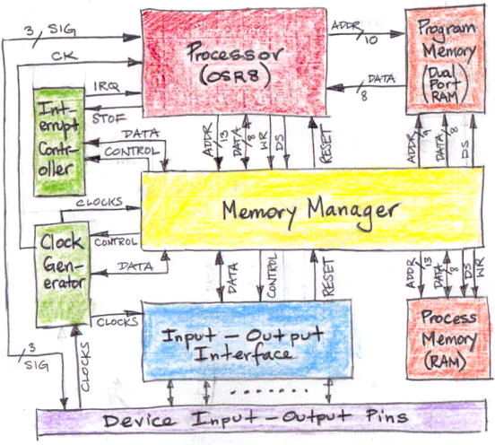
Figure: OSR8 and Peripheral Logic for Embedded Controller on a Single Chip. Address sizes shown are those of the A3035A application, but may be up to sixteen bites wide.
[12-DEC-20] The OSR8 is an open-source, reconfigurable eight-bit processor described in VHDL (virtual hardware description language) for implementation in programmable logic devices. The processor is designed to be small and energy-efficient. We want the OSR8 to fit in the logic chip we have available on a small battery-powered circuit, and we want it to perform calculations with the minimum energy consumed from the battery. When we implement the The OSR8V1 with 16×1-bit look-up tables (LUTs), as in the MachXO2 Family of programmable logic devices, the OSR8V1 occupies 800 LUTs. A practical application of the OSR8 will, however, require another 400 LUTs for peripheral logic, as well as memory blocks to store programs and data. The A3035A application uses all 7 embedded function blocks and 1246 of the 1280 LUTs provided by its 2.5-mm square LCMXO2-1200ZE. When running at 5.0-MHz using its own ring oscillator, the OSR8 and ring oscillator together consume 2.3 mA while delivering one hundred and fifty thousand eight-bit multiplications per second (150 kMPS). When running off an external, micropower 32.768-kHz oscillator, it consumes 100 μA from 1.2 V while delivering 1 kMPS.
The OSR8V1 provides seven eight-bit registers, A, B, C, D, E, H, and L, and a flags register, F. The flags are zero (Z), sign (S), carry (C), and interrupt (I). The OSR8V1 provides two index registers, IX and IY, that we use to hold process memory pointers for moving bytes between process memory and the registers. It provides a stack pointer, SP, and of course a program counter, PC to step through the instructions stored in its program memory. It provides eight-bit addition of A and B or of A and a constant n, it provides separate increment and decrement functions for all registers, index pointers, and the stack pointer. It provides a variety of shift and rotate operations that facilitate multiplication and long additions. It provides logical AND, OR, and XOR between A and B or A and a constant n. The OSR8 assembly language is similar to that of the Z80 in the way the instructions are written out. Unlike the Z80, however, the OSR8 uses big-endian byte ordering (most significant byte at the lower addres) and its stack is upward-extending, so when we push a byte onto the OSR8 stack, we increment the stack pointer and write the byte to the process memory location pointed to by the incremented stack pointer.
The processor is a single VHDL entity implemented entirely with look-up tables and registers. It communicates with the outside world through the signals shown in the diagram above. All other components of the embedded controller are provided by entities external to the processor. In the A3035A, the program and process memory are proviced by embedded function blocks in the LCMXO2-1200ZE. The program memeroy is a 1-KByte of ROM loaded with the program, while the process memory is 6-KBytes of RAM loaded at start-up with accelerometer initialization bytes. All other peripheral logic in the A3035A application is defined in VHDL and implemented with look-up tables.
The program memory contains the instructions to be executed by the processor. The processor reads the program memory directly with its program counter one byte at a time. The processor accesses all other peripherals through the memory manager by means of the processor address and data buses. The processor implements a bi-directional eight-bit data bus with eight outgoing data bits and eight incoming data bits. The processor clock, CK, is provided by the clock generator, which it controls through the memory manager. In the micro-power ORS8 applications, the clock generator can switch CK betweek 32.768 kHz provided by an external micropower crystal oscillator, and 5.0 MHz provided by an internal, calibrated ring oscillator. The processor uses the rising edge of the clock to set up its program counter, processor address, outgoing processor data, and all control signals. It uses the rising edge to store incoming processor data. In all existing OSR8 applications, we read the program memory on the falling edge of CK. The memory manager should act on the falling edge of CK for read cycles, and can use the falling edge or rising edge of CK for write cycles. By using both edges of CK, the processor is able to perform register-only instructions in one clock cycle. When the MMU implements a writeable program memory, the processor read cycles must take place on the opposite edge from the write cycles. We read instruction bytes from propram memory on the falling edge of CK and write instructions into the user program memory on the rising edge.
The A3035 provides no connection between the memory manager and the program memory, so the processor runs only programs that were written to its non-volatile configuration memory at the time the device was programmed. The device may not be reprogrammed once it is encapsulated. The A3041 provides write-only access to the program memory through the memory manager, which allows the processor to receive programs through its crystal radio and write them to a section of its program memory reserved for the purpose.
A single interrupt request input, IRQ, will interrupt the processor, provided the processor's interrupt flag (I) is not set. The interrupt controller provides interrupt bits for various interrupt sources, mask bits to enable or disable assertion of IRQ by these individual interrupt bits, as well as set and reset bits that the processor can use to clear and assert interrupts. The A3035A application provides an interrupt timer that can be configured by the processor to generate regular interrupts. The stack pointer overflow output, STOF, indicates to the interrupt controller that the processor's internal stack has overflowed, which should generate an interrupt with IRQ.
The RESET input to the processor will reset its stack pointer and program counter and re-start program execution from the starting address. In the A3035A, the start address is 0x0000, and the interrupt address, to which the processor jumps upon servicing an interrupt, is 0x0003. Both locations should be occupied by an unconditional jump instruction that takes the processor to the correct program. The OSR8 "jp nn" instruction occupies three bytes. The OSR8 has no reset instruction. The A3035A application provides a software reset bit the processor can set to cause RESET to be asserted for one CK period.
Additional internal controller functions may be added and made available to the OSR8 through the Memory Manager. The A3037B provides an eight-bit multiplier to accelerate EEG signal analysis. The processor writes two bytes to two locations, and reads our the product from to additional locations.
The input-output interface provides access to external circuit components. In the A3035A application, the interface provides logic to read and write from an accelerometer and a gyroscope, and to transmit sixteen-bit samples through the radio-frequency antenna. These functions are made available to the processor by the memory manager in the form of eight-bit memory locations. To write a sixteen-bit word to the accelerometer, for example, the processor writes the high and low bytes to two separate locations, the accelerometer register address to a third location, and a code number to a control register to initiate the write cycle. In the A3037B, the processor turns on the implantable lamp attached to the A3037B's stimulus leads by writing to a register, and turns off the lamp by writing to the same register.
The input-output pins are the signals present on the device pins. The processor provides three re-configurable signals SIG0..SIG2 that may be connected directly to the device pins. In the A3035A, these three signals are outputs that encode the state of the processor, and so may be used for debugging program execution. But the SIG signals could be re-configured to act as copies of internal CPU signals, or as inputs to the CPU for new instructions added to the OSR8 for new applications.
[13-DEC-14] The processor is defined in a single VHDL file OSR8Vn.vhd, where n is version number. We include OSR8Vn.vhd in our firmware. We maintain a master copy of each version in the OSR8 repository. We configure the OSR8 with generic constants when we instantiate the CPU in our firmware architecture. The table below lists some applications of the OSR8. Click on the OSR8 link to go to the device's firmware repository.
| Version | Platform | Size (LUTs) |
Features | Application with Clock Frequency |
|---|---|---|---|---|
| OSR8V3 | Any | 800 | User-Configurable | Generic V3 code |
| OSR8V3 | LCMXO2-1200ZE WLCSP-25 | 800 | 6 KB RAM, 1 KB ROM, 5.0 MHz. | Implantable Inertial Sensor (A3035A) |
| OSR8V3 | LCMXO2-7000HC TQFP-144 | 950 | 6 KB RAM, 8 KB ROM, 20 MHz. | Animal Location Tracker Base Board (A3038C) |
| OSR8V3 | LCMXO2-1200ZE WLCSP-25 | 850 | 4 KB RAM, 4 KB ROM, 5.0 MHz with user program memory |
Implantable Stimulator-Transponder (A3041A) |
| OSR8V3 | LCMXO2-7000HC TQFP-144 | 850 | 2 KB RAM, 4 KB ROM, 20 MHz | Telemetry Control Box Base Board (A3042BB) |
| OSR8V3 | LCMXO2-1200ZE WLCSP-25 | 800 | 1 KB RAM, 4 KB ROM, 5 MHz. | Fiber Controller (A3045) |
The peripheral functions of each application are defined in separate files specific to the application. The links in the application column of the table above lead to circuit manuals.
Here is an example OSR8 program written in the OSR8 Assembly Language. When this program runs in the A3035A application, it generates a square wave on pin P1-1 of the programming extension.
const mmu_tpr  0x1E38 ; Test Point Register
main:
ld A,0x01        ; 2 Load A with bit zero set to one.
ld (mmu_tpr),A   ; 3 Set the test point one bit.
ld A,0x00        ; 2 Load A with all bits zero.
ld (mmu_tpr),A   ; 3 Clear the test point one bit.
jp main          ; 3
The program begins with the declaration of a sixteen-bit constant giving the address in process memory of the test point register, which the OSR8 can use to set the logic level on TP1 in the A3035A. The main loop sets bit zero of the test point register to HI and then LO before jumping back to start over. We show the number of clock cycles used by each instruction in the loop. The entire loop takes 13 clock cycles, and the clock is 32.768 kHz so the square wave will run at 2.52 kHz and its HI pulse will be 152 μs.
In OSR8 assembly, each instruction is presented on a single line of assembly code. The first word in an instruction line is the operation code, or opcode. After that there may be two operands separated by commas. We use parenthesis to show that an operand should be used as an address to access a byte in process memory. When we load a register with the operand itself, we refer to the operation as a direct load. When we use the operand as an address to look up a value to load into a register, we refer to the operation as an indirect load. Thus "ld A,4" is a direct load of register "A" with the constant "4", while "ld A,(0x0123)" is an indirect load of register "A" with the contents of memory address "0x0123". On any line, every character after a semicolon is a comment and will be ignored by the assembler. The language is insensitive to case, so you may use lower-case or upper-case letters as you like. The following line specifies the eight-bit indirect load of the accumulator from address 0x1702.
ld A,(0x1702) ; Load A with HI sensor byte.
We specify a location in program memory to which we can jump to, we use any any string containing letter and underscores followed immediately by a colon, and place this label just before the location we wish to label. The label must be alone on its declaration line. When we later mention the label, we do not include the colon, so as to distinguish between the definition of the label and the use of the label.
loop:        ; We can put a comment here too
dec A        ; Decrement the accumulator
jp nz,loop   ; Jump to loop if accumulator is not zero
Jump points are global constants that can be declared anywhere and referred top anywhere. So we can refer to a jump point in an instruction before we declare it.
dec l       ; Decrement register L
jp nz,notz  ; If L is not zero, jump over the decrement of H
dec h       ; Decrement register H
notz:       ; This is where we declare the label "notz"
adc A,56    ; Add 56 decimal to the accumulator, with carry.
Empty lines, or lines with only comments, are ignored by the assembler, although they are counted, so that warning and error messages will be able to refer to the correct line number. To declare a constant use the following notation.
const sensor_hi 0x1702 ; Define sensor_hi to be value 1702 hexadecimal.
const step_size 34     ; Replace "step_size" with 34 decimal.
ld A,step_size         ; Load step-size constant into the accumulator
ld (sensor_hi),A       ; Load byte location sensor_hi with accumulator.
All constants in OSR8 assembly are global constants and must be declared before they are used. All labels are global labels, but they may be declared after they are used. In the following program, we see the labels "main" and "interrupt" are used before they are defined.
start:
jp main
jp interrupt
interrupt:
rti
main:
jp main
The "start" label marks the address at which program execution will begin. In the A3035A application, this address is 0x0000. When the OSR8 is interrupted by IRQ or an "int" instruction, it jumps to a pre-defined interrupt address in program memory. In the A3035A application, this interrupt address is 0x0003. The value 0x0003 is convenient because the "jp main" instruction occupies three bytes, so the "jp interrupt" we can put immediately after "jp main" and the two instructions will be correctly located in program memory for start-up and interrupts. We see that the "main" and "interrupt" labels are referenced before they are defined.
[01-JUL-22] The OSR8 status flags are zero (Z), sign (S), carry (C), and interrupt (I). Mathematical and logical operations set the flags. Load, push, and pop operations do not. In our description of each instruction, we state which flags the instruction sets. We present the flags in detail here. The Z, S, and C flags are set by the action of the OSR8's arithmetic logic unit (ALU). The ALU is an eight-bit adder, subtractor, and logical operator. The Z flag is set when the eight-bit result of an operation is all zeros. Here are some examples.
and A,0xFF ; When A=0, Z will be set.
add A,0 ; When A=0, Z will be set.
sub A,7 ; When A=7, Z will be set.
xor A,0xFF ; when A=0.FF, Z will be set.
add A,0 ; When A=1, Z will not be set.
add A,1 ; When A=0xFF will be set.
When the result of an addition overflows the eight-bit output of the ALU, a ninth bit, called the carry bit is set, as if the output of the ALU were a nine-bit number. When the result of subtraction underflows zero, the carry bit is once again set, to represent a borrow bit. The C flag is set whenever this carry or borrow bit is set. When we add one to 0xFF we get 0x00 with the carry bit set. So we have the Z flag set, and we also have the C flag set.
and A,0xFF ; C will never be set.
add A,0 ; C will never be set.
sub A,7 ; When A<7, C will be set.
add A,23 ; When A>=233, C will be set.
The S flag is for two's-compliment arithmetic, where we represent negative integers by taking the positive integer, negating its bits and adding one. We would negate an integer like this:
xor A,0xFF ; Negate all bits
add A,1 ; and add one.
In the above example, +1 becomes 0xFF, which is the two's compliment representation of −1. When we add +1 and −1 together we get zero with a carry. The eight-bit ALU inputs and outputs, when used for signed integert arithmetic, represent values −128 to +127. The negative values are those with the top bit set. The S flag is set equal to the top bit of the ALU result after a mathematical or logical operation. We intend the N flag to mean, "The result of the most recent two's compliment addition or subtraction is less than zero".
The OSR8 provide conditional jump commands controlled by the Z, S, and C flags. The "S" flag we refer to in these commands with "p" for "positive" and "np" for "not positive". By "positive" we mean "zero or greater", which is "0..127". By "not positive" we mean "less than zero".
ld A,65 ; Load 0x41 into A.
add A,76 ; Add 0x4C to A. Sum is 141, 0x8D, or -115.
jp np,later ; We will jump.
The I flag is the "CPU running in interrupt mode" flag. The I flag is set automatically by the execution of an interrupt, but we can also set it with the seti instruction, and clear it with clri. When the CPU sets I, we think of it as saying that it is already handling an interrupt, so no other interrupt should do any further interrupting. When we clear the I flag, we are saying that interrupt handling is over, and a new interrupt can commence.
The OSR8 is a reduced instruction set computer (RISC). The OSR8V1 provides an instruction set that is sufficient to perform any arithmetic or multi-tasking function, and includes some instructions that facilitate efficient execution of loops and block moves in memory, but does not include many standard instructions that abbreviate assembly programs and accelerate execution. The OSR8V1 provides instructions to push and pop all its seven registers to and from the stack, but it does not provide any operations to load one register directly with the contents of another, nor to exchange the values of two registers. It provides operations to load register A with a constant, or with the contents of a particular memory location, but it does not operations to do the same for the other registers, although it does provide an operation to load register pair HL with a constant nn. This latter instruction the OSRV1 requires if it is to implement interrupt-driven multi-tasking. The multi-tasker needs some way to load a value into the stack pointer without using the stack.
| Syntax | Opcode | Syntax | Opcode | Syntax | Opcode | Syntax | Opcode |
|---|---|---|---|---|---|---|---|
| nop | 0x00 | jp nn | 0x01 | jp nz,nn | 0x02 | jp z,nn | 0x03 |
| jp nc,nn | 0x04 | jp c,nn | 0x05 | jp np,nn | 0x06 | jp p,nn | 0x07 |
| call nn | 0x08 | int | 0x09 | ret | 0x0A | rti | 0x0B |
| wait | 0x0C | clri | 0x0D | seti | 0x0E | ld A,n | 0x10 |
| ld IX,nn | 0x11 | ld IY,nn | 0x12 | ld HL,nn | 0x13 | ld A,(nn) | 0x14 |
| ld (nn),A | 0x15 | ld A,(IX) | 0x16 | ld A,(IY) | 0x17 | ld (IX),A | 0x18 |
| ld (IY),A | 0x19 | ld HL,SP | 0x1A | ld SP,HL | 0x1B | ld HL,PC | 0x1C |
| ld PC,HL | 0x1D | push A | 0x20 | push B | 0x21 | push C | 0x22 |
| push D | 0x23 | push E | 0x24 | push H | 0x25 | push L | 0x26 |
| push F | 0x27 | push IX | 0x28 | push IY | 0x29 | pop A | 0x30 |
| pop B | 0x31 | pop C | 0x32 | pop D | 0x33 | pop E | 0x34 |
| pop H | 0x35 | pop L | 0x36 | pop F | 0x37 | pop IX | 0x38 |
| pop IY | 0x39 | add A,B | 0x40 | add A,n | 0x41 | adc A,B | 0x42 |
| adc A,n | 0x43 | sub A,B | 0x44 | sub A,n | 0x45 | sbc A,B | 0x46 |
| sbc A,n | 0x47 | clrf | 0x4F | inc A | 0x50 | inc B | 0x51 |
| inc C | 0x52 | inc D | 0x53 | inc E | 0x54 | inc H | 0x55 |
| inc L | 0x56 | inc SP | 0x57 | inc IX | 0x59 | inc IY | 0x5A |
| dec A | 0x60 | dec B | 0x61 | dec C | 0x62 | dec D | 0x63 |
| dec E | 0x64 | dec H | 0x65 | dec L | 0x66 | dly A | 0x67 |
| dec SP | 0x68 | dec IX | 0x69 | dec IY | 0x6A | and A,B | 0x70 |
| and A,n | 0x71 | or A,B | 0x72 | or A,n | 0x73 | xor A,B | 0x74 |
| xor A,n | 0x75 | rl A | 0x78 | rlc A | 0x79 | rr A | 0x7A |
| rrc A | 0x7B | sla A | 0x7C | sra A | 0x7D | srl A | 0x7E |
The assembler lists all instructions defined by all versions of the OSR8. Before we attempt to include instructions in our assembly code for a particular OSR8 application, we must make sure that the application's OSR8 version provides the instruction. We define the complete set of instructions below. For each instruction, we state what flags are affected by the instruction, and how they are affected. If we do not mention a flag in the description of an instruction, it is unaffected. We also give the number of clock cycles required to execute the instruction.
nop: No operation. Increment the program counter and read the next operation code. Clock cycles: 1.
jp nn: Unconditional jump to location nn in program memory, where nn is a two-byte address. Clock cycles: 3.
jp nz,nn: If the zero flag (Z) is not set, jump to location nn, otherwise proceed to the next instruction. Clock cycles: 3.
jp z,nn: If the zero flag (Z) is set, jump to location nn, otherwise proceed to the next instruction. Clock cycles: 3.
jp nc,nn: If the carry flag (C) is not set, jump to location nn, otherwise proceed to the next instruction. Clock cycles: 3.
jp c,nn: If the carry flag (C) is set, jump to location nn, otherwise proceed to the next instruction. Clock cycles: 3.
jp np,nn: If the sign flag (S) is set, jump to location nn, otherwise proceed to the next instruction. The sign flag is set when the result of an addition, subtraction, or decrement is negative in two's compliment arithmetic, which is true if and only if the top bit of the eight-bit result was set. The pneumonic "np" means "not positive". We cannot use "n" for "negative condition" and "nn" for "not negative", because we have already reserved these letters in our pneumonic definitions. So we use "p" for positive and "np" for not positive. Clock cycles: 3.
jp p,nn: If the sign flag (S) is not set, jump to location nn, otherwise proceed to the next instruction. See above for why we use "p" for "not negative". Clock cycles: 3.
call nn: Call the subroutine that begins at program location nn. The OSR8 will push the program counter onto the stack, HI byte first, LO byte second, then jump to the specified location. Clock cycles: 3.
int: Jump to the interrupt location, which is equivalent to calling the interrupt routine. Push the program counter onto the stack and jump to the interrupt location. We don't have to specify this location in the instruction because the interrupt location is a fixed location. In the OSR8V1, the interrupt location is 0x0003. The int instruction does not set flag I. Clock cycles: 2.
ret: Return from subroutine. Pop the program counter off the stack, LO byte first, HI byte second, increment the program counter, and so execute the next intruction after the "call" instruction we assume was used to execute the subroutine from which we are returning with "ret". Clock cycles: 4.
rti: Return from interrupt. Pop the program counter off the stack, LO byte first, HI byte second. We are returning from executing the interrupt routine. If we jumped to the interrupt routine in response to IRQ being asserted, the OSR8 avoided executing an instruction, set the interrupt flag, I, and pushed the program counter onto the stack. The interrupt routine must refrain from clearing the I flag, so that I will still be set upon execution of rti. The OSR8 assumes that rti is returning from an IRQ-provoked interrupt if and only if I is set. It pops the program counter off the stack, does not increment the program counter, clears I, and continues execution of the interrupted process. If we called the interrupt routine with an int instruction, the I flag must not be set upon execution of rti. The OSR8 will pop the program counter off the stack, increment the counter, and continue execution of the interrupted process at the instruction after the int that called the interrupt routine. An interrupt routine that we intend to execute in response to both IRQ and int can set I to prevent itself from being interrupted by IRQ, but it must restore I to its original state before rti. The interrupt routine can obtain the current state of I with push F and pop A, and it can clear and set I with clri and seti. Clock cycles: 3 when flag I is set, 4 when flag I is not set.
wait: Clear the I flag so as to enable interrupts, but otherwise do nothing. Do not increment the program counter, but keep executing this instruction until IRQ or RESET is asserted. When IRQ is asserted, execute the interrupt routine, then return to the wait instruction. Clock cycles: 1.
clri: Clear the I flag to zero, thus enabling interrupts. Clock cycles: 1.
seti: Set the I flag to one, thus disabling interrupts. Clock cycles: 1.
ld A,n: Direct load of A. Load register A with the single-byte value n. Clock cycles: 2.
ld IX,nn: Direct load of IX. Load index register IX with two-byte process address value nn. Clock cycles: 3.
ld IY,nn: Direct load of IY. Load index register IY with two-byte process address value nn. Clock cycles: 3.
ld HL,nn: Direct load of HL. Load register pair HL with two-byte constant nn, where the HI byte of the constant is loaded into H and the LO byte is loaded into L. Clock cycles: 3.
ld A,(nn): Indirect load of A. Read the byte at process memory location nn and load it into register A. Clock cycles: 4.
ld (nn),A: Indirect load from A. Write the byte in register A to location nn in process memory. Clock cycles: 3.
ld A,(IX): Indexed load of A using IX. Read the byte at location IX in process memory and load it into A. Clock cycles: 2.
ld A,(IY): Indexed load of A using IY. Read the byte at location IY in process memory and load it into A. Clock cycles: 2.
ld (IX),A: Indexed load from A using IX. Write the byte in register A to location IX in process memory. Clock cycles: 1.
ld (IY),A: Indexed load from A using IY. Write the byte in register A to location IY in process memory. Clock cycles: 1.
ld HL,SP: Direct load of register pair HL with stack pointer SP. The HI byte of the stack pointer, SP, is loaded into H and the LO byte is loaded into L. Clock cycles: 1.
ld SP,HL: Direct load of SP with HL. The HI byte of the stack pointer, SP, is loaded with H, and the LO byte of SP is loaded with L. Clock cycles: 1.
ld HL,PC: Direct load of HL with PC. The HI byte of the program counter, PC, is loaded into H, and the LO byte of PC is loaded into L. Clock cycles: 1.
ld PC,HL: Direct load of PC with HL. The HI byte of the program counter, PC, is loaded with H, and the LO byte of PC is loaded with L. Clock cycles: 1.
push A: Push A onto the stack. Increment the stack pointer, SP, by one and write A to the process memory location given by the incremented value of SP. Clock cycles: 1.
push B: Push B onto the stack. Increments SP by one. Clock cycles: 1.
push C: Push C onto the stack. Increments SP by one. Clock cycles: 1.
push D: Push D onto the stack. Increments SP by one. Clock cycles: 1.
push E: Push E onto the stack. Increments SP by one. Clock cycles: 1.
push H: Push H onto the stack. Increments SP by one. Clock cycles: 1.
push L: Push L onto the stack. Increments SP by one. Clock cycles: 1.
push F: Push the flags register onto the stack. The values of the Z, S, C, and I flags will be copied to the stack. We push the flags onto the stack when we begin an interrupt routine that will change the flags. Increments SP by one. Clock cycles: 1.
push IX: Push IX onto the stack. The HI byte will be pushed first, and the LO byte second. Increments SP by two. Clock cycles: 2.
push IY: Push IY onto the stack. The HI byte will be pushed first, and the LO byte second. Increments SP by two. Clock cycles: 2.
pop A: Pop A off the stack. Read the byte at the process memory location pointed to by the stack pointer and load it into A, then decrement the stack pointer. Decrements SP by one. Clock cycles: 2.
pop B: Pop B off the stack. Decrements SP by one. Clock cycles: 2.
pop C: Pop C off the stack. Decrements SP by one. Clock cycles: 2.
pop D: Pop D off the stack. Decrements SP by one. Clock cycles: 2.
pop E: Pop E off the stack. Decrements SP by one. Clock cycles: 2.
pop H: Pop H off the stack. Decrements SP by one. Clock cycles: 2.
pop L: Pop L off the stack. Decrements SP by one. Clock cycles: 2.
pop F: Pop F off the stack. Pop the flags off the stack. We pop flags off the stack at the end of an interrupt routine that affects the flags. Decrements SP by one. Clock cycles: 2.
pop IX: Pop IX off the stack. The LO byte will be popped first, and the HI byte second. Decrements SP by two. Clock cycles: 3.
pop IY: Pop IY off the stack. The LO byte will be popped first, and the HI byte second. Decrements SP by two. Clock cycles: 3.
add A,B: Add register B to register A, leaving the result in A. If the sum exceeds 0xFF, set the carry flag (C), otherwise clear C. If the sum is zero, set the zero flag (Z), otherwise clear Z. If the sum is negative, set the sign flag (S), otherwise clear S. Clock cycles: 1.
add A,n: Add constant n to register A, leaving the result in A. If the sum exceeds 0xFF, set C, otherwise clear C. If the sum is zero, set Z, otherwise clear Z. If the sum is negative, set S, otherwise clear S. Clock cycles: 2.
adc A,B: Add register B to register A with carry in, leaving the result in A. If C is set, add one to the result. If the sum exceeds 0xFF, set C, otherwise clear C. If the sum is zero, set Z, otherwise clear Z. If the sum is negative, set S, otherwise clear S. Clock cycles: 1.
adc A,n: Add constant n to register A with carry in, leaving the result in A. If C is set, add one to the result. If the sum exceeds 0xFF, set C, otherwise clear C. If the sum is zero, set Z, otherwise clear Z. If the sum is negative, set S, otherwise clear S. Clock cycles: 2.
sub A,B: Subtract register B from register A, leaving the result in A. If the result is less than zero, set C, otherwise clear C. If the result is zero, set Z, otherwise clear Z. If the result is negative, set S, otherwise clear S. Clock cycles: 1.
sub A,n: Subtract constant n from register A, leaving the result in A. If the result is less than zero, set C, otherwise clear C. If the result is zero, set Z, otherwise clear Z. If the result is negative, set S, otherwise clear S. Clock cycles: 2.
sbc A,B: Subtract register B from register A with borrow in, leaving the result in A. If C is set, subtract one from the result. If the result is less than zero, set C, otherwise clear C. If the result is zero, set Z, otherwise clear Z. If the result is negative, set S, otherwise clear S. Clock cycles: 1.
sbc A,n: Subtract constant n from register A with borrow in, leaving the result in A. If C is set, subtract one from the result. If the result is less than zero, set C, otherwise clear C. If the result is zero, set Z, otherwise clear Z. If the result is negative, set S, otherwise clear S. Clock cycles: 2.
clrf: Clear the arithmetic flags Z, S, and C to zero. Clock cycles: 1.
inc A: Increment register A. If the result is zero, set Z, otherwise clear Z. If the result is negative, set S, otherwise clear S. Clock cycles: 1.
inc B: Increment register B. If the result is zero, set Z, otherwise clear Z. If the result is negative, set S, otherwise clear S. Clock cycles: 1.
inc C: Increment register C. If the result is zero, set Z, otherwise clear Z. If the result is negative, set S, otherwise clear S. Clock cycles: 1.
inc D: Increment register D. If the result is zero, set Z, otherwise clear Z. If the result is negative, set S, otherwise clear S. Clock cycles: 1.
inc E: Increment register E. If the result is zero, set Z, otherwise clear Z. If the result is negative, set S, otherwise clear S. Clock cycles: 1.
inc H: Increment register H. If the result is zero, set Z, otherwise clear Z. If the result is negative, set S, otherwise clear S. Clock cycles: 1.
inc L: Increment register L. If the result is zero, set Z, otherwise clear Z. If the result is negative, set S, otherwise clear S. Clock cycles: 1.
inc SP: Incrment the stack pointer, SP. Clock cycles: 1.
inc IX: Increment index register IX. Clock cycles: 1.
inc IY: Increment index register IY. Clock cycles: 1.
dec A: Decrement register A. If the result is zero, set Z, otherwise clear Z. If the result is negative, set S, otherwise clear S. Clock cycles: 1.
dec B: Decrement register B. If the result is zero, set Z, otherwise clear Z. If the result is negative, set S, otherwise clear S. Clock cycles: 1.
dec C: Decrement register C. If the result is zero, set Z, otherwise clear Z. If the result is negative, set S, otherwise clear S. Clock cycles: 1.
dec D: Decrement register D. If the result is zero, set Z, otherwise clear Z. If the result is negative, set S, otherwise clear S. Clock cycles: 1.
dec E: Decrement register E. If the result is zero, set Z, otherwise clear Z. If the result is negative, set S, otherwise clear S. Clock cycles: 1.
dec H: Decrement register H. If the result is zero, set Z, otherwise clear Z. If the result is negative, set S, otherwise clear S. Clock cycles: 1.
dec L: Decrement register L. If the result is zero, set Z, otherwise clear Z. If the result is negative, set S, otherwise clear S. Clock cycles: 1.
dly A: Delay for A clock cycles. Decrement A and execute this instruction again if A is not zero, move on to the next instruction if A is zero. Clock cycles: A.
dec SP: Decrement the stack pointer, SP. Clock cycles: 1.
dec IX: Decrement index register IX. Clock cycles: 1.
dec IY: Decrement index register IY. Clock cycles: 1.
and A,B: Replace A with the logical AND of A and B, where we replace bit b in A with the logical AND of register A bit b and register B bit b for b = 0 to 7. If the result is zero, set Z, otherwise clear Z. Clock cycles: 1.
and A,n: Replace A with the logical AND of A and a constant n. If the result is zero, set Z, otherwise clear Z. Clock cycles: 2.
or A,B: Replace A with the logical OR of A and B. If the result is zero, set Z, otherwise clear Z. Clock cycles: 1.
or A,n: Replace A with the logical OR of A and a constant n. If the result is zero, set Z, otherwise clear Z. Clock cycles: 2.
xor A,B: Replace A with the logical XOR of A and B. If the result is zero, set Z, otherwise clear Z. Clock cycles: 1.
xor A,n: Replace A with the logical XOR of A and a constant n. If the result is zero, set Z, otherwise clear Z. Clock cycles: 2.
rl A: Rotate A left. A(7..1) := A(6..0), A(0) := C (carry bit), C := A(7). Clock cycles: 1.
rlc A: Rotate A left circular. A(7..1) := A(6..0), A(0) := A(7), C := A(7). Clock cycles: 1.
rr A: Rotate A right. A(6..0) := A(7..1), A(7) := C, C := A(0). Clock cycles: 1.
rrc A: Rotate A right circular. A(6..0) := A(7..1), A(7) := A(0), C := A(0). Clock cycles: 1.
sla A: Shift A left arithmetic. A(7..1) := A(6..0), A(0) := 0, C := A(7). Clock cycles: 1.
sra A: Shift A right arithmetic. A(6..0) := A(7..1), A(7) := A(7), C := A(0). Clock cycles: 1.
srl A: Shift A right logical. A(6..0) := A(7..1), A(7) := 0, C := A(0). Clock cycles: 1.
[15-DEC-20] The OSR8 Assembler Tool takes an OSR8 assembly language text file and translates it into a hexadecimal object file that we can use to populate the OSR8's program memory. This translation process we call assembly. The assembler's default output format is a hexadecimal memory file, as defined by Lattice Semiconductor's Lattice Diamond software. The object file consists of a separate hexadecimal byte value on each line, written as two ASCII hexadecimal charcters. The OSR8 Assembler is available in the LWDAQ Tools/More menu. You can download the latest release of LWDAQ here, or get the pre-release version here.
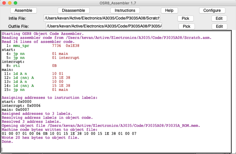
In the above screen shot, we the output of the OSR8 Assembler for our tpreg0_demo.asm demonstration program. The OSR8 Assembler will also perform dis-assembly, where we take the hexadecimal memory file and translate it into OSR8 assembly language. The Pick buttons allow us to select input and output files for the assembler. The Edit buttons opens the corresponding file in a black-and-white editor with copy, paste, save and undo key bindings. Save from the editor and press Assemble to assemble the input file and re-write the output file.
The Instruction button prints out all the instructions known to the assembler. The assembler gets its list of instructions from the OSR8 source file. We cut and paste the instruction definitions directly from the VHDL source code and into the data section of the ORS8 Assembler script. When the assembler starts up, it parses the VHDL definition and creates a list of instruction pneumonics and opcodes. If we modify the OSR8 so as to eliminate instructions or add new ones, we can re-configure our OSR8 assembler easily by over-writing the OSR8_Assembler.tcl data section with the new VHDL instruction definition list.
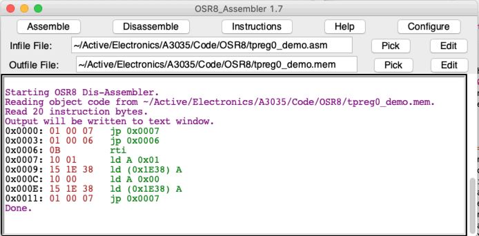
Press the Disassemble button and the tool will read in the output file and generate an assembly-language version of the object code using the instruction pneumonics. There will be no constant definitions: all constants are replaced by their actual hexadecimal values. The disassembler allows us to check that the assembler is working, or that our constant declarations are working.
[19-JAN-21] To illustrate how we can implement the OSR8 processor in a programmable logic chip, we will use the example of the A3035A application. Download OSR Demonstration archive and decompress. You will get a folder P3035 which contains all the files you need to compile the P3035A09 firmware for the A3035A assembly. Install the Lattice Diamond compiler. We built the demonstration on Lattice Diamond version 3.11.3.469. Start Lattice Diamond by double-clicking on the P3035.ldf file.
The P3035 project compiles code for the LCMXO2-1200ZE logic device in a WLCSP25 package. The P3035A_Main.vhd is the top-level source file. It defines the memory manager, interrupt handler, input-output interface, and clock generator. It uses OSR8V1R1.vhd to define the processor, and three other automatically-generated files to define the process memory, program memory, and eight-bit multiplier. The program memory is initialized from P3035A_ROM.mem, which you will find in the OSR8_Demo folder. We generate P3035A_ROM.mem with the OSR Assembler tool. Download tpreg0_demo.asm, open the assembler and use it to generate a new copy of P3035A_ROM.mem from tpreg0_demo.asm. In the Lattice Diamond project, double-click on P3035A_ROM.ipx in the File List. A window opens. Press Generate, and the compiler will take the MEM file and use it to construct a new P3035A_ROM.vhd file. You can look at the VHD file and see that it defines the contents of a 1-KByte read-only memory to be implemented in one of the LCMXO2-1200ZE's seven embedded memory blocks. Now synthesize, map, and generate the design. You will end up with a new JED file in the P3035/impl1 folder called P3035_impl1.jed. If you have not already done so, install the Lattice Diamond Programmer and with it open the impl1.xcf programmer file, which sets you up to program a P3035AV1 assembly through its programming extension. You had best have on hand such an assembly, or you won't be able to see the results of your OSR8 work. Power the A3035A with 2.7 V. Program the board and examine pin P1-1 with an oscilloscope. You should see a square wave.
Detail: When you program the device, you have to make sure the board power is on, so we like to put an ammeter in series with the power supply. But the ammeter adds a complication in that the board needs about 30 mA to power up, but its quiescent current consumption is only 100 μA. If you set the ammeter to 200 μA range, it will not deliver 30 mA. So you have to switch between 200 mA range and 200 μA range to program and monitor the device.
Assuming you have the demonstration program running, try to modify it so as to alter its square wave frequency. Add some NOP instrutions to the main loop, for example, re-assemble P3035_ROM.mem, re-generate P3035_ROM.vhd, re-compile the JED file, and re-program the A3035A. If your alterations work, you are ready to try more complicated programs. Here is the memory map provided by the P3035A09 memory manager.
| Address (hex) | Read/ Write | Function |
|---|---|---|
| 0000 | R/W | Program Variable Memory and Configuration Data (6 KB = 6144 Bytes) |
| 1700 | R/W | Bottom of Program Stack (SP = 5888) |
| 17FF | R/W | Top of Program Stack (SP = 6143) |
| 1E00 | R/W | Sensor Data Hi Byte (D0-D7 give SD8-SD15) |
| 1E01 | R/W | Sensor Data Lo Byte (D0-D7 give SD0-SD7) |
| 1E02 | W | Sensor Register Location (D0-D6 give SA0-SA6) |
| 1E04 | W | Sensor Control Register (write initiates access, D0-D2 are GYSEL, SAWR, SA16) |
| 1E10 | R | Interrupt Request Bits (D0-D7: TMR, TXD, SAD, INTG, INTA, GPI1-3) |
| 1E12 | R/W | Interrupt Mask Bits (store "1" to Dn to enable interrupt n) |
| 1E14 | W | Interrupt Reset Bits (write "1" to Dn to clear interrupt n) |
| 1E16 | W | Interrupt Set Bits (write "1" to Dn to set interrupt n) |
| 1E18 | R/W | Interrupt Timer Period (multiple of RCK period = 30.52 μs) |
| 1E19 | W | System Reset (D0 is SWRST) |
| 1E20 | W | Transmit Hi Byte (D0-D7 are TD8-TD15) |
| 1E21 | W | Transmit Lo Byte (D0-D7 are TD0-TD7) |
| 1E22 | W | Transmit Channel Offset (channel = device_id + offset) |
| 1E24 | W | Transmit Control Register (any write initiates transmission) |
| 1E30 | W | Enable Transmit Clock (D0 is ENTCK) |
| 1E32 | R | Transmit Clock Frequency (0-255, multiple of RCK = 32.768 kHz) |
| 1E34 | W | Transmit Clock Divider (0-15, divides ring oscillator to get TCK) |
| 1E36 | W | Boost CPU Clock (D0 is BOOST) |
| 1E38 | W | Test Point Register (D0-D7 are CPUTP0-CPUTP7) |
| 1E39 | W | Test Point Register (D0-D7 are CPUTP0-CPUTP7) |
| 1E3A | W | Multiplier Input A |
| 1E3B | W | Multiplier Input B |
| 1E3C | R | Multiplier Output HI |
| 1E3D | R | Multiplier Output LO |
We discuss the gyroscope and acceleromater in detail in the A3035 manual. If you want to read out the gyroscope sensor timer, transmit the timer and transmit other signals like parabolas and square waves, you can do so without configuring either sensor, as in multiplier_demo.asm. We read out the three gyroscope and accelerometer coordinates and transmit them at 128 SPS with the help of a regular interrupt in C3035AV1.asm
The A3035A has 6 KBytes of RAM. The OSR8V1 puts the bottom of its stack 256 Bytes from the end of the RAM area, at address 0x1700. If the stack pointer ever hits 0xFF, the processor will assert SPOF (stack pointer overflow). The A3035A provides 1 KByte of read-only program memory. As soon as your program exceeds 1024 bytes, as reported by the OSR8 Assembler, it won't fit in the A3035A program memory.
[11-DEC-20] For initial development of the processor for the A3035A, see its Development Page.
[03-FEB-21] We add an instruction "ld B,(nn)" and find the OSR8 increases by 10 LUTs. We remove, then add instead "ld B,A", which adds 30 LUTs.
[25-APR-21] We are working on the OSR8V2 for the LCMXO2-7000 of the A3038BB. We increase the program memory from 1 KByte to 8 KByte, increasing all code memory pointers from ten bits to thirteen bits. The total size of our P3038BB firmware drops from 1081 to 1072 LUTs as a result of this increase.
[30-APR-21] The combinatorial implementation of the interrupt set and reset signals in our P3038BB01A firmware produces erratic set and reset actions as our OSR8V2 is running a demonstration program with a periodic interrupt. We change the implementation of the set and reset signals to registered under the control of the CPU clock and they behave well. We implement the same change in the P3035A10 firmwarwe top produce the prototype P3035A11. We set IRQ0 (interrupt request zero) when the IRQ timer first reaches zero, so that we generate only one interrupt request every time the timer runs down, even though the timer runs off RCK (32.768 kHz) and the processor runs off PCK (10 MHz). With LCMXO2-7000HC-4, max PCK is 17 MHz, with -5 is 20 MHz, and with -6 is 22 MHz. We have the -5 for the A3038BB-A. Our BB01A final code fades the white LEDs in and out using a 128-Hz interrupt and a continuous main loop. It exercises the test points to show interrupt execution and the 128.000 Hz interrupt clock.
[12-MAY-21] We test "seti" and "clri" and find they work to disable and enable interrupts. We have a 6-μs pulse on a test point between "seti" and "clri". We have interrupts at roughly 2 kHz at random. We never see the pulse interrupted. The interrupts themselves execute immediately after the end of the pulse.
seti
ld A,(test_point_addr)
or A,0x04
ld (test_point_addr),A
ld A,100
dly A
ld A,(test_point_addr)
and A,0xFB
ld (test_point_addr),A
clri
[07-APR-22] The new OSRV3 provides control over its process and program memory size through generic constants, as well as the start and interrupt locations, and the stack pointer base and top. We use this more flexible version as we are developing the A3041A, where we are adjusting the memory sizes as we go. By adjusting its constants, the V3 code is backward compatible with the V2 and V1 code.
[09-APR-22] We try the OSRV3 with the A3035A code. The processor does not run. We trace the problem to the generic map in the declaration of the OSR8 entiti. Here is our attempt to make the CPU flexible through generic constants. Only by removing the generic map can we get the CPU to run. If we define two generic constants that we don't even use, and leave all other code the same, the processor won't run. For example, the addition of prog_addr_top and cpu_addr_top in the following code, two constants we never use, stops the processor from running.
[11-APR-22] Upgrade to Lattice Diamond 3.12, now find we can use generics, and identify a compiler bug in the interrupt handler. Proceed with further improvements to the OSR8V3. Delete the rst_cpu instruction, which we never implemented, and has been replaced by writing to a sofware reset register.
[12-APR-22] Add generic constants to the OSR8V3, and all goes well with the new compiler. The OSR8 may now be configured from the main unit.
[29-JUN-22] The OSR8V3 has undergon further changes in its adaptation to the A3041. We are recording development in a GitHub repositor, P3041. From VHDL comments, "Remove stack overflow flag. Stack pointer always resets to zero, so CPU must have RAM at address zero to use as initial stack during initialization. The initial stack will allow the CPU program to load the stack pointer with a new value."