 Head-Mounting Transmitter (A3040) Development and Production
© 2021-2024, Kevan Hashemi,
Open Source Instruments Inc.© 2022, Calvin Dahlberg, Open Source Instruments Inc.
| 2021 | 2022 | 2023 | 2024 |
[25-OCT-24] Chronological account of A3040 HMT development.
[19-DEC-21] Sketch of prototype here.
[03-JAN-22] Finish first draft of A304001A rigid-flex circuit board, equipped with four amplifiers. We are using the ADG804 four-to-one analog multiplexer to select one of four signals for the ADC. We are using the LTC1865L in SOP-8 package because we want to conserve our stock of MSOP-10 packages for our smaller transmitters. We find that the op-amp and passives for each amplifier weigh 34 mg.
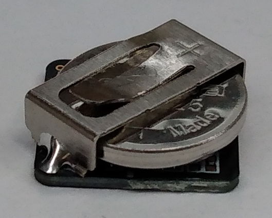
[06-JAN-22] We receive battery retainers and modify them by cutting off end flanges and solder to an existing 12.5-mm square transmitter board. The corners of the retainer protrude by 0.5 mm. We prefer to bend the retaining spring so that it pushes down on the center of the battery. After these modifications, the battery is secure in the retainer, with its negative tab pressed on the center of the circuit board, where we expect to have our gold-plated negative battery pad.
[03-FEB-22] Change pinout of our Omnetics socket connector, J1, to match the manufacturer's A78538 drawing, modify all sketches, schematic, and printed circuit board files.

[16-FEB-22] We have A304001A rigid-flex boards in panels of five. Load Omnetics connector we burn off an EIB-8 onto the footprint of J1. Trim battery holder, bend down its spring, insert CR1225. Wrap in blue, self-adhesive silicone. Mass is 2.3 g.
[28-FEB-22] Kit for 15 of A30304A on 10-day turn is ready to ship.
[16-MAR-22] We have fifteen A3040AV1 assembled circuits. We have assigned an input-only pin on the logic chip to the SCK output. We remove R7 and use the D0 tuning bit for SCK, connect the R7 pad to U3-7 with a wire link. The D0 bit is U4-G1, on Bank 0 of the logic chip, which runs on 1.8 V, so the HI level will be only 1.8 V. We program as D3: all channels enabled, 512 SPS. Active current is 231 μA, less than the 270 μA we predict with our current calculation formula.

We load a battery holder and insert CR1225 battery. Obtain robust reception in FE3A enclosure with one pick-up antenna in a few locations, no systematic test of reception. Right now, the antenna matching network is our first guess: 10 nH series inductor with 1 pF parallel capacitor.

Our nine-way Omnetics connectors with guide pin, A78538, are due to ship to us on 21-MAR-22. We touch the pads of the connector and see voltage induced in all four input channels on our Receiver Instrument display. The ADC appears to be working despite the fact that SCK is being driven by only a 1.8 V logic signal when the ADC expects 3.0-V logic.
[20-MAR-22] We clip the programming extension of our working, programmed A3040D3, No224. We wrap in silicone and trim. We are still missing J1. Mass is 2.51 g. Of this 1.10 g is the A3040AV1 assembly, 0.87 g is the CR1225 battery, and 0.54 g is the silicone wrap. When we load a CR1025 battery, the mass of the circuit without wrap is 1.76 g, the mass of the battery is 0.65 g. Apply wrap, total mass 2.30 g. Running off the CR1025, we record from all four channels and see VBAT = 3.0 V (fresh battery). We prepare two more AV1s and program as D1..D4, measuring current consumption, which we find to be linear with sample rate, 17 μA + 0.110 μ/SPS. Our A3040A02 firmware brings the transmit channel numbers and input channel numbers into agreement. If the base transmit channel number is b, the channel numbers for X1, X2, X3, and X4 inputs will be b, b + 1, b + 2, and b + 3.
[22-MAR-23] We solder silicone leads to our No224 AV1 and connect these to a 15-mVpp, 10-MΩ signal source so as to measure gain versus frequency. With 10-MΩ input resistance, we expect to see 7.5 mVpp at X1..X4. Assuming VB = 2.7 V and gain ×100 in the middle of the amplifier pass-band, we expect amplitude roughly 6.5 kcnt rms, with cut-off frequency 160 Hz, and this is indeed what we see.
[23-MAR-22] We experiment with our antenna matching network, L1 and C26 in schematic. We program an A3040AV1 to turn on its transmitter (U6) continuously. We connect an external tuning ramp 0-5 V to the TUNE input of U6. We place the antenna of the A3040AV1 near the coil antenna of an A3038DM-C detetector module in which we have replaced the 900-930 MHz bandpass filter with a wire link. We look at the logarithmic power measurement, P, on the detector module. The peak power received is a strong function of the location of the transmitter. The variations in power received are a weak function of location. We place the transmitter in a petri dish with the antenna sticking up in the air, about 10 cm from the detector antenna.
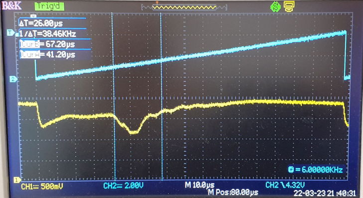
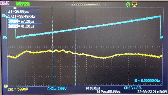
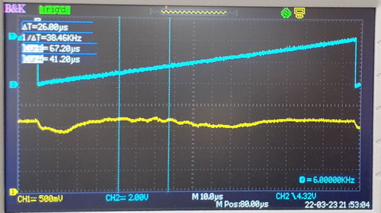
Our original tuning newtork was 10 nH with 1.0 pF. This network produces a 20 dB reduction in transmit power in the 902-930 MHz band when compared to no network at all (0 nH and 0 pF). When we increase the tuning capacitor to 2.0 pF, we see a slight increase in power emitted in our 900-930 MHz band compared to no network. We equip one A3040D3 with 10nH/2pF and another with 0nH/0pF. Both have had their programming extensions removed. We fold up and wrap in silicone. We place on a petri dish in FE2F enclosure and move around, watching reception from a single A3015C damped loop antenna connected to an Octal Data Receiver. We try different arrangements of the antenna and transmitters. In each arrangement, we have both transmitters oriented the same way and close to one another. With transmit antennas vertical, we obtain robust reception from both transmitters in ten arrangements. With antennas horizontal, we obtain robust reception from the 10nH/2pF network in 18 of 20 arrangements, and from the 0nH/0pF network in 10 of 20 arrangements. We damage No5. We load 10nH/2pF onto No224 and No1. We clip No1, fold both, and compare. We obtain robust reception in only half the arrangements, and equally for both. We try 100pF/10nH (100 pF in place of L1, 10 nH in place of C26) on No1. Reception is far inferior to No224 with 10nH/2pF. We try 100pF/0pF on No1. Reception from No1 100pF/0pF and No224 10nH/2pF robust with antennas vertical. With antennas horizontal, we see robust reception from 100pF/0pF in two thirds of arrangements, and robust reception from 10nH/2pF in only one third of locations. Load No224 with 1nF/0pF. Reception from No1 100pF/0pF and No224 1nF/0pF is equally robust with antenna horizontal.
[24-MAR-22] We receive 15 Omnetics connectors. Solder one to No1, takes about five minutes. Wrap with 40-mm tape and CR1225 battery, mass 2.6 g. The connector weighs 57 mg. We solder leads to an EIB-8 and plug our A3040D3 into the EIB-8. We connect the EIB-8 leads to a four-way SCT-BNC interface, and by this means we apply a frequency sweep to all four inputs and measure frequency response. At first, amplitude is low and varies from channel to channel. We heat up and blow dry, now obtain uniform response.
[28-MAR-22] We wrap No1 in Saran Wrap. The wrap does not stick to itself well enough to provide a lasting seal, but mass with three layers of Saran Wrap is 2.1 g. Some residual wrap material adheres to the tubes of socket J1.
[30-MAR-22] We have five A3040D3 ready to ship to UCL. Frequency response D1_1.gif. We ship with ten CR1225, ten CR1025 batteries, and one meter of silicone wrapping tape. Calibration constants below.
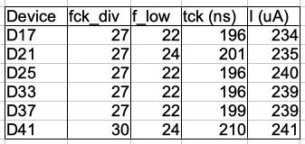
During calibration, we measure transmit spectrum of several devices before and after we replace the A3040AV1's 10nH/1pF antenna matching network with 1nF/0pF. In all cases, we first perform the SCK/R7 modification. The transmit center frequency is stable to ±1 MHz, and power stable to ±3 dB as we change the matching network and re-measure the spectrum.
The prototype A3040A provides a nine-way, dual-row, 0.025" pitch, surface-mount socket with a single guide post for connection to the electrode interface board (EIB-8). We use custom Omnetics NSD-09-VV-G, which we order with part number A78538-001.
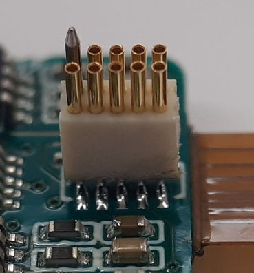
We use the pin numbering given by the manufacturer. The figure below is an exerpt from the S3040A_1 schematic, showing pin numbering as seen looking down on a soldered socket. We add pin "G" for "guide post" so that we have a label for the tenth pad on the printed circuit board. This pad is not used by the connetor, because there is no connection pin below the guide post.
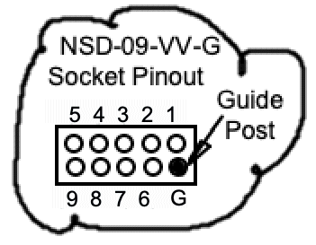
The NSD-09-VV-G socket mates with any NSD-09-G plug, provided the plug's guide post hole is in the G position. We designed the A3040A to mate with Neualynx's EIB-8 electrode interface board. In this figure, we see the top of the EIB-8's nine-way plug, with the guide post hole in position G on the top-right. The EIB-8 provides ten connection pads. With J1 on the A3040AV1 circuit loaded in its original (0°) orientation, the two GND pads on the EIB-8 will connect to VC, the reference voltage of the four amplifiers. The other pads connect as shown below. We also show how the pads on the EIB-8 will connect to the circuit if we reverse J1 on the A3040AV1 footprint. In the original orientation, the A3040AV1 antenna extends to the right of the figure. In the alternate (180°) orientation, the antenna extends to the left. The latter orientation turns out to be the one that we prefer, because the EIB-8 is designed to have the GND pads towards the nose of our host animal.

Within the HMT circuit, we refer to the reference potential as "VC", the "common voltage". Once we connect this potential to an animal body, we say it is "grounded". Our assumption is the the GND pads on the EIB-8 will be used for a low-impedance connection to the animal body.
[08-APR-22] We wrap an HMT in plumber's teflon tape, and are well-satisfied with the result. Mass with CR1225 battery is only 2.2 g.
[11-APR-22] We receive this picture from ION of an A3040D3 wrapped in British clingfilm.
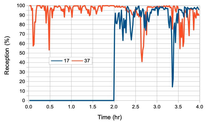
[05-MAY-22] We have four hours of recording from ION of No17 and No37 mounted on mice. In the first hour we nave No37 running. In the second hour we have No17 and No37 running.
We must epoxy the PZN-08-VV connector to the HMT or else it can rip off the circuit board while we are trying to remove the HMT from its EIF.
[06-MAY-22] We receive another six hours of recording from the IVC rack at ION. There are half a dozen A3028C transmitters running along with two A3040D3 HMTs. We measure reception from HMT channels No17 and No37, and compare to SCT channels 201, 203, 205, and 210.
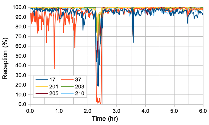
Reception from all transmitters drops dramatically from 2.2-2.5 hr. We assume the enclosure door was opened for access. From time 2.5-6.0 hr, reception from each channel is as follows.
Channel   17   37   201  203  205  210
Average 95.2 97.6  99.4 99.1 99.2 97.0
In the period 0.0-2.2 hr, reception from the two HMTs is inferior to reception from the SCTs. After 2.5 hr, reception from HMTs is slightly inferior on average (97% compared to 99%). When we implant an SCT, the presence of water around the device slows down the electric waves propagating back and forth along the antenna. We find that antennas of thirty to forty millimeters are ideal for subcutaneous operation. The HMT antenna is operating in air, where the resonant length of a straight quarter-wave antenna is 80 mm. The HMT antenna is straight, but it is only 14 mm long. The antenna conductor is 80 mm of zig-zag track, but this zig-zag does not behave the same as a straight wire. It was our hope that the 14-mm zig-zag antenna would work fine without any matching network at its base. But it now appears that we are going to have to spend a few days figuring out what inductor and capacitor value we should load for L1 and C26 in order to get the antenna to resonate.
[17-MAY-22] Our collaborators request that we reduce the distance between the mouse's head and the HMT circuit. We cannot modify the existing Omnetics connector, but we order a selection of 0.4-mm and 0.35-mm pitch board-to-board connectors that will reduce the separation to less than 2 mm.
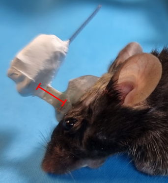
[20-MAY-22] Two A3040D3 have failed when the socket on the HMT broke off at the solder joints. The connector on the EIB is glued in place. Our collaborators do the same for the connectors on their HMTs. They use UV curing epoxy.
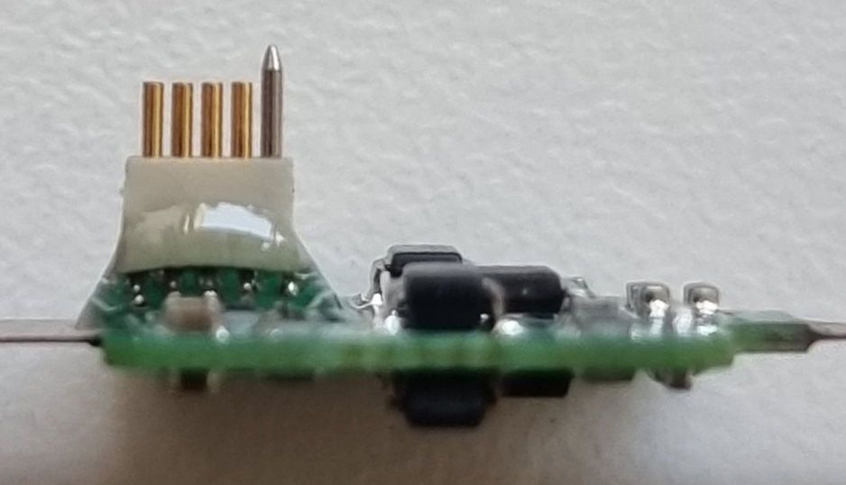
[25-MAY-22] We try alternatives to the 9-Way Omnetics connector. We have a 6-Way 0.35-mm pitch 5861-series board-to-board plug and socket from Kyocera and a similar plug and socket from Molex in their Slimstack series. We glue these new connectors to circuit boards so that we can press them together and pull them apart.
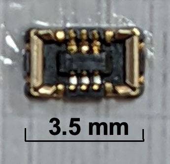
The separation of the circuit boards is less than a millimeter. It is difficult to get the plug and socket to mate when we cannot see either connector. We would need two alignment pins on the electrode interface board to align the HMT with the connector when mounting on the animal.

The connection force provided by these new connectors is of order 0.1 N compared to 3 N provided by the Omnetics connector. If we add threaded ends to our two alignment pins, these could pass through holes in both layers of the HMT circuit. But the pins would eventually encounter the battery an be unable to emerge from the HMT. If we separate the pins sufficiently to avoid the battery, the electrode interface board will have to be 14 mm long. Even if we figure out how to get the pins past the battery, we still have to figure out how and when to wrap the circuit in teflon.
[26-MAY-22] Our collaborators inform us that the orientation of J1 on the A3040A is incorrect for use with the EIB-8. The orientation we chose places the hole in the EIB-8 at the front end of the mouse's head, rather than at the back end. We now consider what will happen if we rotate J1 with respect to its original orientation. We refer to the EIB-8 manual for the conections between its pads and its Omnetics plug.
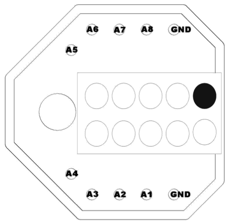
In the following table, we map out how the A3040AV1 circuit's four inputs and ground connections will be mapped to the EIB-8 if we rotate J1 on its footprint.
| Connector Orientation |
Footprint Pin |
Connector Pin |
EIB-8 Pad |
Electrical Function |
|---|---|---|---|---|
| 0° | 1 | 1 | GND | GND |
| 0° | 2 | 2 | A1 | X2 |
| 0° | 3 | 3 | A2 | NC |
| 0° | 4 | 4 | A3 | X4 |
| 0° | 5 | 5 | A4 | NC |
| 0° | 6 | 6 | A8 | X3 |
| 0° | 7 | 7 | A7 | NC |
| 0° | 8 | 8 | A6 | X1 |
| 0° | 9 | 9 | A5 | NC |
| 0° | G | G | GND | GND |
| 180° | 1 | 9 | A5 | GND |
| 180° | 2 | 8 | A6 | X2 |
| 180° | 3 | 7 | A7 | NC |
| 180° | 4 | 6 | A8 | X4 |
| 180° | 5 | G | GND | NC |
| 180° | 6 | 4 | A3 | X3 |
| 180° | 7 | 3 | A2 | NC |
| 180° | 8 | 2 | A1 | X1 |
| 180° | 9 | 1 | GND | NC |
| 180° | G | 5 | A4 | GND |
If we rotate the connector on the A3040AV1, we will have the EIB-8 pads connected to the A3040AV1 circuit in the following manner: A5=GND, A1=X1, A3=X3, A6=X2, and A8=X4, see diagram.
[19-JUN-22] We complete a study of how we might fasten the HMT to an animal's head with magnets, while making the electrode connection with a smaller, lower-profile connector.

Calvin makes the following comments, "smaller connector tends to rock back and forth. Aligning magnets works so-so. Smaller connector may be shorter than other components on the board. Magnets are hard to work with, although hot glue works okay. Two and three magnets on both sides would definitely go over 1g weight limit." The rocking of the two boards with respect to one another, while the plug and socket rotate, is of particular concern to us: we may see movement artifact introduced into our EEG. The additional weight is the greatest cost.
[11-JAN-23] We are working on a new electrode interface fixture (EIF). We abandon the NSD/NPD connector in favor of a new design by the same manufacturer, Omnetics Corporation. The PZN connector is a hermaphroditic, intrinsically-polarized connector. We issue a new version of the schematic, S3040B_1, in which we use the manufacturer's pin numbering for the PZN-08-VV on the HMT. In the EIF, we modify the pin numbering to match the HMT, and use the same connector but with through-hole pins, PZN-08-DD.
[12-JAN-23] Study D1.17 returned last summer from ION. Consumes 150 mA from external power supply. Replace MAX2623, U6, and now it works fine. We re-tune by loading 1 kΩ in parallel with R3. Current consumption 245 μA, we leave it running with a battery. We are applying modifications to six more circuits. We D41 in fine shape. We have a prototype D242 that may be fine. We have D33 for antenna tuning only. We have another board that is scrap for spare parts. Our objective is to prepare 4 for shipping with the PZN-08-VV connector.
[13-JAN-23] We prepare an EIF prototype with five 0.5-mm diameter leads soldered to its pins. The 0.5-mm diameter leads are far more flexible than our 0.7-mm leads, and the spring itself is smaller, so it takes up less space in a lap solder joint like those shown below. We experimented with sliding the 0.7-mm lead's spring over the connector pins and soldering, but we find we must twist the spring onto the pin, which can weaken the pin.
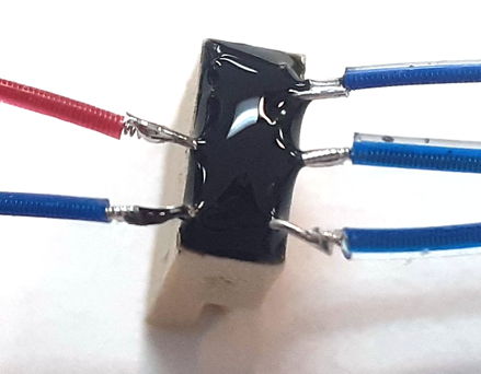
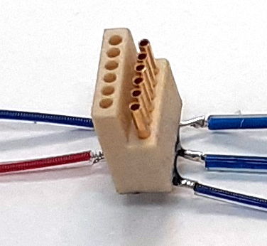
We apply a little black DP270 encapsulation epoxy to the bottom of the connector to reinforce the bends in the leads.
[19-JAN-23] The black epoxy did not adhere well to the leads shown above, but instead collected elsewhere. We continue making prototypes, trying to get the pins and joints smaller and shorter. We assemble the following with five leads, then apply epoxy. With the bottom facing up, the black DP270 creeps off the solder joints and starts making its way down the outer walls of the connector. So we flip the connector right way up, supporting it over an aperture with a weight on its leads. The result, photographed the next day, shown on the right belwo.
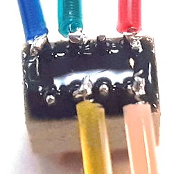
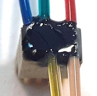
There are several metal points and one solder surface where the epoxy covering is so thin as to be transparent. In our experience, coatings this thin break off or wear through quickly. We will try rotating the EIF while the epoxy is curing, as we do with SCTs, so as to neutralize gravity and leave the epoxy distribution to be dominated by surface tension.
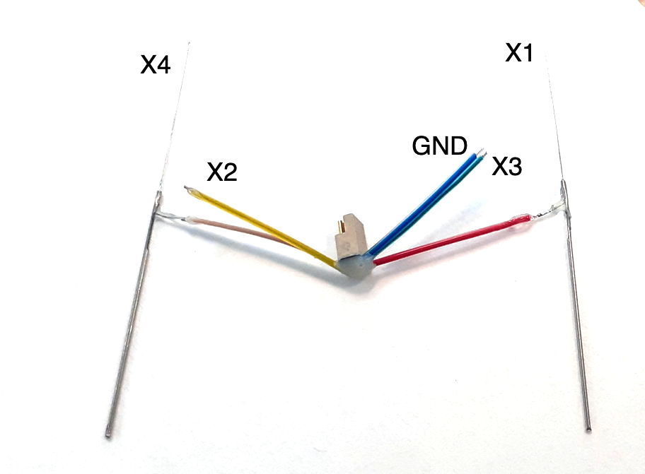
[20-JAN-23] We solder two X-Electrodes to our latest prototype, producing the EIF8-XAAX shown below. We construct four clips with magnets that mount on our rotation
[30-JAN-23] We have 5 of A3040A3 with PZN-08-AA loaded. Current consumption is 235-246 μA.
[08-FEB-23] By loading 27 nH for L1 and 0.2 pF for C26 we find that antenna output power increases by a factor of ten. Full report to follow. Reception in air in Faraday canopy with four pick-up antennas is 98%. We receive PZN-08-DD, connector with wire contacts, shown below.
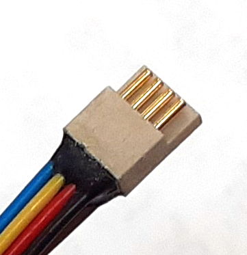
Consulting our connector pinout, we construct the following table of colors, pin numbers, and functions.
| Pin | Color | Function |
|---|---|---|
| 1 | brown | GND |
| 2 | black | GND |
| 3 | orange | X3 |
| 4 | red | X2 |
| 5 | green | none |
| 6 | yellow | none |
| 7 | purple | X1 |
| 8 | blue | X4 |
We record frequency response of our five A3040D3, all twenty channels, see D1_17.gif. When one device fails, we examine the circuit and note a missing capacitor. We load the capacitor, wash, dry, and test again: it passes.
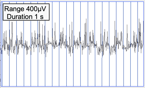
[13-FEB-23] We have 8 of EIF8-XAAX ready to ship. We have four A3040D3 ready to ship. A fifth shows low gain in one channel. While performing quality control we discover a problem with the digitization. When we apply a 15-mVpp sinusoid to X1, we see 400 μVpp crosstalk in X2. When we apply the sinusoid to X2 we see the crosstalk in X3, X3 talks to X4, and X4 talks to X1.
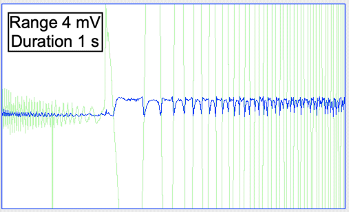
Examination of the firmware reveals that we are changing the analog multiplexer address lines (A1 and A0 in the schematic) on the rising edge of ACTIVE, which is only 10 μs before we initiate conversion in our ADC. In the four-channel A3047, we don't see this crosstalk. In that firmware, we are changing the address on the rising edge of End Clock (ECK), which is at least 70 μs before conversion. We correct our P3040 firmware, starting a new version P3040A03.abl, in which we change the address on the rising edge of ECK. The feedthrough crosstalk disappears.
[15-FEB-23] We increase the output power of the A3040D3 by a factor of twenty with a new antenna matching network. We try several inductors in place of L1 and vary the capacitor we load for C26 until we arrive at 27 nH and 0.2 pF as the most effective network.
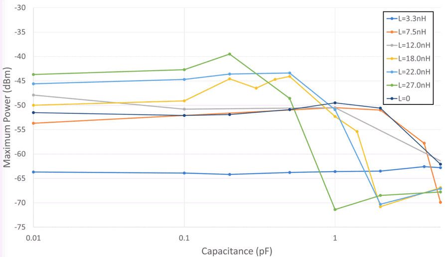
To measure relative power, we place the HMT, folded over with battery loaded, in the same orientation on a petri dish in an FE3A 20 cm from an A3015C loop antenna connected to an A3008 spectrometer. We used the peak power of the spectrum as our measurement. Peak power is 13 dB higher with the new network than with our 0 nH and 0 pF.
[24-FEB-23] We test JBWeld structural epoxy for circuit corrosion by applying it to a circuit board then poaching at 60°C for a week. We see no sign of corrosion. The glue is non-conducting and water-proof. Our DP270 epoxy has been crawling all over our PZN-08-DD connector but failing to secure the leads and pins. The JBWeld is more viscous, and we obtain the superb result shown below.
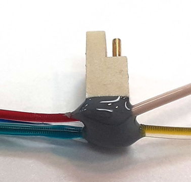
The epoxy has wicked into the lead coils and around the joints. But it has not progressed around the connector. To obtain the above result, we held the connector in our rotator while the epoxy cured. We obtain almost exactly the same result with DP460-NS (the no-sag version of DP460).
[27-FEB-23] We have poached DP460, clear DP270, JPWeld, and dental cement on four circuits for a week. We see no sign of adhesive-induced corrosion in any of the samples. We are satisfied that any of these may be used for our electrode interface fixtures. We complete layout A304001B with modificaionts listed. The board is made for the PZN-08-VV connector, corrects an error in the original layout, adds a 0V pad to the programming extension and a signal ground pad near the analog switch.
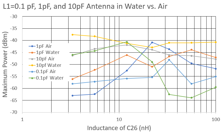
[08-MAR-23] We measure power emitted by the HMT antenna when it is immersed in water to within a millimeter of its base. The HMT body remains out of water, but folded over in its usual fasion. With the antenna in water, we see more power with an inductor from the antenna base to 0V. So we try various values of base inductor and series capacitance. We compare power emitted in air and water for each matching network.
[14-APR-23] Settle on the A3040BV1 bill of materials: we will give all four amplifiers frequency response 0.3-80 Hz. We are shipping A304001BR1 circuit boards and kit to NPi Technologies today.
[02-MAY-23] We receive 45 of A3040BV1 assemblies. Update firmware and program for D2, four channels 256 SPS. Current consumption is 139 μA compared to our expected 148 μA. We load the PZN-08-VV connector, but we do not epoxy. We cut flanges off the battery clip and load. We connect the ground pad on the programming extension to P1-7, because the pad ground connection is missing on the A304001BR1. We apply 10-MΩ sweep to all inputs and see a nice 0.3-80 Hz response. We are now able to increase the center frequency of the transmission in steps of one 5-bit dac count. The A3040A allowed only steps of two because of the way we corrected a layout error.
[12-MAY-23] We are learning how best to load the PZN-08-AA onto our A3040BV1 assemblies. While programming and testing A3040B1 we are struck by the power of the emitted radio frequency signal, and the extent of our operating range. We forgot to remove the battery from one HMT, placed it in our library five meters away, and still obtained better than 80% reception on our desk.
[09-JUN-23] We have 34 of A3040D2 ready to ship. We lost one circuit because we glued the connector before performing QC1, and one contact was faulty. Other than that our yield was 100%.
[28-AUG-23] We have five of A78914. These are PZN-08-WC with teflon-insulated, stranded, stainless-steel wires loaded (wires are A-M Systems 793200). We hope to use these connectors as a starting point for the assembly of electrode interface baords.
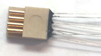
[30-AUG-23] We receive quotation from Omnetics Corporation for PZN-08-WC with A-M Systems 78600 teflon-insulated solid silver wires loaded, part number A78967, $72 each, 12 weeks.
[31-AUG-23] At UCL our collaborators have deployed two HMTs with EIF8-XAAX head fixtures. They report, "The recordings from one surgery were exceptional, with a spontaneous seizure recorded in unprecedented detail. Changing batteries equally has thus far been successful and we have been able to record of over a month. We have however run into a problem with the Omnetics 8 pin Nano connector working itself loose due to animal activity. Three times the mouse has been able to completely remove the HMT in the days following connection, resulting in a minor mauling of the transmitter by the mouse. Thus far the transmitters have resisted destruction, but some damage to the antenna can be seen."
[08-SEP-23] Mouse removed HMT and chewed through antenna completely. Collaborators having some success with Kwik-Cast to hold the connectors together. They also note that it is the mouse pulling on the wrapper with its claws that allows the mouse to pull off the HMT. They have not been using plumbers tape, but rather some stronger tape. They try clingfilm and the mouse tears the clingfilm but fails to remove the HMT.
[29-SEP-23] Working on P3040B firmware. We try uniform sampling by adding a conversion at the end of each sample interval, in addition to the scattered conversion during transmission. Current consumption of the A3040D2 increases from 132 μA to 148 μA as the LT1865L makes the extra conversion. We don't think the benefit of uniform sampling in the HMT is worth the 10% decrease in battery life. In the A3049, which uses the ADS8860, the increase is negligible.
We prepare firmware for the A3040C2. We use a PZN-08-WD wired connector to deliver ground and signals to the device. Wires are black GND, purple X1, blue X4, orange X3, red X2. We program No69. We connect 20 mVpp to X1 and see 6.5 mV rms on W, 12 μV on X, and 8 μV on Y. The Z-channel is disabled. With 20 mVpp on X4 we see 10 μV on W, 6.5 mV rms on X, and 9 μV on Y. With 20 mVpp on X2 we see 8 μV rms on W, 6.5 mV on X, and 10 μV on Y. In this latter case, we look at the spectrum of W and Y and see sharp peak at 10 Hz, amplitude 10 μV. Crosstalk is roughly −56 dB. Current consumption 189 μA. We program No21 with the same and see 182 μA. Using 25 + 0.12 × SPS we get 179 μA.
[02-OCT-23] We adjust A3034C2 so it provides three channels at 512 SPS. Reprogram No21 and No69. Current increases from 182 μA to 196 μA and from 189 μA to 209 μA respectively. Operating life drops from 10.5 days to 9.6 days. Using 25 + 0.12 × SPS we get 209 μA.
[03-OCT-23] We prepare two A3040D3Z using two of the original A3040AV1 circuits with PZN-08-VV connectors loaded. We replace C6, C11, C16, and C21 with 50 kΩ and C7, C12, C17, C22 with 620 kΩ.
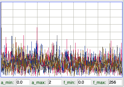
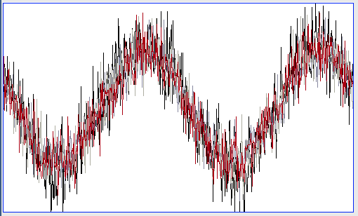
[10-OCT-23] Our A3040D3Z are noisy. We update P3040A with the code present in P3040B that reduces sampling noise. Gain of amplifiers is ×10, dynamic range 300 mV, noise 20 μV rms on all channels, spectrum below.
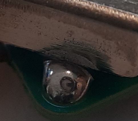
[14-DEC-23] We have three HMTs back from ION. On device 0x6170 one joint on the BC-2009 battery clip failed, see below. In future, we must make sure we solder both sides of the clip. In this case, the nickel plating on the clip peeled off.
Devices 0x74D0 and 0x552F draw over 100 mA. We replace U6, MAX2623 and current consumption returns to normal. Diagnosis: static damage to U6, which we have observed and even caused deliberately with a plasma ball in our A3048 and A3049 circuits. Solution: encapsulate U6 and antenna network in epoxy. We check gain versus frequency and find 0xFF2F and 0x6710 are perfect, but channels No70 and No72 on 0x74D0 are −6dB at all frequencies for 10-MΩ sweep, but correct gain for 100-kΩ sweep. We place in the oven to bake. After twenty minutes, remove and frequency response is correct for 10-MΩ sweep.
[11-MAR-24] We are modifying and enhancing 15 of A3040D2 to make A3040D3. We fix some ommissions in the firmware, whereby several inputs were left with pull-up resistors. Current at 2048 SPS is 220 μA for two circuits, 50 μA below our calculation.
[12-MAR-24] We are using A3040B03 firmware, which makes use of the versatile state machine introduced for the A3047. Noise with 10 MΩ source impedance is 15 cnt rms. In our A3040D3 with gain ×100, that's 6 μV.
[13-MAR-24] We note that the X3 signal is noisier than the others. We have X1 and X2 of A3040D3 around 10 μV rms when open circuit, while X3 is 30 μV. When we connect 10 MΩ 0-V source, X1 and X2 drop to 6 μV, while X3 drops to 8 μV rms. We note that digital signals A0 and A1 pass near the input of X3.
[15-MAR-24] We have 19 of A3040D3, of which 17 pass through QC1. We are now readying to apply SS5001 clear silicone to the VCO right-side pins and matching network on 6 of the 17 that passed. We already have epoxy on 2 of them.
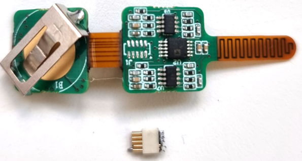
[08-MAY-24] We assemble seven A3040D3Z. These have gain ×10 and response 0.0-160 Hz. Dynamic range 300 mV. Modification to existing A3040BV1 circuits, which are 0.2-80 Hz, are arduous. We show what they look like on the bottom side here. We end up with satisfactory sweep response from all units.
[15-MAY-24] We receive twelve hours of recording from A3040D3Z and EIF8-SSSS at University of Manchester. In first hour, all four channels drift up by 7 mV, with occasional baseline shifts of the same order and time constant half a second. In the remaining hours, all four channels are stable to ±1 mV with baseline shifts of no more than 100 μV over one second. We are so surprized at the lack of DC offset in the recordings taht we ask Kate Hills to send us a photograph of the bottom side of the HMTs so we can confirm that they match this photo, and indeed they do.
[17-SEP-23] We program an A3040BV1 as A3040C2, a three-channel version with 256 SPS on each channel. The total sample rate is not an even power of two, so we are looking for synchronous noise at some frequency such as 64 Hz, 128 Hz, and so on. But we find no trace of such noise. Total noise is 4 μV in all three input channels, no switching noise, no synchronous noise. We apply 20 mVpp sinusoidal sweep to X3 and look at the sinusoidal amplitude of the same frequency that arises on X1 and X2 by cross-talk. See Crosstalk_C2 for plot. Crosstalk is −46 dB and −52 dB for X1 and X2 respectively.
[19-SEP-24] We received back from UCL in the past two weeks a total of five damaged HMTs. Four had been chewed through the flex connector. The fifth had its battery clip detached, and some other damage to the antenna network that we did not diagnose in detail.
[02-OCT-24] Re-name schematics to match the assembly runs. Add BV2 assembly, a DC transmitter that provides 0.0-160 Hz, 120 mV on all four channels. To convert to AC, we replace capacitors C6, C11, C16, and C21 with 100 nF. There is no need to set C7, C12, C17, or C22 back to capacitors because the BV2 amplifiers use the OPA2369 with its maximum offset voltage of 0.25 mV, which is negligible even in our smallest dynamic range of 30 mV. The gain-bandwidth product of the OPA2369 is 12 kHz. With gain set to ×5 in each of the two amplifier stages, we can achieve a bandwidth of 2.4 kHz. To increase the gain of the amplifier to ×100, we replace the resistors R9, R16, R23, and R30 with 100 kΩ. Now the gain of the first stage is ×20 and that of the second is ×5, making ×100. The maximum bandwidth is now limited by the first stage to 600 Hz.
[25-OCT-24] We have 50 of A3040BV2 from PCB Prime's shop in Texas. These are built for A3040D2Z, four-channel, 0.0-160 Hz, 120 mV. Program the four, current consumption 213-216 μA for three, which is significantly less than our maximum 271 μA, and 450 μA for the fourth, which must be faulty. We place with batteries in our Faraday enclosure with inputs open-circuit. In both, X1 is the quietest of the three channels (25 cnt) and X3 is the noisiest (100 cnt). We connect 100-kΩ source and noise drops to 20 cnt rms for all channels. Sweep is correct in two of them, see A3040BV2_Sweep, but one channel in the third has gain 6 dB too low.
[28-OCT-24] We have eight perfect HMTs. We had to fix several errors in our soldering of the connectors. Cutting the connector pins so they fit entirely on the pads turns out to be a mistake. Cutting bends the leads slightly, spoiling the alignment of the connector. The pins protrude slightly from the pads, but this ends up making it easier to see when the connector is aligned correctly. We replaced two OPA2369 in two faulty amplifiers, and the replacement fixed both amplifiers.
[31-OCT-24] Complete first draft of A304001C printed circuit board. We have added R37, marked OMIT on the S3040CV1_1 schematic, which we can use, in combination with omitting C17 and C21 to commandeer the X4 input as X3−. This enhancement will allow the HMT to act as a two-channel EEG with one-channel EMG, ECG, or EGG. See A304001C_Top for location of R37. We make sure that the negative battery tab is masked from solder past, as well as the PZN-08-VV footprint. But we do not mask the positive terminals of the battery, to which we will solder the clip.
[07-NOV-24] Measuring noise and recording frequency response of a batch of eighteen A3040D3Z programmed with B03 firmware. These circuits are equipped with low-offset, rail-to-rail OPA2369 op-amps. Their amplifiers have gain ×25. Dynamic range is 120 mV. In one transmitter, we observe noise of 13 counts in X1 and 42 counts in X2. We take out an older A3040D3 with gain ×100, ID=0x4462, equipped with OPA2349 op-amps. Noise is 20 cnt rms in all channels. We create B04 firmware. We play around with sample timing. If we add a uniform sample, current consumption goes up from 220 μA to 250 μA. We vary xck_offset, which was originally 7, and find that 6 produces more uniform and lower noise at 40 cnts rms. We introduce a linear shift register to generate the transmission scatter, and we are well-satisfied with its performance. We settle upon firmwarwe B04. The resulting noise spectrum is white 0-256 Hz, see below.

Previous versions of the A3040D3Z provided dynamic range 300 mV and input noise 20 cnts × 4.6 μV/cnt = 90 μV rms. These new versions we were hoping would show noise of 20 cnts × 1.8 μV/cnt = 36 μV/cnt. As it is, we are seeing 33-56 μV rms depending upon the transmitter and input, in the 0-160 Hz band. If we drop to 0-80 Hz, noise is 25-40 μV. Cross-talk with 60-mVpp input is less than −50 dB.
[20-NOV-24] We have the A304001C layout complete. We disconnect J1-2 from VC so that we can tolerate a solder joint on the EIF that connects pins 2 and 4. We R37 to allow X4 to be connected into the X3 amplifier, so X4 can be used as a reference potential for a differential EMG input.
[25-NOV-24] We take out an A3040BV2 as supplied from assembly house and program as 4 channel 512 SPS. We power with CR927 battery. We apply a 100-μVpp, 2-Hz sinusoid to all inputs.

When we turn off the sinusoid, we an average of 37 cnt rms noise on the four channels, which is 67 μV. When limited to 1-160 Hz, noise is 59, 46, 53, and 59 μV rms in the four channels. In 1-80 Hz, noise is 42, 31, 36, and 41 μV rms. We power with CR2032 and noise in 1-160 Hz is 72, 49, 56, and 63 μVrms. We take out another A2030BV2, one without a connector, program, and examine the analog signals. We see all four amplifier outputs jumping every time the analog switch selects a new channel, regardless of whether the amplifier is involved in the selection. The jump on the output of the switch is always positive. The switch is a MAX4734EUB+. We designed the circuit originally for the ADG804, which we see in the AV1 BOM. All existing versions of the A3047 use the DG2034E. We load DG2034 for U2 on our BV2. Pulses on amplifier outputs now change direction and are smaller. Noise is 56, 8.5, 15, and 10 cnts rms on X1-X4. We load J1 and connect to our 100-kΩ source. Noise is 13, 8, 8, and 8 cnt rms. We define BV3 as BV2 but with DG2034E for U2.
The charge injection of the DG2034E is only −2 pC, while that of the MAX4734EU is 60 pC and that of the ADG804 is 28 pF. The DG2034E data sheet says, "The ultra low capacitance and charge injection of the switch make it an ideal solution for data acquisition and sample and hold applications, where low glitch and fast settling are required." We agree. Noise in 1-160 Hz is now 17, 10, 12, and 12 μV. Spectrum is white.