| Description |
| Ordering |
| Versions |
| Connector |
| Analog Inputs |
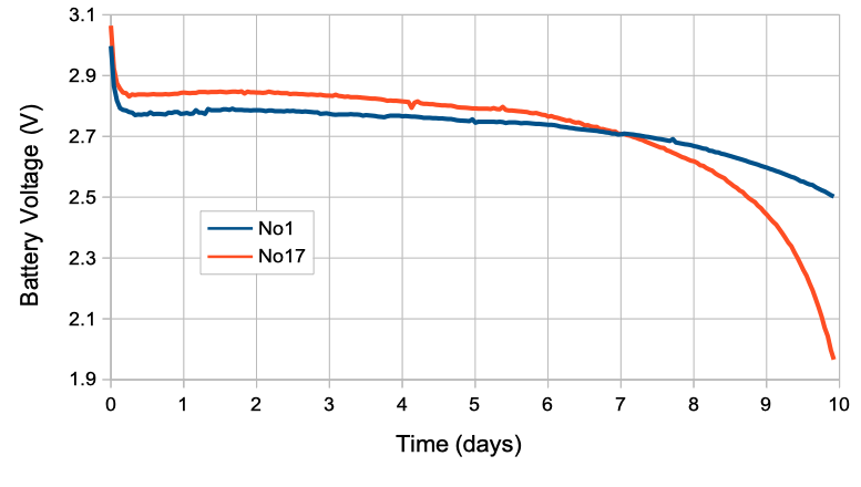
| Battery Life |
| Surgery |
| Wrapping |
| Mount and Unmount |
| Antenna |
| Warranty |
| Design and Development |
Warning: The radio-frequency oscillator on the A3040 circuit is vulnerable to electrostatic discharge. Refrain from carrying bare circuits around in your hands while wearing insulated shoes, wool sweaters, or any other static-generating item of clothing.
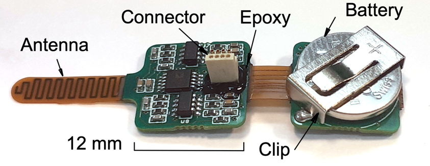
[06-JAN-26] The Head-Mounting Transmitter (HMT, A3040) is a telemetry sensor that connects to an Electrode Interface Fixture (EIF) cemented to the skull of a mouse. The A3040 provides high-fidelity amplification and recording of four biopotentials. It is powered by a coin cell that we can replace by hand. The EIF provides electrode leads and a mounting connector. The HMT transmits its wireless signals using a flat, flexible antenna that hovers over the mouse's back. All HMTs use the same telemetry system as our Subcutaneous Transmitters (SCT). A pair of identical HMTs makes it possible for us to record indefinitely from a single, freely-moving mouse. Before one HMT exhausts its battery, we replace it with the other. Because the two HMTs are identical, the telemetry channels associated with the animal are continuous. The only disadvantage of the HMT as compared to the SCT is that an animal equipped with an HMT must be single-housed, or else its companions will pull off and destroy its HMT with such frequency as to make continuous recording impractical.
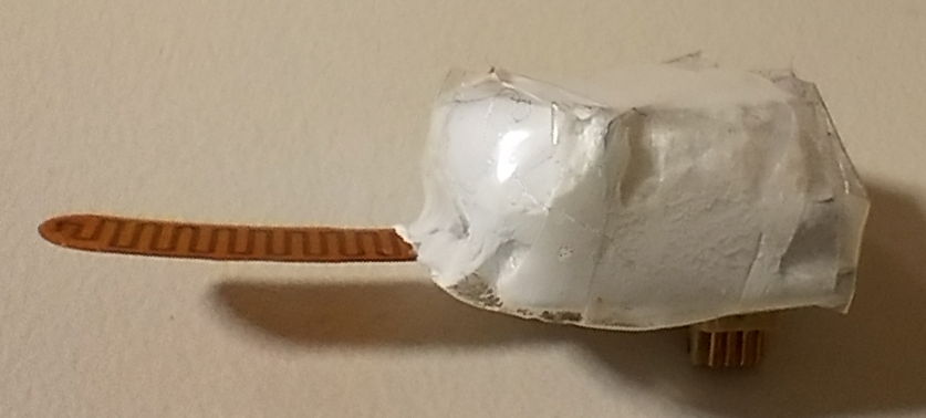
The HMT needs to be splash-proof and dirt-resistant, but it does not need to be water-proof or corrosion-resistant. We wrap the circuit in teflon tape, so as to protect the electronics from debris and water. We add a final layer of transparent tape to protect the teflon from scratching. When we deploy an HMT, we hold the host animal securely, press the HMT's connector onto the EIF, and secure the two connectors together with a drop of silicone sealant such as KwikCast. The sealant makes it harder, but not impossible, for the animal to remove the HMT. A determined host animal will still be able to remove the HMT, after which it will most likely chew and destroy the HMT. If we use a stronger adhesive, so as to guarantee that the animal cannot remove the HMT, we also make it impossible for ourselves to remove the HMT without injuring the animal, and we must be able to remove and replace the HMT in order to continue our long-term recording.
When we remove an HMT, we hold the animal securely, peel off the sealant with forceps, and work the two connectors apart. Once the HMT is detached, we immediately load another HMT with the same telemetry channel numbers and amplifier configuration onto the EIF, secure with silicone sealant, and restore the animal to its habitat. We take the original HMT away, unwrap it, clean it, dry it, and set it aside, ready to act as the next replacement. By this means, a pair of HMTs will provide continuous recordings of indefinite length on the same telemetry channels, so long as we can tolerate five-minute interruptions for replacement.
| Property | Value |
|---|---|
| Volume of Transmitter Body | 1.6 ml |
| Mass of Transmitter Body with Teflon Wrap | 2.2 g |
| Body Dimensions | 14 mm × 14 mm × 8 mm |
| Total Height with Connector | 11 mm |
| Maximum Operating Current | 235 μA |
| Battery Type | CR1225 Coin Cell |
| Battery Capacity | 2000 μA-days |
| On-Off Switch | load or remove battery |
| Number of Inputs | 4 |
| Input Impedance | 10 MΩ || 2 pF |
| Sample Rate (Each Input) | 256 SPS |
| Sample Resolution | 16-bit |
| Input Dynamic Range | 30 mV |
| Input Bandwidth | 0.3-80 Hz |
| Input Noise | ≤8 μV rms |
| Total Harmonic Distortion | <0.1% |
| Absolute Maximum Input Voltage | ±5 V |
| Minimum Operating Life | 14 days |
The A3040 has no on-off switch. Store A3040 HMTs without batteries loaded in order to make sure there is no possibility of damaging them by touching them with conducting objects. If you do leave an HMT on the shelf with a battery loaded, remove and replace that battery before you re-deploy the device. When we slide a battery into the retainer on the A3040, the device starts transmitting immediately. It keeps transmitting until the battery runs down.
The A3040 provides four amplifiers with a common reference potential. It can record EEG from one to four locations on the brain, sharing a common reference potential over the cerabellum. The A3040C-series devices provide an independent EMG input with its own reference potential, as well as two EEG inputs with a shared reference potential. These devices allow us to record two EEG signals and one EMG signal at the same time. Any A3040 input can be configured for either AC or DC amplification. The AC versions include a high-pass filter with corner frequency 0.2 H Hz. The DC versions have no high-pass filter and record all the way down to 0.0 Hz.
Our Telemetry System supports channel numbers 0-255. We ship SCTs with channel numbers in the range 1-222. By default, we will ship HMTs with channel numbers in the range 225-254. Keeping the SCT and HMT channels separate makes it easier for groups to manage their SCT and HMT experiments. An series of HMT experiments will occupy the same channel numbers indefinitely. Even as HMTs are destroyed by animals and replaced, they replacements will continue the same channel numbers. Thus HMT users will tend to make permanent reservations of channel numbers, while SCT users are moving through their set of channel numbers as old SCTs exhaust their at the end of a recording and new recordings in new animals begin with new SCTs.
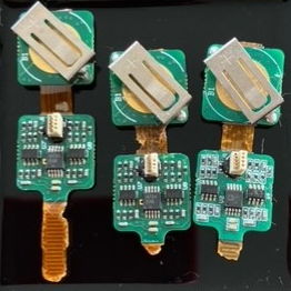
[06-JAN-25] There are many possible configurations of the HMT. We list likely and popular configurations in our version table below. The minimum order quantity for any particular version is ten pieces, unless we have that particular version ready-assembled on the shelf. If we have what you want on the shelf, we will sell you one or more at the ten-piece price. We recommend that you purchase your first set of HMTs in identical pairs. A batch of twenty HMTs, for examnple, would consist of ten pairs, and permit you to record continuously from ten animals. Each pair of HMTs shares the same channel numbers, sample rate, passband, and gain. While one HMT is recording, its partner sits idle on the shelf, ready to receive a fresh battery and wrapping. When you exchange HMTs, you remove one and load the other in less than a minute. If one of your animals pulls off and destroys its HMT, you load its partner and order a replacement immediately. We will try to ship the replacement within a week.
[09-SEP-25] All versions of the A3040 have the same profile: 14 mm × 14 mm × 8 mm with 14-mm rear flex antenna. But they may be programmed to enable one to four input channels at various sample rates and bandwidths. We equip the A3040 with a CR1225 battery, which provides capacity 2000 μA·d (two thousand microamp-days). All versions have mass 2.0 g without any wrapping and roughly 2.2 g with wrapping. The table below gives defined versions with their telemetry channels, signal bandwidths, and operating life. Each HMT has five inputs: X1, X2, X3, X4, and GND. Each HMT has four amplifiers. Each HMT can transmit on up to four channels. These will channels will have consecutive channel numbers, offset from a base channel number. The GND connection is always used as a reference for at least one input. The other connections act either as an input to an amplifier or as a reference for an amplifier.
| Version | X1 | X2 | X3 | X4 | Life (d) |
|---|---|---|---|---|---|
| A3040B3 | 0.3-160 Hz, 512 SPS, 30 mV, REF=GND | 0.3-160 Hz, 512 SPS, 30 mV, REF=GND | omitted | omitted | 14 |
| A3040B3Z | 0.0-160 Hz, 512 SPS, 120 mV, REF=GND | 0.0-160 Hz, 512 SPS, 120 mV, REF=GND | omitted | omitted | 14 |
| A3040C2Z | 0.0-80 Hz, 256 SPS, 120 mV, REF=GND | 0.0-80 Hz, 256 SPS, 120 mV, REF=GND | 3.2-95 Hz, 256 SPS, 24 mV, REF=X4 | Reference for X3 | 17 |
| A3040C3Z | 0.0-160 Hz, 512 SPS, 120 mV, REF=GND | 0.0-160 Hz, 512 SPS, 120 mV, REF=GND | 3.2-190 Hz, 512 SPS, 24 mV, REF=X4 | Reference for X3 | 9.5 |
| A3040D1 | 0.3-40 Hz, 128 SPS, 30 mV, REF=GND | 0.3-40 Hz, 128 SPS, 30 mV, REF=GND | 0.3-40 Hz, 128 SPS, 30 mV, REF=GND | 0.3-40 Hz, 128 SPS, 30 mV, REF=GND | 23 |
| A3040D2 | 0.3-80 Hz, 256 SPS, 30 mV, REF=GND | 0.3-80 Hz, 256 SPS, 30 mV, REF=GND | 0.3-80 Hz, 256 SPS, 30 mV, REF=GND | 0.3-80 Hz, 256 SPS, 30 mV, REF=GND | 14 |
| A3040D2Z | 0.0-80 Hz, 256 SPS, 120 mV, REF=GND | 0.0-80 Hz, 256 SPS, 120 mV, REF=GND | 0.0-80 Hz, 256 SPS, 120 mV, REF=GND | 0.0-80 Hz, 256 SPS, 120 mV, REF=GND | 14 |
| A3040D3 | 0.3-160 Hz, 512 SPS, 30 mV, REF=GND | 0.3-160 Hz, 512 SPS, 30 mV, REF=GND | 0.3-160 Hz, 512 SPS, 30 mV, REF=GND | 0.3-160 Hz, 512 SPS, 30 mV, REF=GND | 7.4 |
| A3040D3Z | 0.0-160 Hz, 512 SPS, 120 mV, REF=GND | 0.0-160 Hz, 512 SPS, 120 mV, REF=GND | 0.0-160 Hz, 512 SPS, 120 mV, REF=GND | 0.0-160 Hz, 512 SPS, 120 mV, REF=GND | 7.4 |
| A3040E2 | 0.3-80 Hz, 256 SPS, 30 mV, REF=GND | omitted | 3.2-95 Hz, 256 SPS, 24 mV, REF=X4 | Reference for X3 | 23 |
| A3040E3 | 0.3-160 Hz, 512 SPS, 30 mV, REF=GND | omitted | 3.2-190 Hz, 512 SPS, 24 mV, REF=X4 | Reference for X3 | 14 |
For each analog input we specify the bandwidth, sample rate, dynamic range, and channel number offset. When one channel uses another as its reference potential, we can use this channel to monitor a potential elsewhere in the body, such as EMG. The A3040C2Z, for example provides two channels of EEG down to DC, and one channel of EMG 3.2-95 Hz. In terms of ADC counts, the dynamic range is always 0-65535, as produced by a sixteen-bit ADC. The zero-value of an input is the sample we obtain when we short the input to its reference potential. The zero-value depends upon the battery voltage, VB, according to zero-value = 1.8 V × 65535 / VB. The dynamic range is the battery voltage divided by the gain of the amplifier. When we specify dynamic range, we assume VB = 3.0 V, which is true for almost the entire life of the lithium batteries we use with the A3040. When the amplifier gain is 100, the dynamic range is 30 mV and spans −18 mV to +12 mV.
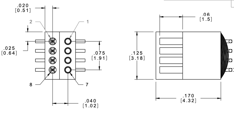
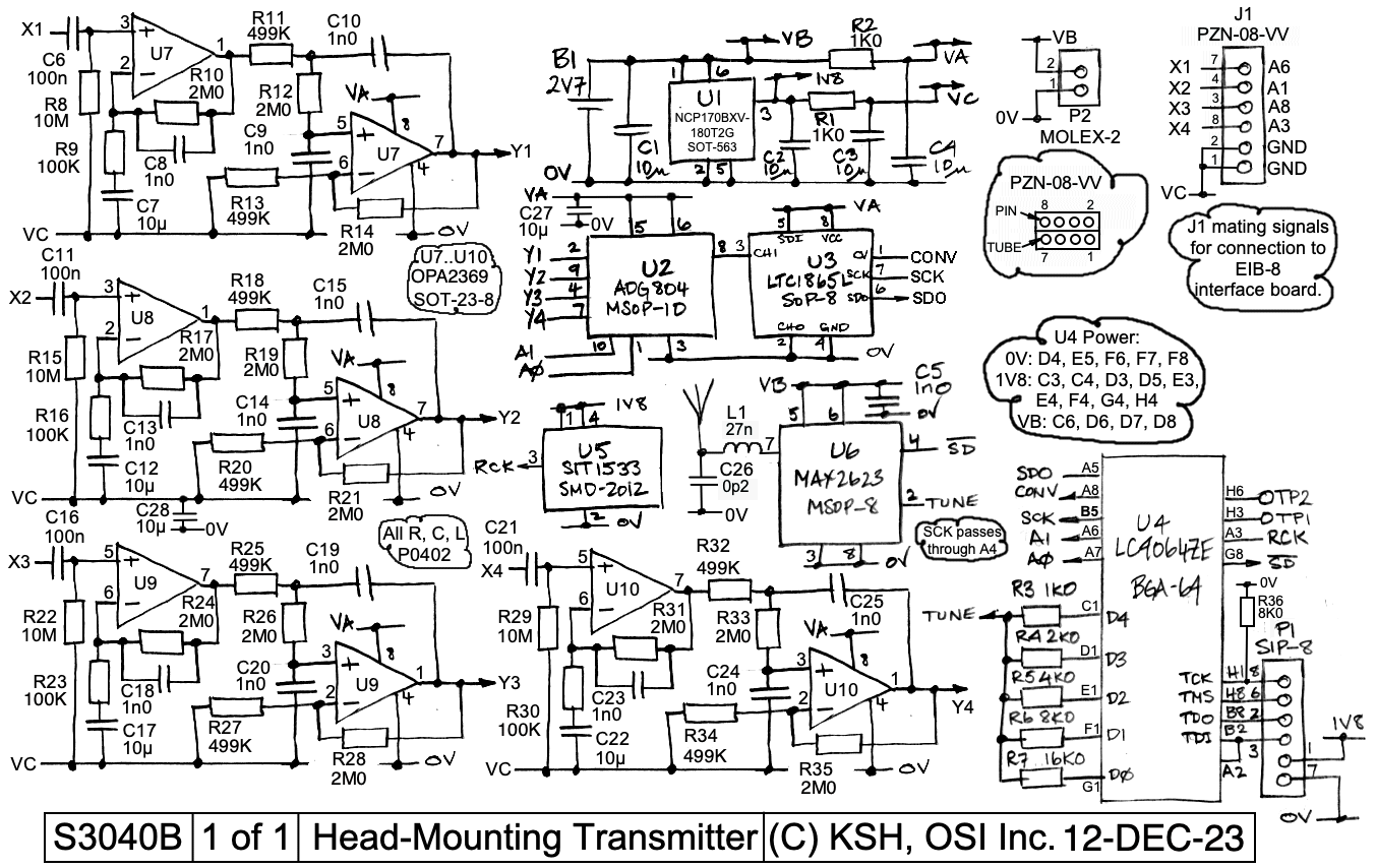
[11-DEC-25] The A3040A provides an eight-way, dual-row, 0.025" pitch, hermaphroditic surface-mount connector, Omnetics PZN-08-VV (A79612), to mate with a connector of exactly the same type on the host animal's head. The connector on the animal's head is part of an Electrode Interface Fixture (EIF). On the HMT circuit diagram, we use the pin numbering given by the manufacturer, see S3040C_1.
| Pin | Function |
|---|---|
| 1 | GND |
| 2 | none |
| 3 | X3 |
| 4 | X2 |
| 5 | none |
| 6 | none |
| 7 | X1 |
| 8 | X4 |
In the HMT circuit diagram, we refer to the reference potential as "VC", the "common voltage". Once we connect this potential to an animal body, we say the HMT is "grounded". Our assumption is the GND wire of the EIF will be used to provide a low-impedance connection to the animal body. On the EIF, the numbers we assign to the pins match the pin numbers on the HMT circuit, but this means they do not match the pin numbers on the manufacturer's data sheet.
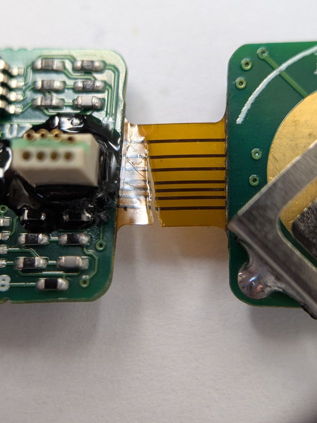
The Electrode Interface Fixture will be equipped with two to five leads. One lead must always be present: the low-impedance ground, which will be connected to Pin 1. On the HMT, we fasten the PZN-08-VV connector to the circuit board with structural epoxy. The pins of the connector are no longer visible, nor can we remove the connector without damaging the circuit board. If we damage the connector tubes or pins, the HMT must be replaced entirely.
[25-OCT-24] The A3040D3 is equipped with four amplifiers with gain ×100 and frequency range 0.3-160 Hz. The A3040D3 samples all four inputs with sample rate 512 SPS. Each sample is a sixteen-bit number 0..65535, where the number zero corresponds to the bottom of the input dynamic range, and 65535 corresponds to the top of the range. The plot below shows their response to a 15-mVpp sinusoidal input with 10-MΩ source resistance as we increase the sinusoidal frequency from 0.25 Hz to 1 kHz. Because the input resistance of the amplifiers is 10 MΩ, we see 7.5 mVpp on each input.
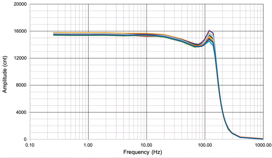
The dynamic range of the inputs is equal to the battery voltage divided by the amplifier gain. For the A3040D3 at 10 Hz, the gain is ×100. The nominal output voltage of the CR-series batteries we use with the HMT is 3.0 V. So the dynamic range is 30 mV. All inputs are referred to a single reference voltage, VC = 1.8 V. The A3040D3 provides a high-pass filter at its inputs. The average value of any of its input is zero. The amplifiers use VC = 1.8 V to represent an input of zero. With battery voltage 3.0 V, an input of zero will be converted to 1.8 V / 3.0 V * 65535 = 39321 cnt (ADC counts). Count zero corresponds to −18 mV at the input, and count 65535 corresponds to +9 mV. The A3040 amplifiers may be configured to provide low-pass cut-off frequencies 40 Hz, 80 Hz, 160 Hz, 320 Hz, and 740 Hz. These cut-off frequencies accompany sample rates 128 SPS, 256 SPS, 512 SPS, 1024 SPS, and 2048 SPS respectively. The low-pass filter is a three-pole Chebyshev filter with some ripple in the pass-band to allow for a sharper cut-off at the top of the pass band. The default high-pass filter is a single-pole RC filter with cut-off at 0.3 Hz. We can remove the high-pass filter to provide response down to 0.0 Hz.

Noise on the A3040D3 inputs in a Faraday enclosure with leads ends in water is 20 cnt rms. Full scale is 30 mV or 65536 counts, so each count is 0.41 μV. We multiply 20 cnt rms by 0.41 μV/cnt to get 8 μV rms. The plot below shows the spectrum of this noise.
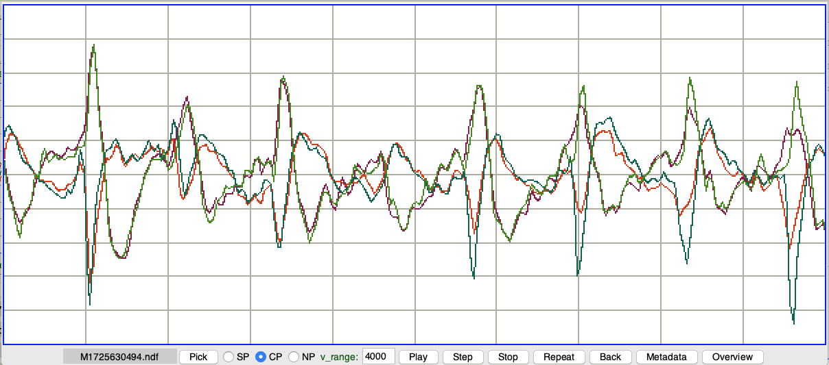
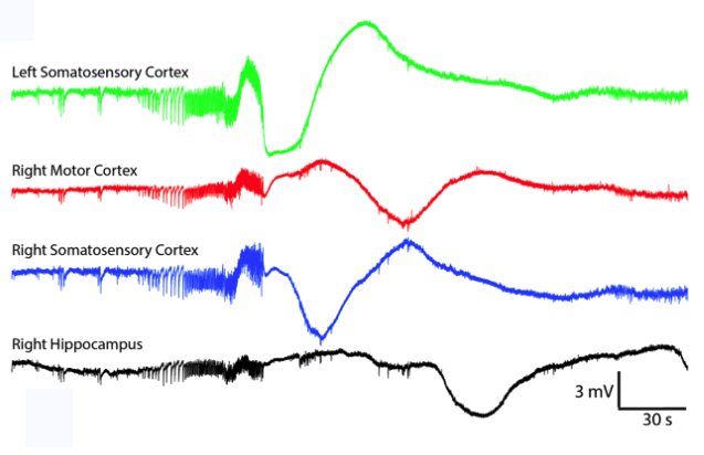
The analog inputs share a single reference potential. We recommend placing this reference potential over the cerabellum and distributing the other four as you see fit. The other four can record electroencephalogram (EEG) or electrocortogram (ECoG) with wire ends, or local field potential (LFP) with depth electrodes. In the example above we have one second of EEG from four electrodes during an ictal event. In order to be sure that the EEG we record on one channel is due only to the potential between that channel's electrode and its reference, we must be assured that the cross-talk between amplifiers is far smaller than the amplitude of the signals we are observing. The plot below shows the amplitude of cross-talk verses frequency when we connect a sinusoid to one input and observe the amplitude recorded by all three channels of a three-channel transmitter.
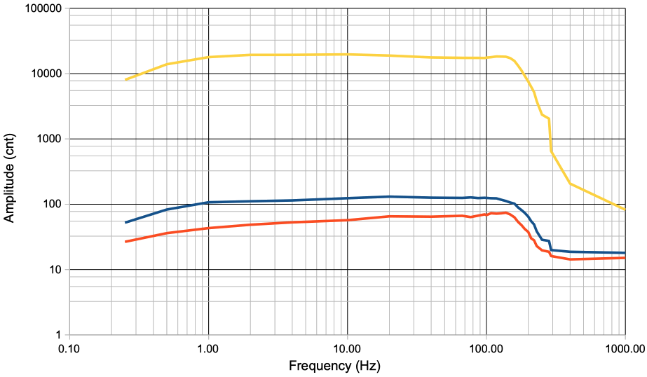
With X3 reporting amplitude 20 mVpp, X1 reports 100 μVpp, X2 reports 50 μVpp. In electrical engineering terms, the crosstalk is −46 dB and −52 dB for X1 and X2.
[30-JUN-25] All A3040s are equipped with non-rechargeable lithium coin cells. When one battery is exhausted, we remove it from the A3040's battery retainer. We can load a new battery whenever we like. The A3040 battery retainer A3040 is designed to hold a CR1225 battery, which is 12.5 mm in diameter and 2.5 mm thick. Without any modification, the retainer will hold a CR927 (2.7 mm thick) or CR1025 (2.5 mm thick). If we bend the retainer's tongue down, the retainer will hold a CR1220 (2.0 mm thick). The CR927, CR1025 reduce the mass of the A3040 by roughly 10% compared to one equipped with a CR1225 battery, but their capacity is 30% less. The CR1220 drops the mass by 5%, but its capacity is 15% less. We assume that our customers will be using the A3040 with CR1225 batteries.
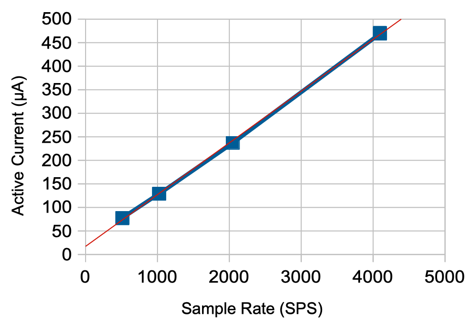
The operating life of an A3040 is how long it can amplify and transmit its input voltages when starting with a fresh battery. We specify the minimum operating life of A3040-family HMTs in the A3040 Version Table. We provide a detailed discussion of the operating life of HMTs and other implantable devices in the Battery Life chapter of our Telemetry Manual. The A3040 has infinite "shelf life", in that we remove its battery when we put it on the shelf, and without its battery it consumes no current.
[11-SEP-24] Installation of the HMT is not in itself a surgery: we are connecting the HMT to an Electrode Interface Fixture (EIF) that has already been installed on the head of the host animal. For general-purpose, step-by-step instructions for fastening an Electrode Interface Fixture (EIF) to an animal's head, see our Surgery for Animal Telemetry page. For a specific protocol provided by one of our customers, see surgical protocol provided by Kate Hills of University of Manchester. This protocol includes a description of how one can attach the HMT in a secure but reversible fasion with the help of Kwik-Cast silicone sealant.
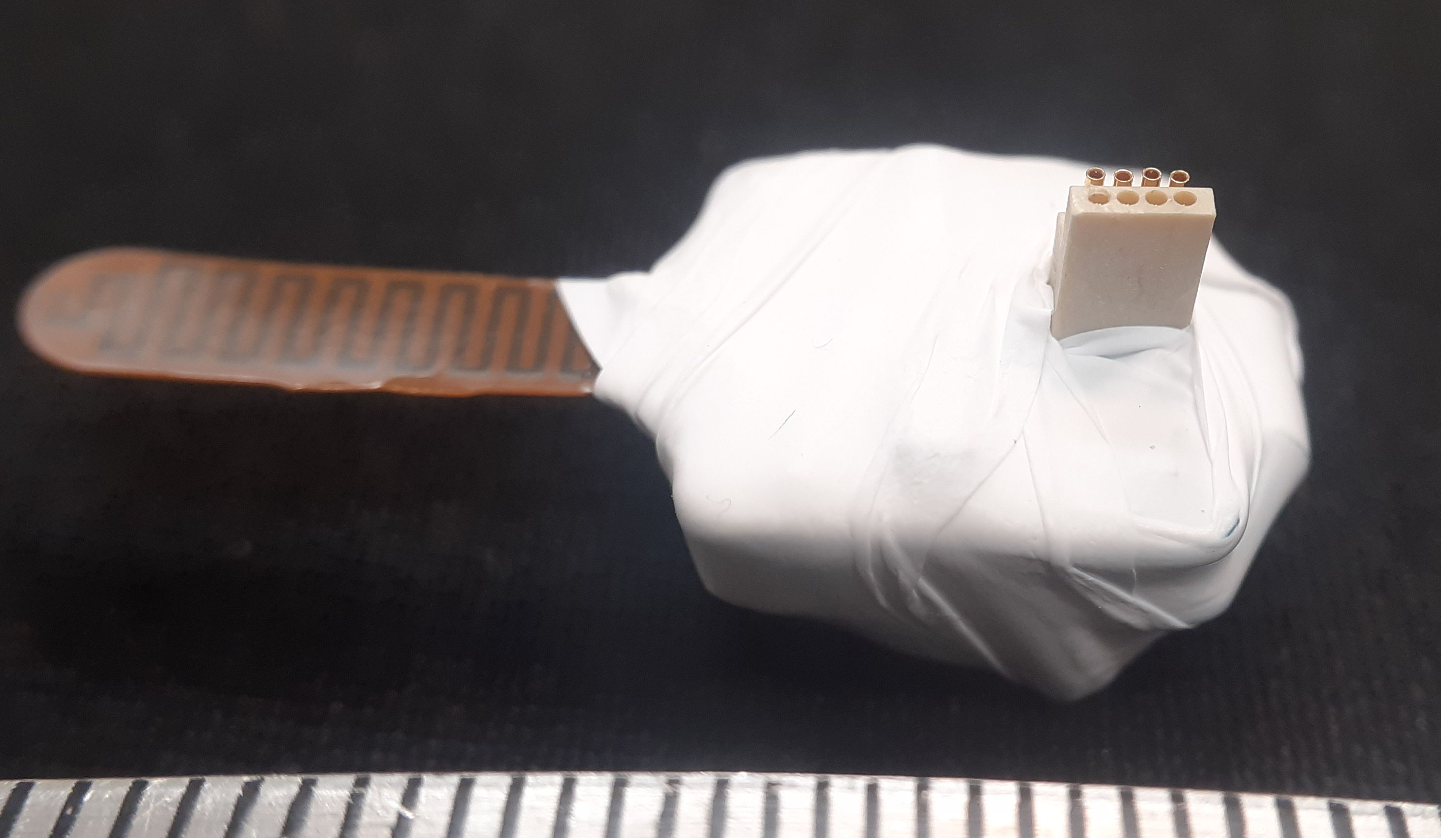
[27-JUN-25] The A3040A has no permanent encapsulation, other than epoxy we apply around its connector to secure the connector in place, and epoxy we apply to the radio-frequency components to protect them from electrostsatic discharge. Before loading the transmitter on the animal, we fold the circuit as shown in our sketch. We wrap the circuit in teflon tape, building up two or three layers, keeping the connector free, and finally adhering the tape to itself. We complete the wrapping with one partial layer of transparent tape, such as Scotch Tape or Sellotape. The teflon wrap stops debris and water getting to the HMT circuit. The transparent tape makes it harder for the mouse to scratch off the teflon tape.
When we replace the battery, we remove the wrapping with our fingers. We do not use scissors because these are likely to touch the circuit inside while it is powered by the battery, and so cause peramanent damage. We remove the battery by pushing it out of its holder with a wooden applicator. We now we have the opportunity to wash the circuit if we like. We rinse in hot water while scrubbing gently with a tooth brush. We blow dry with compressed air. We soak the circuit in ethanol for a few minutes, blow dry, load battery, and wrap with sterile gloves.
Any water-proof tape that adheres well to itself is a likely candidate for wrapping the HMT during use. Self-fusing silicone tape is rugged and water-proof, but adds 0.5 g to the transmitter mass, see here. Plumber's teflon tape is thinner, and adds only 0.2 g to the mass. The British clingfilm adds only 0.2 g, see here. Parafilm adds 0.2 g see here. Gardener's tape adds only 0.2 g as well, see here. Our customers have obtained best results with a two-tape wrap. Begin with teflon plumber's tape, then hold the plumber's tape in place with a layer of transparent paper tape, also called "cellotape" and "scotch tape".
[27-JUN-25] To mount a Head-Mounting Transmitter (HMT) on its Electrode Interface Fixture (EIF), hold the animal's head in one hand. Looking from the side, push the HMT onto the EIF. Once the connectors are mated, with no gap between their housings, apply Kwik-Cast silicone sealant around the joint between the connectors. The sealant will make sure the mouse is unable to wiggle the HMT off its connector.
To unmount the HMT, hold the animal's head in one hand between thumb and forefinger. Remove the Kwik-Cast with tweezers from all around the connector. Hold the HMT in your other hand and rock it slightly back and forth along perpendicular to its length. The two connectors will slowly work themselves apart until they separate. Do not attempt to pull the HMT off directly, because doing so generates so much force that the EIF may tear off the animal's skull. During this process, some of our customers prefer to sedate the mouse so as to facilitate the removal and avoid frightening the animal. Some customers prefer to avoid the use of sedative because the sedative might interfere with their study.
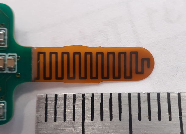
[08-FEB-23] The antenna on the A3040 is a flexible circuit with a rounded end. Counting the neck at its base, the antenna is 14 mm long. It is 4 mm wide. It carries a zig-zag conductor of total length 70 mm, which is slightly less than one quarter of the wavelength of our telemetry transmissions. We transmit in 902-928 MHz, for which the wavelength is around 330 mm.
The A3040AV1 provides footprints for a series-parallel matching network between the circuit's radio-frequency (RF) oscillator and the antenna. The AV1 does not attempt to match the antenna to the oscillator: the two are coupled with a single 1 nF capacitor. But the AV2 loads 27 nH for L1 and 0.2 pF for C26 to increase power output by a factor of ten.
[22-JAN-26] The HMT is designed to be used repeatedly. We replace the battery and wrap it again. Unlike our implantable transmitters, the HMT is not encapsulated in epoxy. When in use, it is not immersed in body fluid at 37°C. It is not vulnerable to corrosion. But it is vulnerable to scratching and abrasion. If an HMT becomes detached during an experiment, it is likely to be destroyed by its host. Furthermore, while cutting off our wrapping, we might cut through one of the flex circuits. By pushing on the circuit board with a metal tool, we might crack one of the HMT's ceramic capacitors. We offer no warranty against such unfortunate events. But we do offer a two-year warranty against manufacturing defects, such as bad solder joints.
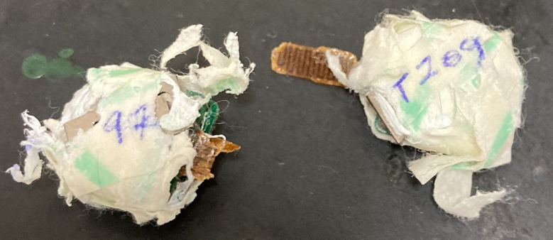
An experienced user of HMTs can expect something like sixty days of operation from each device. In a survey of twenty-one HMTs deployed on single-housed animals over three years at the Institute of Neurology in London, thirteen failed and six remain functional. Nine failed because the flex antenna was chewed through or pulled off. Three failed because the connector was chewed. One failed because the battery tab was ripped from the circuit board, pulling off its mounting pad in the process. Among those that failed, the number of times the HMT was mounted for use before failure varied from once to nineteen times, with an average of five. The number of days for which the HMT provided telemetry signals varied from 8 to 180 days, with an average of 60 days. Among those that have not yet failed, the number of uses varies from two to fifteen with an average of six. The number of days running varies from 25 to 215 days with an average of 82 days. Given these observations, we recommend that HMT users plan their experiments with the assumption that any given HMT has a 2% chance of being pulled off and damaged on any given day. If we have ten HMTs deployed, we can expect one of them to fail every week. The operating cost of HMTs is approximately 2% of their purchase price per day, not counting labor and overhead.
As the foregoing observations and conclusion make plain: the vulnerability of the HMT to physical damage during threatens to undermine any experiment we plan to perform with the devices. To streamline your experiment and speed up HMT replacement, we recommend purchasing HMTs in matching pairs. So far as the data acquisition system is concerned, the two HMTs in a pair are identical because they use the same channel numbers for their telemetry signals. With two identical HMTs for each animal, you can prepare the replacement HMT with a fresh battery, pick up the animal, remove the expiring HMT, load the fresh HMT, apply more silicone fastener, and put the animal back in the cage in less than a minute. You do not have to take the expiring HMT, unwrap it, clean it, replace the battery, check it's running, wrap it, and go back to the animal room. You have ample time to clearn, dry, and prepare the new HMT before the replacement takes place. Your telemetry recordings are simplified: each animal is associated with only one set of channel numbers. Once you have your pairs of HMTs established, you can order replacements from us to maintain your collection.
[30-JUL-25] For design files and development logbook, see the A3040 design and development page at D3040.