[03-MAR-25] The Subcutaneous Transmitter (A3049) is an implantable telemetry sensor for mice and rats that provides amplification and filtering for up to two, independent biopotentials. When equipped with a small coin cell, it is fits comfortably in a mouse. When equipped with a large coin cell, it fits comfortably in a rat. The A3049 operates with our Subcutaneous Transmitter system. We turn the A3049 on and off with a magnet.

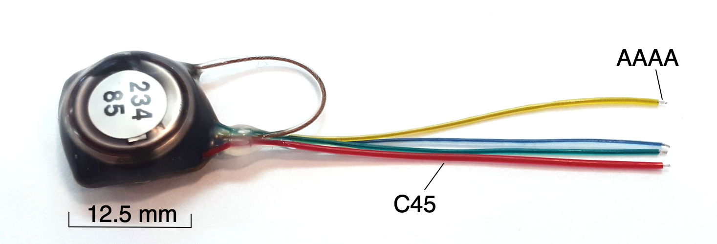
The A3049 amplifier can be configured to provide gain of anywhere from ×10 to ×100. The low-pass filter can be configured for a corner frequency of 20 Hz, 40 Hz, 80 Hz, 160 Hz, 320 Hz, or 640 Hz. The high-pass filter on the amplifier input can be configured to provide a corner frequency of 0.2 Hz or 2 Hz, but can also be removed entirely, so as to provide gain all the way down to 0.0 Hz (DC). The logic may be programmed to sample at 64, 128, 256, 512, 1024, or 2048 SPS, so as to suite the corner frequency of the low-pass filter. The standard leads we use with the A3049 are our 0.7-mm diameter colored, silicone-insulated, stainless steel helical leads, along wiht a clear, silicone-insulated, stranded-steel loop antenna. The length of the leads, the battery loaded next to the circuit, the operating life, the termination of the leads, the sample rate, the gain of the amplifier, and the bandwidth of the amplifier all vary from one version to the next, depending upon the configuration.
The A3049 may be configured as a single or dual-input sensor. As a single-input sensor it will transmit one signal on one telemetry channel. As a two-input sensor it will transmit two signals on two telemetry channels. The first channel number will always be an odd-numbered channel. The leads loaded on the transmitter depend upon its "input configuration", as shown below.
| Type | Input Configuration | X+ | X− | Y+ | Y− | Applications |
|---|---|---|---|---|---|---|
| I | Single-Input, X Amplifier | Red | Blue | Omitted | Omitted | EEG, EMG, ECG, or EGG |
| II | Single-Input, Y Amplifier | Omitted | Omitted | Yellow | Green | none |
| III | Dual-Input, Common Reference | Red | Blue (Shared) | Yellow | Blue (Shared) | EEG+EEG |
| IV | Dual-Input, Separate References | Red | Blue | Yellow | Green | EEG+EMG, EMG+EGG, EEG+ECG |
Each transmitter has a label providing two numbers. The first is a batch number, B, the second is a telemetry channel number, N. A single-channel transmitter uses channel N only. A dual-channel transmitter uses channel N for the X input and N+1 for the Y input. In a dual-channel transmitter, N is always odd.
| Property | Specification |
|---|---|
| Volume | 1.2±0.1 ml |
| Mass | 2.2±0.1 g |
| Operating Life | 14 days |
| Battery Capacity | 2000 μA-days |
| Shelf Life | 6 months |
| On-Off Control | magnet |
| Input Configuration | III, Dual-Input, Common Reference |
| Lead Dimensions | diameter 0.7±0.1 mm, length 45±2 mm |
| Lead Terminations | steel coil, diameter 0.45 mm, length 1.0 mm |
| Input Impedance | 10 MΩ |
| Sample Rate | 512 SPS each channel |
| Bandwidth | X: 0.24-160 Hz, Y: 0.16-160 Hz |
| Noise | <6 μV rms |
| Distortion | <0.1% |
| Dynamic Range | 30 mV (−18 mV to +12 mV) |
| Resolution | 16-bit |
| Absolute Maximum Input Voltage | ±3 V |
All versions of the A3049 are covered by a one-year warranty against corrosion and manufacturing defect.
[26-FEB-25] There are many possible configurations of the SCT. Each configuration that someone has ordered, or asked us to quote on, graduates from being a mere "configuration" to a "version". We describe and list the available SCT versions in the section below. At the time of writing, the minimum order quantity for any particular version is one piece, but the price drops significantly if you order six or more of the same exact version. To get a quotation or to discuss which transmitters will best meet your study's needs, please email us at info@opensouresintruments.com.
[13-APR-25] The Subcutaneous Transmitter (A3049) can be equipped with a dozen different batteries, any lead length up to 280 mm, several lead diameters, one or two recording channels, a dozen varieties of lead terminations, several types of antenna, and a range of bandwidths, gains, and sample rates. You specify which transmitter you want with a full SCT part number. The part number begins with A2049 and is followed by the primary version letter that tells us the battery we load on the circuit, and the input configuration. Following the letter we have one or two more numbers and letters that specify the sample rate of the inputs. We use the numbers 1-5 to indicate 128, 256, 512, 1014, and 2048 SPS respectively. We use the letter "Z" to indicate that the low end of the frequency response reaches all the way down to 0.0 Hz. After a dash we have a number and letter to specify the length and type of the leads. After a second dash we have letters specifying the electrodes, and after a final dash we have a letter specifying the antenna.
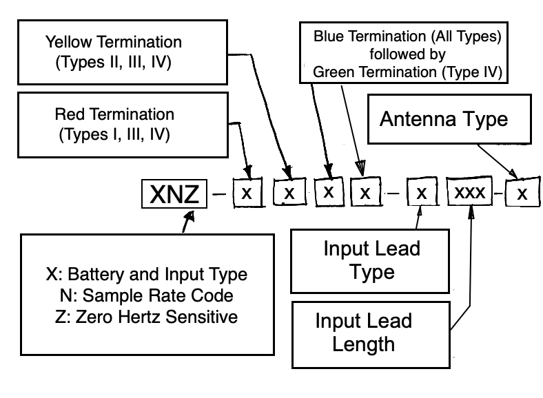
See our Electrode Catalog for a list of terminations and of depth electrodes to which our terminations can be attached. See our Lead Table for a description of our several types of insulated, helical steel leads. See our Antenna Table for a description of the various types of antenna we can deploy on our implants. The table below lists the A3028 primary version codes. Battery capacities are usually expressed in units of mA-hr. We convert to μA-dy so it is easier to divide the capacity by the active current and obtain the operating life in days. We give frequency response in Hertz, sample rate in samples per second, and dynamic range of each input in millivolts. The operating life is the minimum time for which a newly-made transmitter will operate continuously. The shelf life is the time the transmitter can remain turned off in storage and still retain 90% of its operating life. Input resistance is either 10 MΩ or 20 MΩ, see Amplifiers.
| Version | Inputs | X | Y | Battery Capacity (μA-dy) |
Volume (ml) |
Mass (g) |
Operating Life (dy) |
Shelf Life (mo) |
|---|---|---|---|---|---|---|---|---|
| A3049W1 | III | 0.24-40 Hz, 128 SPS, 30 mV | 0.16-40 Hz, 128 SPS, 30 mV | 1650 (CR1220) | 1.1 | 2.0 | 34 | 6 |
| A3049W1Z | III | 0.0-40 Hz, 128 SPS, 120 mV | 0.0-40 Hz, 128 SPS, 120 mV | 1650 (CR1220) | 1.1 | 2.0 | 34 | 6 |
| A3049A2 | III | 0.24-80 Hz, 256 SPS, 30 mV | 0.16-80 Hz, 256 SPS, 30 mV | 2000 (CR1225) | 1.2 | 2.2 | 24 | 7 |
| A3049A2Z | III | 0.0-80 Hz, 256 SPS, 120 mV | 0.0-80 Hz, 256 SPS, 120 mV | 2000 (CR1225) | 1.2 | 2.2 | 24 | 7 |
| A3049A3 | III | 0.24-160 Hz, 512 SPS, 30 mV | 0.16-160 Hz, 512 SPS, 30 mV | 2000 (CR1225) | 1.2 | 2.2 | 14 | 7 |
| A3049A3Z | III | 0.0-160 Hz, 512 SPS, 120 mV | 0.0-160 Hz, 512 SPS, 120 mV | 2000 (CR1225) | 1.2 | 2.2 | 14 | 7 |
| A3049A4 | III | 0.24-320 Hz, 1024 SPS, 30 mV | 0.16-320 Hz, 1024 SPS, 30 mV | 2000 (CR1225) | 1.2 | 2.2 | 7 | 7 |
| A3049B2 | I | 0.24-80 Hz, 256 SPS, 30 mV | Disabled | 2000 (CR1225) | 1.2 | 2.2 | 39 | 7 |
| A3049B3 | I | 0.24-160 Hz, 512 SPS, 30 mV | Disabled | 2000 (CR1225) | 1.2 | 2.2 | 25 | 7 |
| A3049B4 | I | 0.24-320 Hz, 1024 SPS, 30 mV | Disabled | 2000 (CR1225) | 1.2 | 2.2 | 14 | 7 |
| A3049J2 | IV | 0.24-80 Hz, 256 SPS, 30 mV | 0.16-80 Hz, 256 SPS, 30 mV | 2000 (CR1225) | 1.2 | 2.2 | 25 | 7 |
| A3049J3 | IV | 0.24-160 Hz, 512 SPS, 30 mV | 0.16-160 Hz, 512 SPS, 30 mV | 2000 (CR1225) | 1.2 | 2.2 | 14 | 7 |
| A3049J3Z | IV | 0.0-160 Hz, 512 SPS, 120 mV | 0.0-160 Hz, 512 SPS, 120 mV | 2000 (CR1225) | 1.2 | 2.2 | 14 | 7 |
| A3049J4 | IV | 0.24-320 Hz, 1024 SPS, 30 mV | 0.16-320 Hz, 1024 SPS, 30 mV | 2000 (CR1225) | 1.2 | 2.2 | 8 | 7 |
| A3049J4Z | IV | 0.0-320 Hz, 1024 SPS, 120 mV | 0.0-320 Hz, 1024 SPS, 120 mV | 2000 (CR1225) | 1.2 | 2.2 | 8 | 7 |
| A3049F2 | I | 0.24-80 Hz, 256 SPS, 30 mV | Disabled | 3300 (CR1620) | 1.4 | 2.9 | 65 | 10 |
| A3049H2 | III | 0.24-80 Hz, 256 SPS, 30 mV | 0.16-80 Hz, 256 SPS, 30 mV | 3300 (CR1620) | 1.4 | 2.9 | 40 | 10 |
| A3049H2Z | III | 0.0-80 Hz, 256 SPS, 120 mV | 0.0-80 Hz, 256 SPS, 120 mV | 3300 (CR1620) | 1.4 | 2.9 | 40 | 10 |
| A3049H3Z | III | 0.0-160 Hz, 512 SPS, 120 mV | 0.0-160 Hz, 512 SPS, 120 mV | 3300 (CR1620) | 1.4 | 2.9 | 23 | 10 |
| A3049K1 | IV | 0.24-40 Hz, 128 SPS, 30 mV | 0.16-80 Hz, 64 SPS, 30 mV | 3300 (CR1620) | 1.4 | 2.9 | 75 | 10 |
| A3049D2 | III | 0.24-80 Hz, 256 SPS, 30 mV | 0.16-80 Hz, 256 SPS, 30 mV | 11000 (CR2330) | 2.6 | 5.8 | 139 | 36 |
| A3049D3 | III | 0.24-160 Hz, 512 SPS, 30 mV | 0.16-160 Hz, 512 SPS, 30 mV | 11000 (CR2330) | 2.6 | 5.8 | 81 | 36 |
| A3049D4 | III | 0.24-320 Hz, 1024 SPS, 30 mV | 0.16-320 Hz, 1024 SPS, 30 mV | 11000 (CR2330) | 2.6 | 5.8 | 43 | 36 |
| A3049E3 | I | 0.24-160 Hz, 512 SPS, 30 mV | Disabled | 11000 (CR2330) | 2.6 | 5.8 | 139 | 36 |
| A3049Q3 | III | 0.24-160 Hz, 512 SPS, 30 mV | 0.16-160 Hz, 512 SPS, 30 mV | 25000 (CR2450) | 4.0 | 8.7 | 184 | 82 |
| A3049Q3Z | III | 0.0-160 Hz, 512 SPS, 120 mV | 0.0-160 Hz, 512 SPS, 120 mV | 25000 (CR2450) | 4.0 | 8.7 | 184 | 82 |
| A3049Q4 | III | 0.24-320 Hz, 1024 SPS, 30 mV | 0.16-320 Hz, 1024 SPS, 30 mV | 25000 (CR2450) | 4.0 | 8.7 | 100 | 82 |
| A3049T5 | I | 0.24-640 Hz, 2048 SPS, 30 mV | Disabled | 25000 (CR2450) | 4.0 | 8.7 | 100 | 82 |
| A3049L4 | III | 0.24-320 Hz, 1024 SPS, 30 mV | 0.16-320 Hz, 1024 SPS, 30 mV | 42000 (CR2477) | 6.0 | 14.0 | 168 | 140 |
For analog input we specify the bandwidth, sample rate, input dynamic range, and channel number offset. In terms of ADC counts, the dynamic range is always 0-65535, as produced by a sixteen-bit ADC. The zero-value of an input is the sample we obtain when we short the two inputs together. The zero-value depends upon the battery voltage, VB, according to zero-value = 1.8 V × 65535 ÷ VB. The dynamic range is the battery voltage divided by the gain of the amplifier. When we specify dynamic range, we assume VB = 3.0 V, which is true for the first half of the life of a CR-series lithium battery at 37°C. When the amplifier gain is 100, the dynamic range is 30 mV distributed on either side of zero as −18 mV to +12 mV.
See below for details of current consumption and how to calculate battery life of new versions of the A3049. By default, we set the top of the frequency range at one third the sample rate. The A3049's low-pass filters provide 20 dB of attenuation at one half the sample rate. Frequencies above one half the sample rate will be distorted by sampling, and so compromise the fidelity of the recording. Because the EEG signal contains less and less power as frequency increases, this attenuation is sufficient to ensure that distortion is insignificant.
[07-FEB-25] The A3049 provides up to four signal inputs: X+, X−, Y+, and Y−. Each of these inputs has a reserved color for its leads: red, blue, yellow, and green respectively. These four leads are present or absent in accordance with each transmitter's input configuration. Whenever the X+ (red) lead is present, it uses the X− (blue) lead as its reference potential. When the Y+ (yellow) lead is present without the Y− (green) lead, the Y+ lead uses the X− lead as its reference potential. When the Y− lead is present, the Y+ uses the Y− lead as its reference potential. When equipped with three leads, the A3049 is a two-channel sensor with a shared reference potential. When equipped with four leads, it is a two-channel sensor with separate reference potentials.
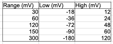
We specify for each analog input its absolute dynamic range, which is the difference between the high and low potentials at which the amplifier will saturate. The table above gives these high and low potentials for each standard A3049 input dynamic range.

The impedance of X input, as seen at the tips of its electrode leads, is 10 MΩ. When the Y input uses X− as its reference, the Y input impedance is 10 MΩ. When the Y input uses Y− as its reference, the Y input impedance is 20 MΩ. Most transmitters provide a high-pass filter by placing a capacitor in series with the input. The corner frequency of this high-pass filter is 0.2 Hz. When the input impedance is 10 MΩ, the high-pass filter presents a 100-nF capacitor in series with the input, and when the input impedance is 20 MΩ, the series capacitance is 50 nF. When we modify the transmitter to remove the high-pass filter, these capacitors will not be present at the input.
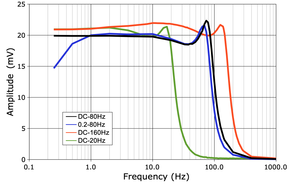
The X signal is supposed to be a measure only of difference between X+ and X−. The average voltage of X+ and X− is the common mode voltage on X, and the difference between X+ and X− is the differential mode voltage. Suppose we apply the same sinusoidal voltage to both X+ and X−. The common mode voltage is the sinusoidal voltage and the differential mode voltage is zero. Under these circumstances, we would like X to be zero, but instead we will see a trace of the common-mode voltage appearing in the X signal. The ratio of the common-mode voltage amplitude and the X signal amplitude is the common mode rejection ratio, or CMRR. The plot below shows how the CMRR of X and Y vary with frequency.

The X-input provides CMRR of 40 dB for frequencies for frequencies below 160 Hz. The signal we see on X will be 1% the amplitude of the common-mode signal we apply to X. The CMRR of the Y-input is >40 dB for frequencies below 10 Hz, but drops for higher frequencies.
The distortion of a signal by our telemetry system is the extent to which it changes the shape of a signal. We apply a 10 mVpp sinusoid to the X and Y inputs of an A3049AV3. The AV3 is equipped with two 160-Hz amplifiers. Input dynamic range is 30 mV. We increase the frequency from 1/8 Hz to 200 Hz. For each frequency, we obtain the spectrum of the signal and measure the power outside the sinusoidal frequency as a fraction of the sinusoidal power using this script. We express the result in parts per million.

The distortion of the X is dominated by random electronic noise. There are no significant peaks in the spectrum outside the fundamenta.

We note that the distortion generated by the A3049 is hundreds of time less powerful than that of its predecessor, the A3028. The A3049 samples the signal uniformly, thus eliminating the scatter noise present in the A3028 signal.
[22-JAN-25] If the offsets in our two amplifiers are both zero, and the on-board 1.8-V voltage regulator produces exactly 1.80 V, then we can deduce the transmitter's battery voltage using the following formula.
Where VB is the battery voltage and AVE is the average value of either X or Y in ADC counts. In practice, this formula is accurate to ±0.1 V provided the battery voltage is ≥2.4 V. The plot below shows how the average X and Y vary as we decrease battery voltage from 3.4 V down to the minimum operating voltage of the transmitter, which is 1.8 V.
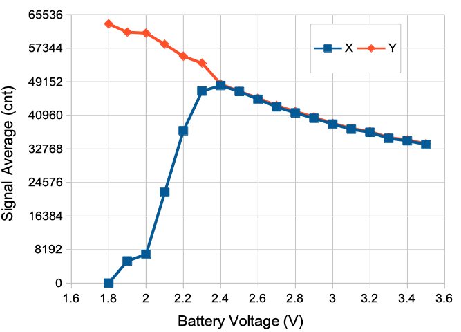
As the battery voltage drops below 2.4 V, the X signal drops towards zero, while the Y signal continues to rise.
[19-APR-23] When we want to mark in our SCT recordings the time at which some event took place, such as the start of a video recording, the moment that a light was flashed, or when an noise commenced, we can use an auxiliary SCT to record a synchronizing signal along with the signals received from implanted SCTs. See the Synchronization section of the A3028 manual for details.
[19-APR-23] See Body Capacitance in the A3019 manual.
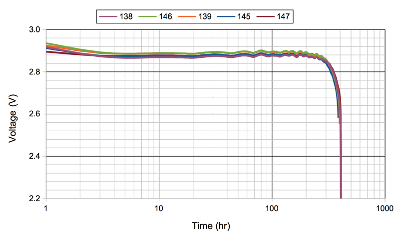
[23-OCT-24] We equip all our subcutaneous transmitters with CR-series lithium primary cells. The voltage produced by these batteries begins at around 3.2 V, drops rapidly to 3.0 V, remains around 2.9 V for most of the battery's life, and drops rapidly towards the end of life.
The inactive current consumption of the A3049, which is its current consumption when it is turned off, is roughly 0.8 μA at room temperature. When we calculate shelf life, however, we use 1.0 μA for the inactive current consumption, so as to arrive at a conservative estimate of the time it will take for the A3049 to use 10% of its battery while sitting on the shelf. The CR1225 battery has capacity 50 mAhr ≈ 2000 μAdy, so its shelf life is 200 dy = 7 mo.
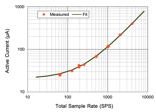
To obtain the operating life of an A3049 transmitter, we divide the battery capacity in μA-days by the maximum current consumption in μA, and then subtract one day. The subtraction of one day is necessary to account for the twenty-four hours of testing we perform on each transmitter during quality control. To obtain the maximum current consumption of an A3049 transmitter, we use the following relation.
In the above relation, we have 22 μA base current consumption, which powers the logic chip (15 μA), amplifiers (4 μA), and miscellaneous circuits (2 μA). Additional current consumption by digitization and transmission is 0.11 μA per sample per second, or we could say that each sample requires 0.11 μC of charge drawn from the battery. The above formula predicts 50 μA for 256 SPS. The average current consumption of the A3049 circuits is roughly 10% lower than the maximum.
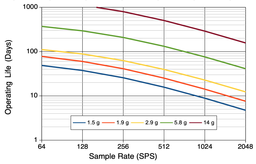
In the table below, we use our formula for maximum current consumption and combine it with the nominal capacity of the batteries we might use with the A3049. The CR1620 is the smallest battery we believe we can load onto the 20-mm diameter circuit. The CR2477 is the largest battery we know for sure that a large adult rat can tolerate.
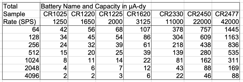
In each of the above entries, we have divided the nominal capacity of the battery by the maximum current consumption and subtracted one from the result to obtain our guaranteed operating life.
[29-NOV-23] All versions of the A3049 are encapsulated in black epoxy and coated with silicone. The silicone is "unrestricted medical grade" MED-6607, meaning it is approved for implants of unlimited duration in any animal, humans included. The A3049's leads and antenna are encapsulated with dyed silicone, then coated with the same unrestricted medical grade silicone. The only materials the transmitter and its leads present to the subject animal's body are either unrestricted medical grade silicone or stainless steel. When we solder screws or pins to the ends of the leads, there is also solder. Solder reacts slowly with saline, so solder joints must be protected from body fluids by an insulating layer of cement during implantation.
[24-MAR-25] The following table lists versions of the assembled A3049 electronic circuit, out of which we make the A3049-series transmitters.
| Version | Description |
|---|---|
| A3049AV1 | X=0.24-160Hz, Y=0.16-80Hz, U4=U5=MAX4474, R21=10M |
| A3049AV2 | X=0.24-160Hz, Y=0.16-80Hz, U4=U5=MAX4474, R21=10M |
| A3049AV3 | X=0.24-160Hz, Y=0.16-160Hz, U4=MAX4474, U5=OPA2369, antenna protection, R21=100K |
| A3049AV4 | X=0.24-80Hz, Y=0.16-80Hz |
| A3049BV1 | X=Y=0.16-160Hz, U4=U5=OPA2369, U10=ASZKDV, some new designations. |
Details of the design are available in the following library of design files. Note that all our designs are protected by the GNU General Public Lisence. We begin with the A3049AV1 through A3049AV4 assemblies, which were in production 2023-2024.
S3049AV1_1.gif: Schematic of A3049AV1 assembly.Starting in March 2025, we move to the A3049BV1 assembly, which uses a ceramic crystal oscillator instead of the former epoxy-encapsulated MEMS oscillator, in an effort to extend corrosion resistance. The footprint for the oscillator will accommodate several different parts available in the X2012 package. The new assemblies use the OPA369 op-amp with its lower offset voltage to improve the accuracy of battery voltage measurements, renames some parts, adjusts capacitor values to reduce start-up current. Single-channel transmitters requiring response up to 640 Hz will have to be made with the MAX4474 or OPA2349 loaded for U4.
S3049BV1_1.gif: Schematic for A3049BV1, ceramic oscillator, re-named components.[02-OCT-24] Here we list the electronic circuits we can use to assemble the various types of A3049 transmitter, and the modifications required by that circuit prior to assembly. Roman numerals give the input configuration.
| Configuration | Inputs | Assembly | C2 C3 |
C7 | R8 | C8 | C9 C10 C11 |
C12 | R15 | C13 C14 C15 |
C16 | R21 |
|---|---|---|---|---|---|---|---|---|---|---|---|---|
| A3, H3, D3, Q3 | III | AV3 | 1.0 μF | |||||||||
| A4, H4, D4, Q4 | III | AV3/AV4 | 1.0 μF | 510 pF | 510 pF | |||||||
| B3, F3, E3 | I | AV3 | 1.0 μF | |||||||||
| B3, F3, E3 | I | AV4 | 1.0 μF | 1.0 nF | ||||||||
| A2, H2, D2, Q2 | III | AV4 | 1.0 μF | |||||||||
| B2, F2, E2 | I | AV4 | 1.0 μF | |||||||||
| K1 | IV | AV4 | 1.0 μF | 3.9 nF | 1.0 μF | 1.0 MΩ | ||||||
| J2 | IV | AV4 | 1.0 μF | 1.0 μF | 1.0 MΩ | |||||||
| J3 | IV | AV3 | 1.0 μF | 1.0 μF | 1.0 MΩ | |||||||
| J4 | IV | AV3/AV4 | 1.0 μF | 510 pF | 510 pF | 1.0 μF | 1.0 MΩ | |||||
| J3Z | IV | AV3 | 1.0 μF | 1.0 kΩ | 499 kΩ | 1.0 kΩ | 1.0 kΩ | 499 kΩ | 1.0 kΩ | 10 MΩ | ||
| J4Z | IV | AV3/AV4 | 1.0 μF | 1.0 kΩ | 499 kΩ | 1.0 kΩ | 510 pF | 1.0 kΩ | 499 kΩ | 510 pF | 1.0 kΩ | 10 MΩ |
| A3Z, H3Z, D3Z, Q3Z | III | AV3 | 1.0 μF | 1.0 kΩ | 499 kΩ | 1.0 kΩ | 1.0 kΩ | 499 kΩ |
The most complicated modifications are for our 0.0-Hz transmitters, which are those with suffix "Z". In these we must remove the high-pass filter on each amplifier and reduce the ampifier gain to provide greater dynamic range. We replace two or three capacitors with 1-kΩ resistors. We replace two 100 kΩ with 499 kΩ to provide a gain of ×25 instead of ×100, and a dynamic range of 120 mV instead of 30 mV.
[23-OCT-24] For details of the development and production of the A3049, see its Developement page.