Subcutaneous Transmitter (A3028)
© 2013-2025, Kevan Hashemi,
Open Source Instruments Inc.
Copyright: The software, drawings, schematics, and manuals presented here are distributed for free under the GNU General Public License. If you modify this work, or include it in your own work, you must distribute the resulting work for free under the same license.
Warranty: Our software, firmware, drawings, schematics, and manuals are free, and carry absolutely no warranty. Our hardware carries a warranty of five years against manufacturing defect, with the exception of implantable devices, which carry a warranty of one year.
Contents
Warnings
Description
Versions
Electrodes
Leads
Antenna
Design
Modifications
Analog Inputs
Synchronization
Input Noise
Power Measurement
Body Capacitance
Battery Life
Encapsulation
Development
Description
Retirement Notice: The A3028 is no longer in production. It has been replaced by the One-Channel SCT (A3048), the Two-Channel Transmitter (A3049) and the Four-Channel Transmitter (A3049).
[01-NOV-22] The Subcutaneous Transmitter (A3028) is an implantable telemetry sensor for rats and mice that provides high-fidelity amplification and recording of one or two biopotential inputs. The A3028 operate within our Subcutaneous Transmitter system.

Figure: Subcutaneous Transmitter A3028A3-CCC-B45-B. Body 13 mm × 13 mm × 8 mm, volume 1.2 ml, mass 2.2 g. The leads are 45 mm long and 0.7±0.1 mm in diameter. First recording channel is Red − Blue, second is Yellow − Blue. Lead terminations are M0.5 screws soldered to the stainless steel coil of the lead.
The A3028A2 displaces 1.2 ml, weighs 2.2 g and provides two EEG channels with bandwidth 0.3-80 Hz. It runs for a minimum of 24 days. The A3028E3 displaces 2.6 ml, weighs 5.8 g, and provides one 0.3-160 Hz EEG channel. It runs for 132 days. Both the A3028A3 and A3028E3 are fully-implantable beneath the skin of an animal.


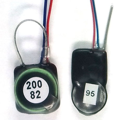
Figure: Subcutaneous Transmitter A3028B-AA-B45-B and A3038P1-AA-C37-C Seen From Top (Left) and Side (Right). The A3028B is on the left in each picture. It has volume 1.3 ml and is equipped with 0.7-mm diameter leads and a 30-mm loop antenna. The A3028P is on the right in each picture. It has volume 0.65 ml and is equipped with 0.5-mm leads and a 13-mm helical antenna.
All current versions of the A3028 are equipped with non-rechargeable lithium primary cells. We warranty all our implantable devices against corrosion and manufacturing defect for one year after delivery. We do not warranty the devices against damage during explantation. You can follow our soldering instructions to repair damaged leads. We no longer manufacture rechargeable versions of the A3028. For transmitters with replaceable batteries, see the Head-Mounting Transmitter (A3040).

Figure: Subcutaneous Transmitter A3028Q-PPP-B150-A. Volume 4.5 ml, diameter 24 mm, depth 11 mm, mass 8.8 g. The three leads are 130 mm long and 0.7 mm in diameter with 3-mm bare wire terminations (B-Leads with P-Coils). The antenna is a 50-mm loop of stranded steel (A-Antenna).
We turn the A3028 on and off with a magnet. We recommend a cow magnet. The A3028A comes with three helical stainless-steel leads coated with silicone. The three leads provide us with two biopotential inputs, red and yellow, that share a common ground, blue. The sensor measures the voltage difference Red − Blue and Yellow − Blue. The lead terminations can be screws, pins, or bare wire, as we discuss in Electrodes and The Source of EEG.
| Property | Value |
|---|
| Volume of Transmitter Body | 1.2 ml |
| Mass of Transmitter Body | 2.2 g |
| Lead Dimensions | diameter 0.7±0.1 mm, length up to 130 mm |
| Maximum Dimensions | 14 mm × 14 mm × 8 mm |
| Minimum Operating Life | 14 days |
| Shelf Life | 5.5 years |
| Number of Inputs | 2 |
| Type of Input | Differential |
| Input Impedance | 10 MΩ || 2 pF |
| Sample Rate (Each Input) | 512 SPS |
| Sample Resolution | 16-bit |
| Input Dynamic Range | 27 mV |
| Input Bandwidth | 0.3-160 Hz |
| Input Noise | ≤8 μV rms |
| Input Mains Hum | <1 μV |
| Total Harmonic Distortion | <0.1% |
| Absolute Maximum Input Voltage | ±4.3 V |
Table: Specifications of the A3028A. The mains hum is for an implanted sensor. Shelf life and operating life are the time it takes the off-state and on-state currents to run down a fresh battery.
The A3028D is the same circuit with the same functionality as the A3028A, but with a 255 mA-hr battery instead of the A3028A's 48 mA-hr battery. The A3028D's volume is 3.0 ml and its operating life is 1900 hours. All versions of the A3028 turn on and off with the application of a magnetic field. We like to use cow magnets. Component U2 is a micro-power hall effect switch. When it detects a magnetic field, it asserts its output. When we remove the field, the transmitter changes state. If it is inactive, it activates. If it is active, it deactivates. The state change does not occur when we bring the magnet close to the transmitter, it occurs when we move the magnet away.
We determine the version of a transmitter during assembly, programming, and encapsulation. We might change capacitors on the board to set the filter frequencies. We might change resistors to set the gain. We program the logic chip to set the sample rate for each channel. We can equip the circuit with various sizes of battery. The larger the battery, the longer the operating life. The A3028 transmits one or two signals on one or two SCT channel numbers. Each sample of each signal is transmitted as a separate radio-frequency message. Each message contains the channel number and the sample value, as we describe in Message Encoding. Channel numbers lie in the range 1-222. A two-channel transmitter transmits on channels n and n+1, where n is an odd number. In two-channel transmitters we have a red lead and a yellow lead. The red lead signal is transmitted on the first channel number, the yellow lead signal on the second channel number. We can program the A3028 to take anything from 128-4096 SPS. We can enable either or both of its inputs. The A3028PV1 circuit is a variant of the A3028 circuit that provides only input. The circuit board itself is only 10.2 mm wide and 9.6 mm high, compared to 12 mm square for the two-input circuit.
Versions
[25-JAN-23] The Subcutaneous Transmitter (A3028) can be equipped with a dozen different batteries, any lead length up to 130 mm, several lead diameters, one or two recording channels, a dozen varieties of lead terminations, several types of antenna, and a range of bandwidths, gains, and sample rates. You specify which transmitter you want with a full SCT part number.

Figure: Comparison of Subcutaneous Transmitter Dimensions. Counter-clockwise from bottom left: A3028P-AA-C50-C (0.65 ml, 1.5 g), A3028S-AA-C50-D (0.98 ml, 1.7 g), A3028B-AA-B45-B (1.2 ml, 2.2 g), A3028F-AA-B45-D (1.5 ml, 3.0 g), A3028D-DDA-B130-A (2.6 ml, 5.8 g), A3028L-AAA-B130-A (6.0 ml, 13 g).
The part number begins with A3028 and is followed by the primary version letter that tells us the battery and circuit that we are to combine to make the device. Following the letter we have one or two more numbers and letters that specify the sample rate of the inputs. We use the numbers 1-5 to indicate 128, 256, 512, 1014, and 2048 SPS respectively. We use the letter "Z" to indicate that the low end of the frequency response reaches all the way down to 0.0 Hz. After a dash we have a number and letter to specify the length and type of the leads. After a second dash we have letters specifying the electrodes, and after a final dash we have a letter specifying the antenna.

Figure: A3028 Part Numbering Scheme. Click on the large boxes to jump to tables listing letter codes and options.
The table below lists the A3028 primary version codes. Battery capacities are usually expressed in units of mA-hr (milliamp-hours). We convert to μA-dy (microamp-days) so it is easier to divide the capacity by the active current and obtain the operating life in days. We give frequency response in Hertz, sample rate in samples per second, and sixteen-bit sample conversion factors in microvolts per count. Input dynamic range is 90% of conversion factor multiplied by 65536. Input impedance is 10 MΩ for all versions
| Version |
X |
Y |
Battery
Capacity
(μA-dy) |
Volume
(ml) |
Dimensions
(mm)
L × W × H |
Mass
(g) |
Minumum
Operating
Life (dy) |
Shelf
Life
(yr) |
| A3028P1 |
0.3-40 Hz, 128 SPS, 0.41 μV/cnt |
Omitted |
1250 (CR1025) |
0.70 |
19 × 11 × 3.7 |
1.5 |
33 |
3.4 |
| A3028P2 |
0.3-80 Hz, 256 SPS, 0.41 μV/cnt |
Omitted |
1250 (CR1025) |
0.70 |
19 × 11 × 3.7 |
1.5 |
24 |
3.4 |
| A3028P3 |
0.3-160 Hz, 512 SPS, 0.41 μV/cnt |
Omitted |
1250 (CR1025) |
0.70 |
19 × 11 × 3.7 |
1.5 |
15 |
3.4 |
| A3028S1 |
0.3-40 Hz, 128 SPS, 0.41 μV/cnt |
Omitted |
2000 (CR1225) |
0.89 |
21 × 13 × 3.7 |
1.8 |
54 |
5.5 |
| A3028S2 |
0.3-80 Hz, 256 SPS, 0.41 μV/cnt |
Omitted |
2000 (CR1225) |
0.89 |
21 × 13 × 3.7 |
1.8 |
38 |
5.5 |
| A3028S3 |
0.3-160 Hz, 512 SPS, 0.41 μV/cnt |
Omitted |
2000 (CR1225) |
0.89 |
21 × 13 × 3.7 |
1.8 |
24 |
5.5 |
| A3028S2Z |
0.0-80 Hz, 256 SPS, 4.1 μV/cnt |
Omitted |
2000 (CR1225) |
0.89 |
21 × 13 × 3.7 |
1.8 |
38 |
5.5 |
| A3028W1 |
0.3-40 Hz, 128 SPS, 0.41 μV/cnt |
0.3-40 Hz, 128 SPS, 0.41 μV/cnt |
1250 (CR1025) |
1.0 |
12 × 12 × 7 |
2.2 |
24 |
3.4 |
| A3028W1Z |
0.0-40 Hz, 128 SPS, 4.1 μV/cnt |
0.0-40 Hz, 128 SPS, 4.1 μV/cnt |
1250 (CR1025) |
1.0 |
12 × 12 × 7 |
2.2 |
24 |
3.4 |
| A3028A2 |
0.3-80 Hz, 256 SPS, 0.41 μV/cnt |
0.3-80 Hz, 256 SPS, 0.41 μV/cnt |
2000 (CR1225) |
1.2 |
14 × 14 × 7 |
2.2 |
24 |
5.5 |
| A3028A3 |
0.3-160 Hz, 512 SPS, 0.41 μV/cnt |
0.3-160 Hz, 512 SPS, 0.41 μV/cnt |
2000 (CR1225) |
1.2 |
14 × 14 × 7 |
2.2 |
14 |
5.5 |
| A3028A3Z |
0.0-160 Hz, 512 SPS, 4.1 μV/cnt |
0.0-160 Hz, 512 SPS, 4.1 μV/cnt |
2000 (CR1225) |
1.2 |
14 × 14 × 7 |
2.2 |
14 |
5.5 |
| A3028A4 |
0.3-320 Hz, 1024 SPS, 0.41 μV/cnt |
0.3-320 Hz, 1024 SPS, 0.41 μV/cnt |
2000 (CR1225) |
1.2 |
14 × 14 × 7 |
2.2 |
7 |
5.5 |
| A3028A5 |
0.3-640 Hz, 2048 SPS, 0.41 μV/cnt |
0.3-640 Hz, 2048 SPS, 0.41 μV/cnt |
2000 (CR1225) |
1.2 |
14 × 14 × 7 |
2.2 |
4 |
5.5 |
| A3028C1 |
Disabled |
0.3-40 Hz, 128 SPS, 0.41 μV/cnt |
2000 (CR1225) |
1.2 |
14 × 14 × 7 |
2.2 |
54 |
5.5 |
| A3028C2 |
Disabled |
0.3-80 Hz, 256 SPS, 0.41 μV/cnt |
2000 (CR1225) |
1.2 |
14 × 14 × 7 |
2.2 |
38 |
5.5 |
| A3028B3 |
0.3-160 Hz, 512 SPS, 0.41 μV/cnt |
Disabled |
2000 (CR1225) |
1.2 |
14 × 14 × 7 |
2.2 |
24 |
5.5 |
| A3028J3 |
0.3-160 Hz, 512 SPS, 0.41 μV/cnt |
1-200 Hz, 512 SPS, 1.3 μV/cnt |
2000 (CR1225) |
1.2 |
14 × 14 × 7 |
2.3 |
14 |
5.5 |
| A3028F2 |
Disabled |
0.3-80 Hz, 256 SPS, 0.41 μV/cnt |
3125 (CR1620) |
1.4 |
17 × 17 × 7 |
2.9 |
59 |
5.5 |
| A3028H2 |
0.3-80 Hz, 256 SPS, 0.41 μV/cnt |
0.3-80 Hz, 256 SPS, 0.41 μV/cnt |
3125 (CR1620) |
1.4 |
17 × 17 × 7 |
2.9 |
37 |
5.5 |
| A3028K1 |
0.3-40 Hz, 128 SPS, 0.41 μV/cnt |
1-200 Hz, 64 SPS, 1.3 μV/cnt |
3125 (CR1620) |
1.4 |
17 × 17 × 7 |
2.9 |
69 |
5.5 |
| A3028D3 |
0.3-160 Hz, 512 SPS, 0.41 μV/cnt |
0.3-160 Hz, 512 SPS, 0.41 μV/cnt |
11000 (CR2330) |
2.6 |
24 × 24 × 8 |
5.8 |
76 |
30 |
| A3028D4 |
0.3-320 Hz, 1024 SPS, 0.41 μV/cnt |
0.3-320 Hz, 1024 SPS, 0.41 μV/cnt |
11000 (CR2330) |
2.6 |
24 × 24 × 8 |
5.8 |
41 |
30 |
| A3028E3 |
0.3-160 Hz, 512 SPS, 0.41 μV/cnt |
Disabled |
11000 (CR2330) |
2.6 |
24 × 24 × 8 |
5.8 |
132 |
30 |
| A3028G3Z |
0.0-160 Hz, 512 SPS, 0.82 μV/cnt |
0.0-50 Hz, 512 SPS, 0.41 μV/cnt |
11000 (CR2330) |
2.6 |
24 × 24 × 8 |
5.8 |
76 |
30 |
| A3028Q3 |
0.3-160 Hz, 512 SPS, 0.41 μV/cnt |
0.3-160 Hz, 512 SPS, 0.41 μV/cnt |
22000 (CR2450) |
4.5 |
24 × 24 × 11 |
8.8 |
152 |
62 |
| A3028Q3Z |
0.0-160 Hz, 512 SPS, 4.1 μV/cnt |
0.0-160 Hz, 512 SPS, 4.1 μV/cnt |
22000 (CR2450) |
4.5 |
24 × 24 × 11 |
8.8 |
152 |
62 |
| A3028Q4 |
0.3-320 Hz, 1024 SPS, 0.41 μV/cnt |
0.3-320 Hz, 1024 SPS, 0.41 μV/cnt |
22000 (CR2450) |
4.5 |
24 × 24 × 11 |
8.8 |
82 |
62 |
| A3028L4 |
0.3-320 Hz, 1024 SPS, 0.41 μV/cnt |
0.3-320 Hz, 1024 SPS, 0.41 μV/cnt |
42000 (CR2477) |
6.0 |
27 × 27 × 14 |
13.0 |
157 |
114 |
Table: Primary Version Codes of A3028 Subcutaneous Transmitters. Minimum operating life at 37°C in days. Shelf life for calculating fraction of battery capacity lost while on the shelf at 25°C. Devices with frequency response extending down to 0.0 Hz have "Z" at the end.
The shelf life of a transmitter is how long it takes to exhaust the battery permanently when we leave it inactive on the shelf. See below for details of current consumption and how to calculate battery life of new versions of the A3028. By default, we set the top of the frequency range at one third the sample rate. When its cut-off frequency is one third the sample rate, the A3028's low-pass filter provides 20 dB of attenuation at one half the sample rate. Frequencies above one half the sample rate will be distorted by sampling, and so compromise the fidelity of the recording. Because the EEG signal contains less and less power as frequency increases, this attenuation is sufficient to ensure that distorted frequencies are insignificant.
After the primary version number, the A3028 part number continues with a specification of the lead terminations. An A3028 has up to four leads: red, yellow, blue, and green. We specify the lead terminations with letters, as defined in our Termination Table. We give the lead terminations in order red, yellow, blue, green. The A3028C, for example, has yellow and blue leads. The A3028C-DA is a gold pin on the yellow lead and a bare wire on the blue lead. The A3028A-DDK has gold pins on red and yellow and a small screw on blue.
| Leads Present | Functions |
|---|
| Red, Blue | Red is positive input, connected to X on circuit.
Blue is negative input, connected to C on circuit. |
| Yellow, Blue | Yellow is positive input, connected to Y on circuit.
Blue is negative input, connected to C on circuit. |
| Red, Yellow, Blue | Red is first channel positive input, connected to X on circuit.
Yellow is second channel two positive input, connected to Y on circuit.
Blue is shared negative input, connected to C on circuit. |
| Red, Yellow, Blue, Green | Red is first channel positive input, connected to X on circuit.
Yellow is second channel two positive input, connected to Y+ on circuit.
Blue is first channel negative input, connected to C on circuit.
Green is second channel negative input, connected to Y− on circuit. |
Table: Lead Functions for Various Combinations of Colors.
We specify the leads with a letter that gives the type of lead, and the length of the lead in millimeters. We present the lead letter codes in our Lead Table. Thus A3028C-DA-B45 is equipped with two 45-mm leads each 0.7 mm in diameter. The final section of the part number specifies the antenna with a single letter, as specified in our Antenna Table. Thus A3028C-DA-B45-B uses a 30-mm loop antenna made out of stranded stainless steel.
Electrodes
[10-FEB-25] Each lead of the transmitter has its own termination. We specify the termination of each lead with its own letter code: two letters for single-channel transmitters, three letters for a dual-channel transmitters with a common reference potential, and four letters for a dual-channel transmitter with separate reference potentials. The lead terminations is: Red, Yellow, Blue, Green. For a transmitter with Red, Yellow, and Blue leads, the letters "DDA" specify D-Pin termination on the red and yellow leads and an A-Coil termination on the blue lead. For a transmitter with Yellow and Blue leads "PA" specifies a P-Coil termination on the yellow lead and an A-Coil termination on the blue lead.
| Name | Type | Description |
|---|
| A |
Coil |
Stainless steel helix, 1 mm long. |
| B |
Screw |
Thread 0-80, diameter 1.6 mm, length 3.2 mm. |
| C |
Screw |
Screw, thread M0.5, diameter 0.5 mm, length 0.6 mm. |
| D |
Pin |
Diameter 0.30 mm, length 2.1 mm, Mill-Max 4353-0-00-15-00-00-33-0,
mates with E-Socket. |
| E |
Socket |
For pin diameters 0.20-0.33 mm, Mill-Max 4428-0-43-15-04-14-10-0 |
| F |
Pin |
Diameter 0.64 mm, length 4.1 mm, Mill-Max 5035-0-00-15-00-00-33-0,
mates with E363/0. |
| G |
Pin |
Diameter 0.51 mm, length 4.4 mm, Mill-Max 5063-0-00-15-00-00-33-0,
mates with MS303/6. |
| I |
Pin |
Diameter 0.30 mm, length 3.9 mm, Mill-Max 9083-0-00-15-00-00-38-0,
mates with E-Socket. |
| K |
Screw |
Thread 00-90, diameter 1.2 mm, length 1.6 mm. |
| L |
Screw |
Thread 000-120, diameter 0.86 mm, length 1.6 mm. |
| M |
Wire |
Bare silver, diameter 125 μm, length 20 mm. |
| N |
Pin |
Diameter 0.38 mm, length 3.2 mm, Mill-Max 4689-0-00-15-00-00-33-0. |
| P |
Coil |
Stainless steel helix, length 3.0 mm. |
| Q |
Crimp |
Stainless steel helix, diameter 450 μm, and ferrule, length 2.0 mm, for crimp contacts. |
| S |
Stranded |
Stranded stainless steel, length 1.0 mm, for EMG. |
Table: Termination Letter Codes. Precede letter-code with lower-case "s" to specify parallel orientation.
By default, we solder screws, pins, and sockets perpendicular to leads and wires. But if we precede the electrode letter code with a lower-case "s", the pin, screw, or socket is parallel to the lead or wire, as shown below.


Figure: Perpendicular (Left) and Straight (Right) Attachment of D-Electrode Pins. We specify perpendicular with code "D" and straight with code "sD".
Some lead terminations can act as electrodes themselves. The screws we can push into a skull hole. The bare helix we can straighten and bend to fit in a skull hole.


Figure: Bare Wire Termination of B-Leads. Left: 1-mm A-Coil. Right: 3-mm P-Coil. P-Coil is designed for crimp connections to depth electrodes and is not available for C-Leads.
If we want a more sophisticated electrode, we must use the termination to connect to that electrode during surgery. Whatever we attach to the ends of the SCT leads must be small enough to be drawn up under the skin of the neck to the head. If we want to use a depth electrode with our transmitter, we connect the depth electrode to the transmitter lead during surgery, for which we use a pin and socket contact or a crimp constact. Order depth electrodes at the same time as your transmitters, and we will try to make sure your transmitter leads have matching terminations. The pin and socket connection is slightly easier to perform than the crimp contact, but the crimp contact generates less noise.
| Name | Description |
|---|
| H |
Depth electrode, wire 125-μm dia Pt-Ir, insulation 200-μm dia teflon.
Locate with guide cannula, provides E-Socket to mate with D-Pin termination. Obsolete.
Guide cannula removed during surgery. Obsolete. |
| J |
Depth electrode, 125-μm dia 316SS wire, insulation 200-μm dia teflon.
Locate with guide cannula, provides E-Socket to mate with D-Pin termination.
Guide cannula removed during surgery. Obsolete. |
| R |
Depth electrode, straight wire 125-μm dia 316SS, insulation 200-μm dia teflon.
Locate with guide cannula, provides E-Socket to mate with D-Pin termination.
Guide cannula remains in place after surgery. |
| W |
Depth electrode, straight wire 125-μm dia 316SS, insulation 200-μm dia teflon.
Locate with hypodermic tube, provides E-Socket to mate with D-Pin termination. |
| X |
Depth electrode, wire 125-μm dia 316SS, insulation 200-μm dia teflon.
Locate with hypodermic tube, bare wire crimps to Q-Ferrule termination. |
Table: Depth Electrode Letter Codes.
For details of the performance, construction, and development of our electrodes and lead terminations, see our dedicated Electrodes page. See SCT Implantation for an introduction to the implantation procedure. See Coiled Wires for video demonstration of stripping silicone from the ends of our electrode leads. See Solder Joints for instructions on tinning the bare wire for soldering to your own screws and pins.
Leads
[27-NOV-23] Our electrode leads are a flexible helix of stainless steel wire insulated in silicone. Standard leads are 20-130 mm long with an accuracy of ±3 mm. We can make longer leads by joining shorter leads, but we charge extra for doing so. We describe how we arrived at this design in Flexible Wires.
Lead
Code |
Outer
Diameter (mm) |
Spring
Diameter (μm) |
Wire
Diameter (μm) |
Resistance (Ω/cm) |
Names |
Comment |
| A |
1.0±0.2 |
450 |
100 |
6.3 |
Thick Lead |
Obsolete, too thick. |
| B |
0.7±0.1 |
450 |
100 |
6.3 |
Thin Lead |
Up to 280 mm long. |
| C |
0.5±0.1 |
250 |
50 |
25 |
Very Thin Lead |
Up to 130 mm long. |
| D |
0.8±0.1 |
500 |
150 |
1.6 |
Stimulator Lead |
Up to 130 mm long |
Table: Lead Types. All leads are insulated with three coats of silicone, the first coat contains a dye to give the leads a bright color. The final coat consist only of unrestricted medical-grade silicone.
We order our 450-μm diameter springs in 300-mm sections. We order our 250-μm leads in 150-mm sections. We can manufacture 0.7-mm diameter insulated leads up to 280 mm long and 0.5-mm diameter insulated leads up to 130 mm. The 0.5-mm diameter leads are far more flexible than the 0.7-mm leads. They are less likely to cause irritation and infection in the subject animal. But the spring in the 0.5-mm leads is delicate. The wire in the 0.5-mm lead is half the diameter of the wire in the 0.7-mm lead. The spring itself is one quarter as strong. They will survive the fatigue of animal movement, but they are easy to damage with a scalpel during implantation or extraction. Removing insulation from a 0.5-mm lead is a delicate operation. We cannot provide screw or pin terminations on 0.5-mm leads because the wire breaks so easily at the edge of the solder joint. We can, however, solder the 0.5-mm leads to X-Electrodes directly and insulate with silicone afterwards, which is how we make the EIF-XAAX electrode interface. The D-Lead is one we developed for high-current implantable light-emitting diodes (ILEDs) but have never deployed in the field.
Antenna
[27-NOV-23] The table below lists the various antennas we use with our 915-MHz telemetry system. They vary in length, material, and shape. We will recommend an antenna based upon your animal mass, implant operating life, and implant type.
Antenna
Code |
Length (mm) |
Description |
| A |
50 |
Stranded steel loop antenna for rats
360-μm diameter 7×7 316SS wire
insulated in clear MED-6607 silicone. |
| B |
30 |
Stranded steel loop antenna for mice,
360-μm diameter 7×7 316SS wire
insulated in clear MED-6607 silicone. |
| C |
13 |
Straight antenna of helical wire for pups,
450-μm diameter 316SS helix
insulated in clear MED-6607 silicone. |
| D |
30 |
Stranded steel loop antenna for small mice
250-μm diameter 7×7 304SS wire
insulated in clear MED-6607 silicone. |
| E |
50 |
Stranded steel loop antenna for mice or rats
250-μm diameter 7×7 304SS wire
insulated in clear MED-6607 silicone. |
Table: Types of Antenna for Implantable Devices.
The 50-mm A and E loop antennas produce the strongest signal when implanted in rats. The 30-mm B and D loop antennas fit easily into mice without folding. The D and E antennas are made with a thinner stranded wire. We can fold the 30-mm D antenna through 45 degress with a 1-g force, while the 30-mm B antenna requires a 4-g force. Because of their flexibility, the D and E antennas are a natural best choice for mice and rats respectively. But the D and E antennas are made out of 304SS, while the A and B antennas are made out of 316SS. If the antenna insulation is compromised, 304SS will rust slowly in saline, while 316SS will not. The C antenna is made of an insulated steel spring. It is small and flexible, but transmits ten times less power than the loop antennas. Activity measurements made with on of our Animal Location Trackers (ALT) are less reliable with the C-Antenna than for loop antennas. We recommend the D antenna in place of the C antenna.
[02-MAR-18] The antenna connection is marked OUT on the schematic. The antenna transmits the sample values with 7-μs bursts of 902-928 MHz radio waves. The power transmitted during these bursts is roughly 300 μW (−5 dBm). The receiving antenna, which is usually a Loop Antenna (A3015C) connected to an Octal Data Receiver (A3027), must pick up at least 25 pW (−76 dBm) to overcome noise in the receiving antenna amplifiers, and at least four times (12 dB) more than the 902-928 MHz interference power picked up by the receive antenna. In our office, interference power ranges from 100 pW to 100 nW. In order to guarantee reception outside a faraday enclosure, we must receive 1 μW (−30 dBm). Inside an FE2F faraday enclosure, which offers at least ×1000 (30 dB) isolation from interference, we must receive 1 nW (−60 dBm).

Figure: Subcutaneous Transmitter A3028S2-AA-C50-D. Bandwidth 0.3-80 Hz, 256 SPS single-channel, 950 hrs operating life, 45-mm long 0.5-mm diameter helical leads terminated with pin and bare wire, 30-mm thin stranded loop antenna.
We compared (see here and here) the 50-mm and 30-mm antennas moving in air and water with a self-propelled sphere. We found that the 30-mm antenna performed just as well as the 50-mm in water, and almost as well in air. Given that an animal body is more closely approximated by water than air, we conclude that, when implanted, the 30-mm loop will perform almost as well as the 50-mm loop. When we immerse an A3028E with 50-mm antenna in water, the radio-frequency power it emits remains constant to within a factor of two as we half-immerse it in water, completely immerse it in water, or press it up agains the wall of a water-filled beaker. The center-frequency of its transmission increases by 1 MHz from air to total immersion in water. The dielectric constant of water is ninety times greater than that of air. Water affects the propagation of radio waves along the antenna, slowing them down, so that the effective length of the antenna is greater. The water also affects the oscillator within the transmitter circuit, changing its resonant frequency. When we immerse an A3028A with 30-mm antenna in water, the power it emits rises by a factor of ten (10 dB) and the center-frequency rises by 2 MHz. The figure below is the power spectrum we measure when we hang an A3028A by its leads in air, then surround it with a beaker of water.

Figure: Power Received from A3028A with 30-mm Antenna In Air and Water versus Frequency. When half-immersed or pressed up against the wall of a beaker of water, the spectrum lies somewhere between these two extremes.
We make our helical antenna out of the same MDC13867A helical spring insulated with silicone that we use for EEG leads. We measured transmitted power versus antenna length in water and in air for these helical antennas by cutting back the antenna in stages. The graph below shows three plots: one for air, one for water with the tip of the antenna insulated from the water, and another in water with the tip of the antenna in contact with the water.

Figure: Power Received from A3028A with Helical Antenna. Each 10 mm of MDC13867A helix contains 60 mm of wire.
With the tip un-insulated, we are using the entire 50-ml beaker as an antenna. Even with a 0-mm antenna we get enough power. But if we drop the entire transmitter into the water, we get no power transmitted. We cannot use the entire animal body as an antenna because the body encloses our implanted transmitter. We must insulate the tip of the antenna. We perform similar experiments with the A3028P equipped with a helical antenna, cutting back the antenna and insulating its tip as we go. We obtain the best performance at the edge of a beaker of water with a 5-mm antenna. This 5-mm antenna contains 30-mm of wire. But the performance of the 5-mm antenna in air is so poor as to be impractical. We must be able to tell if the transmitter is on or off before we put it on the shelf. We settle upon 13 mm as the best compromise between air, water, and implanted.
[05-JAN-19] The following plot shows reception from seven A3028P2 devices with 13-mm helical antennas implanted in mice living in an IVC rack with isolation chamber.

Figure: Reception from Seven A3028P2 Implanted in Mice in IVC Rack versus Time. For detail of eight days see here.
Average reception is 97%. Short drops to 80% or below are shared by all seven devices, suggesting that the curtains of the chamber were open for cage cleaning and animal feeding.
[29-MAR-16] We calibrate the A3028 center frequency to lie in the range 913-918 MHz at room temperature, which is around 22°C. The MAX2624 oscillator that provides the radio-frequency signal has a temperature coefficient of −0.2 MHz/°C. In an animal body at 37°C, the center frequency will drop to 910-915 MHz. Our Octal Data Receivers (A3027) and the older Data Receiver (A3018) are designed to provide reliable message reception in for center frequencies in the range 908-918 MHz. The spectrum of the entire signal spans a ±5 MHz range about the center.
Design
[23-MAY-22] The following files define the A3028 design. Note that we distribute all these files under the GNU Public License. Any design that incorporates any part of our work must itself be distributed under the same GNU Public License.
S3028A_1.gif: 2×0.3-160 Hz, AV1/AV2, BGA-56, BGA-5, disable switch.
S3028B_1.gif: 2×0.3-160 Hz, AV3, BGA-56, UDFN-6, disable switch.
S3028C_1.gif: 2×0.3-160 Hz, RV1, BGA-56, UDFN-6, disable switch, stimulus protection
S3028D_1.gif: 2×0.3-160 Hz, AV4, BGA-56, UDFN-6, disable switch, 2.2μF caps.
S3028E_1.gif: 1×0.3-160 Hz, 1×0.3-80 Hz, AV5, BGA-56, UDFN-6, disable switch.
S3028F_1.gif: 1×0.3-160 Hz, 1×0.3-80 Hz, GV1, BGA-56, UDFN-6, extra decoupling.
S3028H_1.gif: 1×0.3-160 Hz, 1×0.3-80 Hz, HV1, BGA-64, UDFN-6, charging diodes, extra decoupling.
S3028J_1.gif: 3-200 Hz, ×31 Differential Amplifier for Y input.
S3028G3Z_1.gif: 0.0-50 Hz, ×100 Differential Amplifier for Y input.
S3028K_1.gif: 1×0.3-160 Hz, 1×0.3-80 Hz, KV1/KV2, BGA-56, UDFN-6, charging diodes, extra decoupling.
S3028P_1.gif: 1×0.3-40 Hz, PV1/PV2, BGA-64, charging diodes.
S3028Q_1.gif: 1×0.3-80 Hz, PV3, BGA-64, SiT1533, UDFN-6, SOT-563 regulator.
S3028S_1.gif: 1×0.3-80 Hz, SV1 (not yet built), BGA-56, SiT1533, UDFN-6, S2QFN-8 14-bit ADC, SOT-563 regulator.
S3028Y_1.gif: BNC to SCT Interface.
A3028GV1.ods: Bill of materials for A3028GV1.
A302801G.zip: PCB for A3028GV1.
A3028GV1_Top.gif: Component map of A3028GV1, top side.
A3028GV1_Bottom.gif: Component map of A3028GV1, bottom.
A3028HV1.ods: Bill of materials for A3028HV1.
A302801H.zip: PCB for A3028HV1.
A3028HV1_Top.gif: Component map of A3028HV1, top side.
A3028HV1_Bottom.gif: Component map of A3028HV1, bottom.
A302801H_Top.svg: View of top side of A302801HR1 PCB.
A302801H_Bottom.svg: View of bottom side of A302801HR1 PCB.
A302801H_Panel.pdf: Drawing of 2 × 5 panel of A302801HR1.
A3028KV1.ods: Bill of materials for A3028KV1.
A302801KR1.zip: PCB for A3028KV1.
A302801KR1_Top.svg: View of top side of A302801KR1 PCB.
A302801KR1_Bottom.svg: View of bottom side of A302801KR1 PCB.
A302801K_Panel.pdf: Drawing of 2 × 5 panel of A302801KR1.
A3028KV2.ods: Bill of materials for A3028KV2.
A302801KR2.zip: PCB for A3028KV2.
A302801KR2_Top.svg: View of top side of A302801KR2 PCB.
A302801KR2_Bottom.svg: View of bottom side of A302801KR2 PCB.
A3028KV2_Top.gif: Component map of top side of A3028KV2 assembly.
A3028KV2_Bottom.gif: Component map of bottom side of A3028KV2 assembly.
A3028PV1.ods: Bill of materials for A3028PV1.
A3028PV1_Top.gif: Component map of A3028PV1, top side.
A3028PV1_Bottom.gif: Component map of A3028PV1, bottom.
A302801QR1.zip: PCB for A3028PV1.
A302801QR1_Top.svg: View of top side of A302801QR1 PCB.
A302801QR1_Bottom.svg: View of bottom side of A302801QR1 PCB.
A3028PV2.ods: Bill of materials for A3028PV2.
A3028PV2_Top.gif: Component map of A3028PV2, top side.
A3028PV2_Bottom.gif: Component map of A3028PV2, bottom.
A302801QR2.zip: PCB for A3028PV2.
A302801QR2_Top.svg: View of top side of A302801QR2 PCB.
A302801QR2_Bottom.svg: View of bottom side of A302801QR2 PCB.
A3028PV3.ods: Bill of materials for A3028PV3.
A3028PV3_Top.gif: Component map of A3028PV3, top side.
A3028PV3_Bottom.gif: Component map of A3028PV3, bottom.
A302801QR3.zip: PCB for A3028PV3.
A302801QR3_Top.svg: View of top side of A302801QR3 PCB.
A302801QR3_Bottom.svg: View of bottom side of A302801QR3 PCB.
A302801QR4.zip: PCB for A3028PV3, stronger lead and tab pads.
A302801QR4_Top.svg: View of top side of A302801QR4 PCB.
A302801QR4_Bottom.svg: View of bottom side of A302801QR4 PCB.
CR1225: Diameter 12 mm battery electrical data sheet.
CR2330: Diameter 23 mm battery electrical data sheet.
Code: Logic chip firmware library.
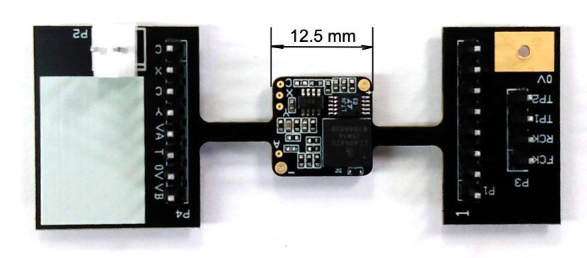
[07-JAN-22] Two versions of the A3028 electronic circuit are in active production today. We use the black A3028KV2 to make single- and dual-channel transmitters with the battery mounted on the top side of the circuit board. We use the red A3028PV2 to make single-channel transmitters with the battery mounted on the edge of the circuit board. The photographs below shows the A3028KV2.

Figure: Top Side of A3028KV2 Assembly, No Battery Loaded. The battery will mount on top of this side with the positive battery terminal facing the circuit board. Once the two necks are cut off, the circuit is 12.5 mm square. For bottom side see here.
The A3028PV2 provides a notch to accommodate side-mounting of a coin cell. The result is a transmitter that is long and thin, rather than the short and thick device produced when we mount the battery on top of the A3028KV2.

Figure: Top Side of A3028PV2 with 12.5-mm Diameter CR1225 Battery.
We modify the A3028 circuits several times a year, producing new versions with new names that use new components and require new firmware. Some modifications bring about slight improvements in performance. Most recent modifications we have been forced to make in order to work around shortages of semiconductors. We find parts that will permit construction of a transmitter then design and build a circuit around those parts.
| Version | Firmware
Folder | Source
Code | Programming
File | Comment |
|---|
| A3028KV1 | P3028C | P3028C01.abl | P3028K.xcf | Black, dual extensions, retired. |
| A3028KV2 | P3028C | P3028C01.abl | P3028K.xcf | Black, dual extensions, active. |
| A3028PV2 | P3028P | P3028P03.abl | P3028P.xcf | Red, single extension, C-antenna only, active. |
| A3028PV3 | P3028P | P3028P03.abl | P3028P.xcf | Red, single extension, C or D-antenna, coming soon |
Table: Firmware and Programming Files for Recent Circuit Assemblies.
The firmware directory exists only on our SCT calibration computer. The source file is the firmware file we edit and compile during SCT calibraiton. The programming file is the device programming configuration file we use to upload the firmware into the SCT logic chip.
Modifications
[23-MAY-22] We purchase boards fully-loaded with parts from our assembly house. We change various capacitors and resistors to create new versions of the assembly. The table below shows how we modify the A3028KV2 assembly to create most versions. We modify only those components that are necessary for the new version to function correctly. Some versions require more complex modificaitons, which we describe separately.
| Version | C7 | C8 | C9, C10, C11 | C12 | C13 | C14, C15, C16 |
|---|
| A3028A1 | same | same | 3.9 nF | same | same | 3.9 nF |
| A3028A2 | same | same | 2.0 nF | same | same | same |
| A3028A3 | same | same | same | same | same | 1.0 nF |
| A3028A3Z | 1.0 kΩ | 620 kΩ | same | 1.0 kΩ | 620 kΩ | 1.0 nF |
| A3028A4 | same | same | 510 pF | same | same | 510 pF |
| A3028A5 | same | same | 240 pF | same | same | 240 pF |
| A3028B3 | same | same | same | same | same | same |
| A3028C1 | same | same | same | same | same | 3.9 nF |
| A3028C2 | same | same | same | same | same | same |
| A3028D3 | same | same | same | same | same | 1.0 nF |
| A3028E3 | same | same | same | same | same | same |
| A3028H2 | same | same | 2.0 nF | same | same | same |
| A3028Q3 | same | same | same | same | same | 1.0 nF |
| A3028Q3 | same | same | same | same | same | 1.0 nF |
| A3028Q3Z | 1.0 kΩ | 620 kΩ | same | 1.0 kΩ | 620 kΩ | 1.0 nF |
| A3028Q4 | same | same | 510 pF | same | same | 510 pF |
| A3028W1 | same | same | 3.9 nF | same | same | 3.9 nF |
| A3028W1Z | 1.0 kΩ | 620 kΩ | 3.9 nF | 1.0 kΩ | 620 kΩ | 3.9 nF |
Table: Modifications to the A3028KV2 Assembly for Various Versions of A3028. Entries marked "same" mean no modification is required. For the locations of components see A3028KV2_Top and A3028KV2_Bottom.
The following table gives modifications to the A3028PV2 assembly to create the most versions.
| Version | C7 | C8 | C9, C10, C11 |
|---|
| A3028PV2 | same | same | same |
| A3028P1 | same | same | 3.9 nF |
| A3028P2 | same | same | same |
| A3028P3 | same | same | 1.0 nF |
| A3028T1 | same | same | 3.9 nF |
| A3028T2 | same | same | same |
| A3028T3 | same | same | 1.0 nF |
| A3028S1 | same | same | 3.9 nF |
| A3028S2 | same | same | same |
| A3028S3 | same | same | 1.0 nF |
| A3028S1Z | 1.0 kΩ | 620 kΩ | 3.9 nF |
| A3028S2Z | 1.0 kΩ | 620 kΩ | same |
| A3028S3Z | 1.0 kΩ | 620 kΩ | 1.0 nF |
Table: Modifications to the A3028PV2 Assembly for Various Versions of the A3028. Entries marked "same" mean no modification is required. For the locations of components see A3028PV2_Top and A3028PV2_Bottom.
If your version is not listed above, look for it in the paragraphse below.
A3028J3: The J3 is a combined EEG/EMG transmitters with four input leads. We start with the two-channel A3028KV2 circuit. We leave the X amplifier intact, but modify the Y amplifier on the top side. We remove C13, C14, and C16. We replace C12, R12, R13, and C15 with 2.0 MΩ. We replace R15 with 100 nF. We replace R16 and R18 with 50 kΩ. We load 510 pF for C18. We solder the green Y− lead to the pad of the C13 footprint that is connected to R13. The result is the S3028J differential amplifier, in which output Y is equal to 31 × (Y+ − Y−) with bandwidth 1-200 Hz.
A3028G3Z: The G3 is a combined EEG/EMG transmitter with four input leads and frequency response extending down to 0.0 Hz on both inputs. We start with the two-channel A3028KV2 circuit. We replace C7 and C8 with 50 kΩ on the bottom side. We now have X gain ×50 with bandwidth 0.0-160 Hz. Now modify the Y amplifier on the top side. We replace C12 and R13 with 620 kΩ. We replace R12 with 2.0 MΩ. We remove C13, C14, C15, and C16. We replace R15, R16, and R18 with 50 kΩ. We load 2.0 nF for C18. We solder the green Y− lead to the pad of the C13 footprint that is connected to R13. The result is the S3028G3Z differential amplifier (but with C18 = 2.0 nF), in which output Y is 100 × (Y+ − Y−) with bandwidth 0.0-50 Hz.
[19-JUL-23] Most dual-channel versions of the A3028 have three leads. On the circuit diagram, these are named X, Y, and C. They are red, yellow, and blue respectively. Single-channel versions omit either the red or yellow lead. The A3028P provides one input channel only. Its inputs are X and C, and the leads are red and blue.
| Name | Function | Comment |
|---|
| X | X positive input | Red, connected to VC by 100 nF in series with 10 MΩ |
| Y | Y positive input | Yellow, connected to VC by 100 nF in series with 10 MΩ. |
| C | shared negative input | Blue, connected directly to VC. |
| OUT | radio-frequency antenna | Clear, flexible steel antenna |
Table: Connections to Devices with 0.3 Hz High-Pass Filter. When we eliminate the high-pass filter, the 100 nF capacitor is replaced by 0 Ω.
The A3028J is an unusual dual-channel transmitter: it has four input leads. They are red, yellow, blue, and green. The two signals it transmits are Red − Blue and Yellow − Green. We discuss this unusual version later in this section
| Name | Function | Comment |
|---|
| X+ | X positive input | Red, connected to VC by 100 nF in series with 10 MΩ. |
| X− | X negative input | Blue, Connected directly to VC |
| Y+ | Y positive input | Yellow, connected to VC by 4 MΩ. |
| Y− | Y negative input | Green, connected to VC by 4 MΩ. |
| OUT | radio-frequency antenna | Clear flexible steel antenna |
Table: Connections to the A302J.
The A3028's on-board amplifiers and filters take the X and Y inputs and produce the XA and YA signals. The gain of the A3028A amplifiers is ×100, while Its high-pass filter provides a cut-off frequency of 0.3 Hz, and its low-pass filter provides a cut-off frequency of 160-Hz. The gain of the A3028AZ amplifiers, on the other hand, is ×10, with no high-pass filter, and a 160-Hz low-pass filter. In all versions of the A3028, XA and YA are applied to a sixteen-bit analog-to-digital converter (16-Bit ADC). In the A3028A and A3028AZ, the ADC samples XA and YA alternately at 512 SPS per channel, for a combined sample rate of 1024 SPS. In the A3028B, sampling from YA is disabled, and XA is sampled at 512 SPS. In the A3028C, sampling from XA is disabled, while YA is produced by a 0.3-40 Hz filter sampled at 128 SPS.

Figure: Epileptic EEG in Adult Mouse. Recorded with an A3028P providing 0.3-40 Hz and 128 SPS. Seizure provoked by picrotoxin.
The 16-bit ADC produces numerical values 0-65535, and these values are what we see plotted in the Receiver Instrument and Neuroplayer Tool. A value of 0 for means XA = 0V, and 65535 means XA = VBAT. A fresh lithium battery, such as the BR1225 in the A3028A, provides VBAT = 2.8 V during the first day of operation. With amplifier gain ×100, each sixteen-bit count represents 435 nV at the amplifier input. In the last few hours of a transmitter's life, VBAT drops to 2.2 V, at which point one ADC count is 350 nV. For most of the life of the transmitter, however, the battery voltage will be just below 2.7 V. When working with the A3028A, we assume a conversion factor of 400 nV/cnt. When we set the range of our signal plot to 5000 counts, this will be close to 2.0 mV. Consult the version table for the conversion factors other versions.
In theory, the dynamic range of the A3028A is 2.7 V ÷ 100 = 27 mV. But in practice, the amplifier is not able to drive XA all the way up to VBAT nor all the way down to 0 V. The actual dynamic range is closer to 24 mV. We specify a dynamic range that is 90% of the range we get when we multiply the sixteen-bit count conversion factor by 65536. Thus for the A3028AZ, with conversion factor 4.1 μV/cnt, the dynamic range is 90% of 270 mV = 240 mV.
Most versions of the A3028 provide a DC-blocking capacitor at each input. These are C7 and C12 in the schematic. Together with input resistors R5 and R12, they each form a high-pass filters with time constant 1.0 s. There is another high-pass filter in each amplifier, consisting of R6/C8 for X and R13/C13 for Y. In most versions of the A3028, these provide a time constant 0.5 s. The figure below shows the theoretical step response of the A3028A inputs, and compares it to that of other devices we have manufactured.

Figure: Step Response of A3028 and Other Circuits. The A3028 plot applies to any A3028 input with 0.3-Hz high-pass filter.
The common-mode reference voltage in the amplifier is VC, and VC is derived from the battery voltage by a 1.8-V regulator. Thus VC is 1.8 V, and the average value of both XA and YA are also 1.8 V. Thus the average digital value of X and Y correspond to 1.8 V. This allows us to calculate the battery voltage from the average value of either channel. We have VBAT = 65535 / Xave × 1.8 V, where Xave is the average value of X. This relation applies to all versions of the A3028, and both inputs, regardless of the gain and frequency response of its amplifiers, and regardless of what battery we have installed.
The figure below shows the X signal from an un-encapsulated A3028E as we reduce VBAT from 4.2 V to 1.2 V over 300 s. Our formula for VBAT from the average value of X works down to VBAT = 1.9 V. After that, the X decreases, suggesting an increase in VBAT, when in fact the actual VBAT drops to 1.8 V and the transmitter turns off.

Figure: X versus Time. We plot the sixteen bit value of X, with each vertical division being 6553.5 counts. Time is 15 s per division. Power supply voltage is 4.2 V on the left and 1.2 V on the right, so dropping 150 mV per horizontal division.
The analog input impedance of X and Y is 10 MΩ in the pass-band of the amplifier. Most versions of the A3028 provide a high-pass filter at 0.3 Hz to remove slowly-varying electrochemical potentials so that the gain of the amplifier can be ×100 and the dynamic range is the battery voltage divided by 100. The A3028's lithium primary battery provides 2.7 V for most of the operating life of the device, so the dynamic range is 27 mA. The A3028AZ amplifier, however operates all the way down to 0.0 Hz and accommodates electrochemical potentials by reducing the amplifier gain to ×10 so that the input dynamic range is 270 mV. Transmitters that are sensitive down to 0.0 Hz are able to record cortical spreading depressions (CSDs), as illustrated here.
We set the cut-off frequency of the A3028 three-pole, 3-dB ripple, Chebyshev, low-pass filters by our choice of filter capacitance, CF. Most often, we set the cut-off frequency at one third the sample rate. There are three capacitors in each filter that must have the same value for the filter to function properly. They are C9, C10, and C11 for the X filter and C14, C15, and C16 for the Y filter. With CF = 1.0 nF, the cut-off frequency is 160 Hz. The following graph shows how the gain of the two inputs of an A3028A varies with frequency.

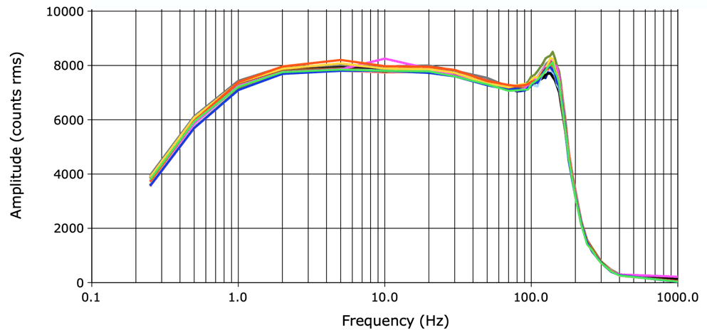
Figure: Frequency Response of a Batch of A3028C2. Stimulus is 30 mVpp sinusoid. Nominal bandwidth is 0.3-80 Hz.
The frequency response in the pass-band shows a slight decrease in gain from 10 Hz to 80 Hz, followed by a bump up at 130 Hz. These two features are the 3-dB ripple of the three-pole Chebyshev filter. By tolerating this non-uniformity of gain in the pass-band, we obtain a far sharper cut-off at the top of the pass-band. Amplitude drops by a factor of ten, or 20 dB from 160 Hz to 256 Hz. Frequencies above 256 Hz when sampled at 512 SPS will produce artificial sin-waves of lower frequency, in a process called aliasing. The purpose of our low-pass filter is to prevent aliasing. Even with the sharp cut-off of our Chebyshev filter, we might still see aliasing of high frequency components in EEG.

Figure: Aliasing of 500-Hz 10-mV Input for 512 SPS and 160-Hz Low-Pass Filter. We see 12 Hz of amplitude 200 μVpp.
The plot above shows how 10-mVpp of 500 Hz applied to the X input of an A3028A would appear after low-pass filtering and sampling. The signal has an apparent frequency of 12 Hz, which is 512 − 500. The EEG signal power decreases with frequency, so we can place our cut-off frequency at one third the sample rate and be confident we will see no significant distortion due to aliasing. The same is not true of EMG, in which the signal power density reaches a maximum somewhere between 100-300 Hz. When we record EMG at 512 SPS, we recommend placing the cut-off frequency at one sixth the sample rate, so that all EMG components above half the sample rate will be eliminated by the low-pass filter.
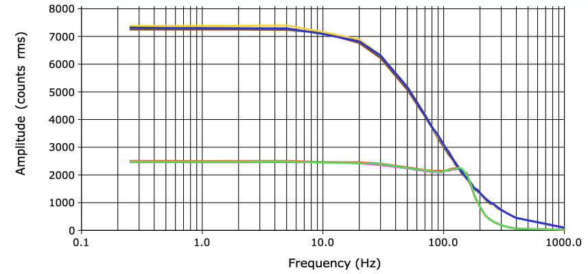
The A3028J provides a 0.3-160 Hz EEG input and a separate differential 1-200 Hz EMG input, both sampled at 512 SPS. These dual-channel transmitters come with four leads. We have X+ and X− for the EEG input, and we have Y+ and Y− for the EMG intput. The transmitter subtracts the positive and negative inputs to obtain the potential it digitizes and transmits. If we apply connect the Y inputs together and drive them with a sinusoiod with respect to the X−, we would like to see no signal at all on our Y voltage, since there is no difference between the two inputs. When we perform this experiment with a 30-mVpp 10-Hz sinusoid, we see 14 μVpp on Y.

Figure: Frequency Response of Two A3028Js. We apply a 16-mVpp sinusoidal sweep to the X and Y inputs and record the rms amplitude of the sixteen-bit transmitted signals. The X inputs, intended for EEG, have the higher gain and 0.3-160 Hz bandwidth. The Y inputs, intended for EMG, have the lower gain and the approximate 1-200 Hz bandwidth.
The A3028G3Z provides 0.0-160 Hz on its EEG inputs and 0.0-50 Hz on its EMG inputs. The "Z" in the part name means "Zero Hertz". Our Zero-Hertz transmitters have lower gain so that they can accommodate constant electrochemical potentials.

Figure: Frequency Response of a Batch of Dual-Channel A3028G3Z. Stimulus is 90 mVpp sinusoid. Nominal bandwidth 0.0-160 Hz for X input and 0.0-50 Hz for Y< inputs.
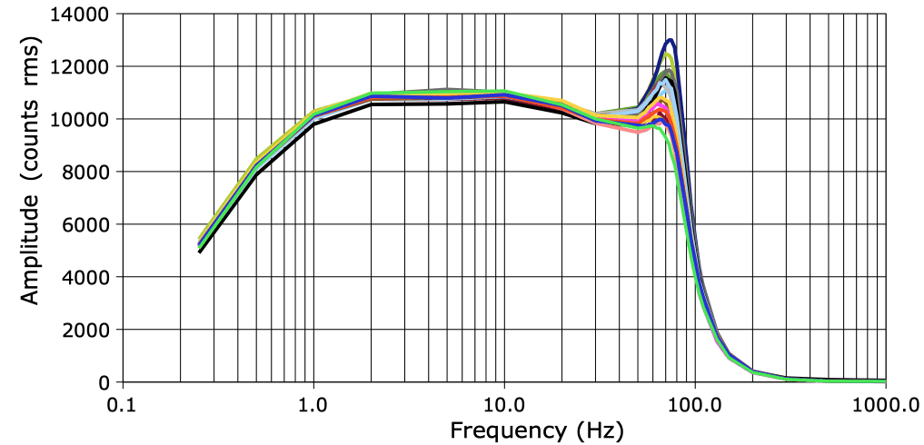
We expect some variation between amplifiers, because the three-pole filter is sensitive to the exact component values. The plot below shows the frequency response of a batch of fourteen A3028E transmitters stimulated with a 30-mV sinusoid through a 20 MΩ resistor.

Figure: Frequency Response of a Batch of A3028E3. Stimulus is 20 mVpp sinusoid. Nominal bandwidth 0.3-160 Hz.
At 10 Hz, the fourteen channels agree to within ±0.5 dB. At 130 Hz, where we have the bump in the Chebyshev response, they agree to within ±1 dB. These variations are well within the range we expect with 5% capacitors and 1% resistors.
An A3028 with two inputs, such as the A3028A or A3028D, provides two separated amplifiers for the X and Y signals. Both these signals use the same reference electrode C, which we call the common input. When we apply a signal to X, we would like Y to be unaffected. That is to say: when Y is connected to C, we would like the recorded value of Y to be zero regardless of the voltage we apply to X. We define the crosstalk from X to Y as the amplitude of Y divided by the amplitude of X when Y is connected to C. The crosstalk from Y to X we define in a similar manner. The crosstalk in the A3028 circuit is less than 2% and varies with frequency.

Figure: Illustration of Crosstalk from X (Green) to Y (Blue). We apply a 10-mV sinusoid of increasing frequency to X, and we leave Y connected to C.
The crosstalk reaches a maximum of 2% at 140 Hz, just below the cut-off frequency of the amplifiers. For 1-100 Hz, the crosstalk is 1%. Note that we have defined crosstalk in terms of a ratio of amplitudes, but it is more traditional to define it as a ratio of signal powers, or the ratio of the square of amplitudes, and then take the log to base ten and multiply by twenty to obtain the crosstalk in decibels. In these units, the A3028D crosstalk is −68 dB.
When we apply a pure sinusoidal waveform to the A3028, the sinusoid is amplified, filtered, digitized, transmitted, received, and recorded by the data receiver. The purpose of the A3028 is to provide high-fidelity EEG recordings, so we hope to see only a pure sinusoidal waveform emerge in the frequency spectrum of the recorded signal. We apply a 14-mVpp sinusoid of increasing frequency to the input of an A3028E transmitter providing 512 SPS and 0.3-160 Hz bandwidth. We measure the power of the recorded signal after subtracting its fundamental harmonic. This non-fundamental power is a combination of imperfection in the applied sinusoid, noise in the amplifier, and distortion in amplification and transmission of the signal. We divide the non-fundamental power by the total signal power to obtain a measure of the distortion of the sinusoid by the recording process.

Figure: Distortion in A3028 Recordings. We plot the ratio of non-fundamental power to total power for a sinusoidal input applied to a device with scattered sampling and another with uniform sampling. Most devices use scattered sampling to extend battery life.
By default, all transmitters take sample N+1 immediately after transmitting sample N, so the moment of sampling is displaced by the transmission scatter. When we reconstruct the signal for processing, we assume the samples are taken uniformly. Suppose we are looking at a 1-mVpp 10-Hz sine wave with a 512 SPS A3028E transmitter. The maximum slope of the sine wave maximum slope is 31 mV/s. The maximum displacement of the sampling instant is 240 μs. The maximum change from nominal to actual sampling instant is 240 μs × 31 mV/s = 7 μV. The diplacement of the sampling instants appears as noise of maximum value 7 μV and standard deviation roughly 4 μV. This is small compared to the A3028E's electronic noise of 12 μV rms. For a simulation of scatter noise, see here (by Marco Leite of ION/UCL). The spectrum of the sample-displacement noise, being random and independent from one sample to the next, is "white" or "flat with frequency". We call it scatter noise.
For the scattered-sampling devices, distortion remains less than 1% in the 0.3-160 Hz pass-band of the A3028 amplifier. At 10 Hz and below, distortion is less than 0.01%. The distortion power for scattered-sampling devices has a white noise spectrum: it is not distortion of the original sinusoid, but rather scatter noise that causes random distortion of the waveform. If we sample uniformly, we obtain the second plot shown above, in which distortion is less than 0.003%. With uniform sampling, the non-fundamental power is dominated by periodic signals that may be the result of distortion in the amplifier, or they may be imperfections in the signal produced by our function generator. The figures below show the spectrum of the non-fundamental power with uniform sampling.


Figure: Spectrum of Non-Fundamental Signal with Uniform Sampling From SCT with 0.3-160 Hz, 512 SPS, and 0.41 μV/cnt. Left: 5 Hz, 7-mV fundamental, 700 nV/div, 5 Hz/div. Right: 100 Hz, 7-mV fundamental, 700 nV/div, 25 Hz/div. Calculated from 8-s intervals with window function turned off. The peak that goes off the screen is the fundamental. Note the harmonics and offset harmonics.
Uniform sampling increases current by roughly 5%. In devices ×100 amplifiers (0.41 μV/cnt), scattered sampling does not introduce significant distortion of biopotential signals, and there is no practical reason to sample uniformly. But in devices with ×10 amplifiers, the distortion introduced by scattered sampling is more significant. All our zero-frequency devices, those with bandwidth extending down to 0.0 Hz, have ×10 gain (4.1 μV/cnt) so as to accommodated constant chemical potentials introduced by the metal interfaces in our signal path. For these devices, we enable uniform sampling.

Figure: Frequency Response of A3028AZ, X and Y, For 60-mVpp Sinusoid. The original name of the A3028AZ was the "A3028U".
The A3028AZ provides a 200-mV dynamic range and 0.0-160 Hz bandwidth on both inputs. Its EEG amplifier gain is only ×10, compared to our usual ×100. The A3028S2Z provides a single 0.0-80 Hz input with ×10 gain. Despite their low gain, the sixteen-bit resolution provides high-fidelity recording of seizures. The sensitivity to 0.0 Hz, combined with an X-Electrode bound by solderless crimp contacts, provides high-fidelity recordings of cortical spreading depresssions, provided we sample the signal uniformly.

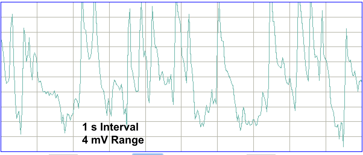
Figure: One-Second Interval of Kainic Acid Seizure Recorded with A3028S2Z and X-Electrode. From ION/UCL.
The least significant bit of the 16-bit digitized samples is 4.1 μV for battery voltage 2.7 V. We enable uniform sampling for all zero-frequency devices and total harmonic distortion remains less than 25 ppm (0.0025%) from 0.03 Hz to 160 Hz. In the case of the A30238WZ, the uniform sampling increases current consumptin from 48.5 μA to 50.4 μA.

Figure: Distortion in A3028AZ Recordings, Measured for Both Inputs. Operating band 0.0-160 Hz.
The figure below shows how the A3028E's 160-Hz low-pass filter responds to pulses applied to the X input.

Figure: Response of A3028E to 1-ms Pulses of 10 mV Delivered Through 50 Ω. The pulse frequency is 8 Hz. The vertical range is around 12 mV. For 5-ms pulses of 30 mV and 8 Hz delivered through 20 MΩ and the same vertical range, see here.
The low-pass filter introduces the ringing after the pulse, which consists of three maxima and minima in damped harmonic oscillation after the pulse has ended. The figure below shows the response of the A3028E to perforant pathway discharge spikes of amplitude roughly 10 mV.

Figure: Perforant Pathway Discharges, as Recorded with Wire Termination. The vertical range is around 12 mV.
The ringing we see after the discharge spikes is not generated by the brain itself, but rather by our low-pass filter. The slow, positive pulse following the negative spike is, however, produced by the brain, and the ringing is overlaid on top of this pulse.
Distortion of a sinusoidal signal applied to the input of one of our transmitters takes two forms. One is a white noise generated by scattered sampling of the signal, as we describe above. The power of this noise is less than 1% of the power of an applied sinusoid. The other is harmonic distortion and the introduction of periodic noise by the transmitter circuit. The power of these harmonics adds up to less than 0.003% of the power of an applied signal.
Our DC transmitters, which provide recording down to 0.0 Hz, are intended for recording slow-varying electrical phenomena such as cortical spreading depressions. The A3028U, for example, provides two 0.0-160 Hz recording inputs that allow us to observe a CSD moving across the brain. You will find example CSD recordings here, courtesy of ION/UCL. Our report on mains hum explains why our transmitters pick up no measurable mains hum when implanted in animals.
Synchronization
[22-AUG-21] When we want to mark in our SCT recordings the time at which some event took place, such as the start of a video recording, the moment that a light was flashed, or when an noise commenced, we can use an auxiliary SCT to record a synchronizing signal along with the signals received from implanted SCTs. Most often, the synchronizing signal will take the form of a TTL voltage, where the TTL low and high voltages used to mean ON and OFF. A TTL low-level is any voltage in the range 0.0-0.2 V, while a TTL high-level is any voltage in the range 2.4-5.0 V. The BNC to SCT Interface (A3028BSI) allows us to connect an SCT to a synchronizing signal with a BNC cable.

Figure: The BNC to SCT Interface (A3028BSI-B). This version is equipped with all eight spade clips, and is designed to measure the frequency response of four SCTs simultaneously during quality control. Four standoffs are common to all versions of the BSI, and allow us to place the interface on a metallic surface. The SCTs will rest on the yellow regions of the board, where their antennas can operate efficiently.
The A3028BSI provides up to eight spade clips to connect four single-channel or two dual-channel SCTs to the same input signal. When we want to incorporate a synchronizing signal into our recording, we will use only one pair of clips. The four pairs of clips permit us to measure the frequency response of four SCTs simultaneously, which is useful to us during quality control and throughout accelerated aging. The A3028BSI-A is intended for logic level synchronization. It provides attenuition of ×1000 so a 3.3-V logic transition will appear as a 3.3-mV step up or down at the SCT input. The BSI-A provides a time constant of 100 μs to remove unwanted high-frequency noise, while at the same time preserving 1-ms synchronization. Note that most SCTs have a 0.3-Hz high-pass filter on their input, so a step up comes out like this in the recorded signal, and a step down is the opposite. The average value of a high-pass filtered signal is zero.
| Version |
Input
Impedance |
Output
Impedance |
Attenuation
(Input/Output) |
R1, R2, R3, R4-R7, C1 |
Number
of Clips |
Application |
| A3028BSI-A |
10 kΩ |
10 kΩ |
1000 |
10K, 100K, 100R, 10K, 1u0 |
2 |
Logic Level Synchronization |
| A3028BSI-B |
51 Ω |
10 MΩ |
100 |
51R, 100K, 1K0, 10M, 100p |
8 |
Quad SCT Frequency Sweep Response |
Table: Versions of the SCT to BNC Interface (A3028BSI). Schematic with component names S3028Y. The input impedance is the impedance seen by the incoming signal at the BNC socket. The output impedance is the impedance in series with the attenuated input signal. The attenuition divides the input signal so that it may be viewed in full by the SCT input.
To set up logic level synchronization, we connect the synchronizing signal to the BNC socket on the interface. We are going to record the signal transmitted by an SCT sitting on the interface circuit board, so must receive the SCT signal with an antenna. One way to record the SCT signal is to place an antenna outside our Faraday enclosures and place the interface next to the antenna, so as to obtain reception of the SCT signal even in the presence of local interference. If we operate outside an enclosure, we must make sure that the antenna we use for the synchronizing SCT does not share a receiver input with an antenna inside a Faraday enclosure. An external antenna sharing a receiver input with an internal antenna will introduce interference into the Faraday enclosure, compromising reception within the enclosure. So we will need a dedicated receiver input for our synchronizing SCT signal. Another way to record the SCT signal is to place the interface in one of our Faraday enclosures, in which case we must bring the synchronizing signal into the enclosure with a coaxial feethrough. The one-to-one BNC feedthroughs we provide in the back of our bench-top enclosures will serve this purpose, but we may have to remove an antenna from the enclosure in order to free such a feedthrough. If we don't want to reduce the number of antennas in the bench-top enclosure, we can add another feedthrough to the back wall for the synchronizing signal. When we are recording in a Faraday canopy, our Eight-to-Four Coaxial Feedthroughs (A3039C) may not be used to carry a synchronizing logic level into the enclosure. Instead, we can either tape a single BNC feedthrough connector to the floor of the Faraday canopy, or we can use one port on an Eight-to-Eight Coaxial Feedthrough (A3039A).
To act as the synchronizing transmitter, we select an SCT that we do not intend to implant in an animal. We turn it on and connect the ends of its two leads to the two spade clips. If the ends of the leads have no termination, we remove insulation from the helical wire of the lead, and fasten the exposed wire into the spade clip. As the logic level changes, we will see steps up and down in the SCT recording, or order 4 mV.
[22-MAR-21] By input noise we mean the signal recorded by the transmitter when it is sitting stationary in water. The A3028 has three significant sources of input noise: soldered terminations, its magnetic sensor, and its amplifier input. If we use bare wire terminations, we eliminate the first source. If we choose the correct battery, we eliminate the second source. The figure below shows the noise spectrum of twelve A3028B-AA-B45-B transmitters sitting in 37°C water. Total noise in the band 0.3-160 Hz for these devices is 4-6 μV rms.

Figure: Input Noise of Twelve A3028B-AA-B45-B Transmitters in 37°C Water. Devices made with A3028HV1 circuit, introduced FEB-21, and CR1225AH battery, introduced MAR-21. Horizontal scale 25 Hz/div, vertical scale 200 nV/div. Spectrum obtained with 8-s interval.
If we make the same device with an inferior choice of battery, we see noise generated by the circuit's magnetic switch. The figure below shows the noise spectrum of ten A3028B-AA-B45-B transmitters manufactured in FEB-18 with our original mouse-transmitter battery.

Figure: Input Noise of Ten A3028B-AA Transmitters in 37°C Water. Devices made with the A3028GV1 circuit, introduced FEB-17, and BR1225 battery. Horizontal scale 20 Hz/div, vertical scale 400 nV/div. Spectrum obtained from an 8-second interval.
Currently, we make our P and S version transmitters with the A3028PV1 circuit and all others with the A3028HV1. Both are equipped with a magnetic sensor that turns itself on and off at 5 Hz. Switching noise, if present, will appear as a fundamental at 5 Hz accompanied by strong harmonics all the way up to 100 Hz. Provided we use the correct battery with either circuit

Figure: Input Noise of Twelve A3028P1-AA-C33-C Transmitters in 37°C Water. Devices made with A3028PV1 circuit, introduced FEB-18, and CR1025 battery. Horizontal scale 5 Hz/div, vertical scale is 200 nV/div. Spectrum obtained from a 32-second interval. Maximum total noise in 0.5-40 Hz is 3.5 μV rms.
Maximum total noise in 0.5-40 Hz for these A3028P1 devices is 3.5 μV rms. We see no sign of switching noise either, although we certainly do see switching noise when we equip this same circuit with the BR1225 battery.
[21-AUG-18] The total noise on each input in the plot above is 5±1 μV rms. The peaks near 20 Hz, along with their harmonics at 40 Hz and 60 Hz, are generated by the magnetic sensor on the A3028GV1 circuit board. This sensor turns itself on and off at roughly 20 Hz. We call these peaks switching noise. The switching noise amplitude is the amplitude of the largest harmonic of the switching frequency. In the above signal, the largest harmonic is the fundamental harmonic, and its amplitude is 3.2 μV. When we present measurements of input noise, we specify the version of the A3028 electronic circuit, the battery loaded on the circuit, and the type of termination at the end of the leads. The electronic circuit has evolved over the years, and the noise it generates has slowly reduced. The lower the source resistance of the battery, the lower the noise. Terminations with solder joints generate low-frequency noise.

Figure: Input Noise for Three A3028C-CC Transmitters in 37°C Water. Horizontal scale is 10 Hz/div. Vertical scale is 400 nV/div. Spectrum obtained from a 32-second interval. These devices were made with the A3028GV1 circuit and BR1225 battery, and M0.5 screw terminations. Total noise in 2-80 Hz is ≤6.5 μV.
Switching noise is proportional to the battery's source resistance. The magnetic sensor switches itself on and off to reduce its current consumption. It draws current when it is on, and this current causes a potential drop across the source resistance of the battery. The battery voltage on the board contains bursts of noise at the magnetic sensor switching frequency, and this noise makes its way into the amplifiers. Of all the batteries we use with our transmitters, the BR1225 has the highest source resistance and produces the highest switching noise amplitude. The figure below compares the source resistance of various batteries. We find that lithium primary cells have higher resistance when they are fresh, so we discharge them by 0.1% before measuring their source resistance.

Figure: Battery Resistance vs. Diameter for Various Battery Types. For resistance versus thickness see here. Li_BR: BR-series lithium primary cells from Panasonic. Li_CR: CR-series lithium primary cells from Panasonic. MnLi: ML-series rechargeable batteries. LiPo: lithium polymer rechargeable batteries. When the battery is rectangular, we use the geometric mean of its length and width for its diameter. Resistance measured after 0.1% discharge.
Earlier versions of the A3028B-AA circuit suffered from switching noise up to 12 μV, which was visible in the Fourier transform of 32-second intervals of baseline mouse EEG. The A3028GV1 circuit reduced switching noise by increasing the decoupling capacitance in parallel with the battery by a factor of four. Now we reject any

Figure: Switching Noise of A3028B-AA Transmitters made with A3028RV2 Circuit and BR1225 Battery. The A3028RV2 was in use until JAN-18. We plot the spectrum of an 8-s interval recorded with ten transmitters in a beaker of water at 37°C. The switching noise is the peaks around 20 Hz and their harmonics. Vertical scale is 800 nV/div. and horizontal is 25.6 Hz/div. The largest peak is 6 μV, which is the maximum value we accepted during quality control.
[28-MAY-19] When we equip the A3028 with gold-plated pins, we solder these pins to the ends of the stainless steel electrical leads. When we immerse these soler joints in water, they generate electrical potentials that we call chemical artifact, as we discuss in Chemical Artifact. Most of the power in chemical artifact is below 0.3 Hz, but the amplitude of the artifact above 0.3 Hz can be hundreds of microvolts. Our quality control procedure for each batch of transmitters is to soak them in water at room temperature for three days, remove them, measure their frequency response, and put them into water at 37°C to measure input noise. When we put transmitters with soldered terminations into water, we first scrub their solder joints with a brush, which greatly reduces the chemical artifact. When they are first immersed, we see input noise of 10-50 μV rms in the range 2.0-160 Hz. After a few minutes, the noise drops to below 12 μV rms. When we immerse a batch of transmitters with bare wire terminations, the input noise is immediately less than 12 μV rms, and after a few minutes is less than 8 μV rms.
[11-MAR-14] The A3028 leads pick up radio-frequency power from the antenna. If the blue lead is left open-circuit and the red and yellow leads are connected to some solid body, the blue lead acts like an antenna. The radio-frequency power it picks up is demodulated by parasitic diodes in the EEG amplifier. The result is noise visible on the EEG, as shown below. Its amplitude is roughly 100 μV rms. If you see such noise in an implanted transmitter, your blue lead has a broken conductor.

Figure: Broken C-Lead Noise. The broken lead is not connected to the animal body, and acts as a radio-frequency antenna.
[07-JUN-19] Here's how we can check if a wire is broken inside the silicone insulation of one of the leads. We put the ends of the leads in water, on top of an antenna, turn the transmitter on and examine its signal in the Neuroplayer Tool or Receiver Instrument. If the leads are intact, the amplitude of the noise on the signal should be less than 10 μV rms.

Figure: Measuring Input Noise with Lead Tips in Water. The transmitter is above a loop antenna that has had its mounting brackets removed, allowing the antenna disk to sit directly on our work bench. The noise we see at the inputs of this A3028A transmitter should be less than 25 cnt rms, which is 25 cnt × 0.4 μV/cnt = 10 μV rms.
[01-DEC-16] We take a two-channel A3028D made with the A3028RV1 circuit and BR2330 battery and put it in water at 40°C. We use 8-s recording intervals to measure the amplitude and frequency of the switching noise in each of the two input channels No3 and No4 as the water cooled to 19°C.

Figure: Switching Noise Amplitude and Frequency versus Temperature. The transmitter has two channels. No3 is on the bottom side of the circuit board along with the hall effect sensor that generates the noise. No4 is on the top side of the circuit board.
The frequency of the switching noise increases with temperature. We perform the same experiment with four transmitters at once, using this processor to calculate the rms amplitude of the fundamental harmonic of the switching noise. Each transmitter is made with the A3028RV1 circuit, but we have two different types of battery.

Figure: Switching Noise Amplitude versus Temperature. No3/4 is an A3028D with BR2330 battery, No5 is an A3028B with BR1225 using the Red input, No10 is an A3028C with BR1225 using the Yellow input, No13/14 is an A3028A using BR1225.
In No13/14 the noise is far greater in Red than in Yellow. But in No10 the noise is as large as any we have seen, and appears on the Yellow input. The noise in the transmitter equipped with the larger, lower-resistance BR2330 battery is an order of magnitude smaller. We touch the tip of a ×1 probe to the package of the Hall Effect Switch on a battery-powered, un-encapsulated transmitter. We see no sign of 20 Hz, certainly less than 200 μV.
[21-MAR-21] Loading the CR1225AH onto the A3028HV1 circuit results in no observable switching noise in the encapsulated transmitters. Total noise is never greater than 6 μV in 1-160 Hz with bare wire terminations.
Power Measurement
Suppose we want to know the root mean square amplitude of a biometric signal, or the mean square amplitude, but we do not need to know its exact shape. When we monitor electromyography (EMG), our chief interest may be the power of the signal, to determine if an animal is awake or asleep, rather than examining the fluctuations in the signal itself.
As we mention above, when we try to represent a continuous, time-varying signal as a sequence of discrete samples, we must make sure that the variation in the time-varying signal between the sample points approximates a straight line. When we plot the sampled signal, we are going to display it by drawing straight lines between the samples, so these straight lines are supposed to represent what the signal actually did between the samples. If the signal varies greatly between samples, we will not see this variation. Failing to see rapid variations between samples may not concern us, but rapid variations can, through sampling, look like much slower variations when we join the samples with lines. If we sample a 100-Hz signal at 48 SPS, for example, our straight-line reconstruction of the signal will be a 2-Hz sinusoid. This generation of slow variation from rapid variation is aliasing. To avoid aliasing, we must filter the signal we want to sample so that it contains no changes of direction between sample points. With a perfect low-pass filter, which has gain 1.0 up to frequency fc and 0.0 above fc, we can sample at 2fc and avoid aliasing. In practice, low-pass filters are not perfect, and avoiding aliasing is not quite sufficient to provide adequate representation. In the A3028, we sample at 3.2fc. Our low-pass filter gain drops by a factor of 10 from fc to 1.6fc. For example, in our 512 SPS transmitter for EEG, we filter at 160 Hz. The filter gain drops by a factor of ten from 160 Hz to 256 Hz.
But aliasing does not change the power of a signal, not unless we somehow miss all the powerful moments of a signal by a spectacularly unfortunate choice of sample instants. For an irregular signal like EMG, sampling at 16 SPS and taking the standard deviation of the samples, will give us a good measure of the EMG signal amplitude. Most EMG power is in the range 40-300 Hz, so we can high-pass filter at 30 Hz and low-pass filter at 320 Hz to separate the EMG from any artifacts that may be generated by our EMG pick-up electrodes, sample at 16 SPS and obtain EMG power at a cost of only 1.8 μA in current consumption. Thus the A3028V monitors EMG on Yellow input and EEG on Red input and has the same battery life as the single-channel A3028B EEG monitor.
Body Capacitance
For a discusion of body capacitance, see Body Capacitance in the A3019 manual.
Battery Life
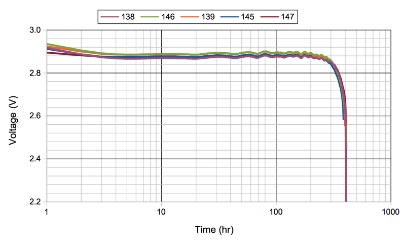
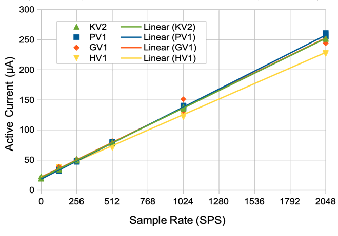
[30-SEP-21] The A3028 run down its battery sitting on the shelf in its inactive state and sampling and transmitting signals in its active state. The inactive current of the A3028 consists of the current consumption its magnetic sensor (U2) and its logic switch (U3). The shelf life of the transmitter is the time it takes the maximum inactive current to drain the battery. The maximum inactive current for temperatures −20°C to +80°C is 2.5 μA. At room temperature, the inactive current consumption of A3028 devices is only 0.8 μA. The A3028P1 battery has capacity 30-mAhr = 1250 μAdy, so its shelf life is 1562 dy = 52 mo = 4.3 yr. Transmitters equipped with larger batteries have shelf lives of decades, so we can leave them inactive for six months and lose less than five percent of their operating life.

Figure: Example Discharge Curves for Lithium Primary Batteries. We discharge five CR1025, 30-mAhr, 3-V cells with five A3028P3 transmitters, each consuming ≈75 μA. The batteries are connected with a wire soldered directly to the negative terminal and a solder joint directly on the positive terminal. Expected life is 400 hr, observed life is 391-410 hr. We measure VBAT by taking the average of one second's worth of the signal. The average value of the signal corresponds to VCOM, which is 1.8 V. From this we deduce VBAT, which corresponds to a sample value 65535.
The active current of the A3028 is its current consumption while transmitting its signal. This current depends upon the number of samples the transmitter takes per second. The A3028B provides one channel with 512 SPS. The active current consists of the quiescent current of the logic chip, which is independent of sample rate, and the consumption of the sample and transmit process, which increases linearly with sample rate. The figure below shows active current versus the total sample rate. To obtain the total sample rate, we add the sample rates of both channels.

Figure: Active Current versus Total Sample Rate for Various A3028 Circuits. We program the circuits with scattered sampling.
We have SCT circuits assembled in batches of one or two hundred at a time. Current consumption varies from one batch to the next as we buy new reels of parts to populate the boards. When we calculate the minimum operating life of an SCT, we use the following equation to obtain the maximum active current of the circuit when powered by a 2.7-V lithium primary cell.
Ia = 22 μA + (R × 0.12 μA/SPS)
We divide the nominal battery capacity by the maximum active current to obtain our minimum operating life. Yypical operating life is 10% higher. The following table presents minimum operating life for various batteries using the formula above.

Figure: Minimum Operating Life by Total Sample Rate and Battery Capacity.
Active current increases with battery voltage. The active current of an A3028 powered by a 3.7-V LiPo battery is 10% greater than that of the A3028 powered by a 2.7-V Li primary cell.

Figure: Active Current versus Battery Voltage for A3028Q. Total sample rate 2048 SPS.
The capacity of lithium primary cells decreases with active current and increases with temperature, as shown in the following plot taken from the BR1225 data sheet.

Figure: BR1225 Battery Capacity versus Load Current and Temperature.
The above plot suggests that a BR1225 battery delivering 250 μA at 15°C will provide 44 mAhr, or 176 hrs operation. Under these conditions, however, we observe closer to 190 mAhr, which implies the full 48 mAhr capacity.

Figure: Current Consumption versus Temperature for A3028P1. Sample rate 128 SPS.
Some transmitters implement a uniform sampling interval to reduce total harmonic distortion. These transmitters consume more current. To determine the maximum current consumption of a transmitter with uniform sampling, we use the following equation.
Ia = 22 μA + (R × 0.13 μA/SPS)
A typical A3028AZ provides uniform sampling at 1024 SPS and consumes 144 μA, while a typical A3028D provides scattered sampling at 1024 SPS and consumes 137 μA.
Encapsulation
[01-NOV-22] We encapsulate the A3028 in black epoxy and silicone. The outer layer of silicone is MED-6607, an unrestricted medical-grade silicone. The sensor leads are stainless steel springs coated with dyed silicone. The antenna is either a stranded stainless-steel wire coated with silicone, or a short sensor lead in the case of the smallest transmitter versions. We remove one in ten transmitters from our production line for accelerated aging. These transmitters run until they exhaust their batteries while fully immersed in water at 60°C or 80°C.
Corrosion causes the failures of electronic circuits in warm, humid environments. Both silicone and epoxy are permeable to water vapor. An implanted transmitter encapsulation becomes saturated with water vapor. Occasional drops in temperature cause condensation in any cavities that may exist within the transmitter, such as within a cracked ceramic capacitor or beneath a surface-mount component. Condensed water, the warmth of the animal body, flux residue, and electrical voltages combine to promote corrosion that leads initially to loss of performance in the EEG amplifier and ultimately to premature draining of the battery. At 60°C, corrosion occurs over ten times faster than at 37°C in an animal body.
We guarantee our transmitters against failure from corrosion while implanted. Our encapsulation procedure seeks to remove flux residue by repeated washing and scrubbing in hot water, and to eliminate cavities in the epoxy by use of vacuum and atmospheric pressure. The minimum operating life of an encapsulated A3028RV3 circuit in 100% humidity at 60°C is 100 days, with the first artifacts of corrosion appearing in the EEG signal after 50 days. Implanted in an animal, we expect no sign of corrosion in the EEG for 500 days, and no failure through corrosion for 1000 days. None of the popular versions of the A3028A run for 500 days. The A3028GV1 circuit we have just introduced for use in mouse transmitters. We poached ten devices at 80°C. Two stopped transmitting after 6 days, which is equivalent to 360 days implanted, and the remaining 8 lasted 13-14 days, which is their full operating life, and equivalent to 780 days implanted. Looking at our notes we find that we did not clean these circuits a second time before encapsulating, so we suspect the two early failures were caused by flux residue and moisture. But in any case, none of our mouse transmitters run for more than 100 days implanted, so we have no fear that these will fail prematurely by corrosion.
Development
We have moved our development to a separate page, Subcutaneous Transmitter Development.

