Subcutaneous Transmitter (A3019)
© 2010-2014, Kevan Hashemi,
Open Source Instruments Inc.
Contents
Description
Design
Analog Inputs
Input Noise
Body Capacitance
Battery Life
Encapsulation
Example Recordings
Modifications
Development
Description
The Subcutaneous Transmitter (A3019) is an implantable telemetric sensor for monitoring EEG. It succeeds the Subcutaneous Transmitter (A3013), being a smaller implementation of an almost identical circuit. See Subcutaneous Transmitter System for an overview of the transmitters and data-acquisition.

Figure: Subcutaneous Transmitter A3019A with Screw Electrodes. This transmitter is designed for use in mice. Volume is 1.4 ml, width 13.5 mm. Operating life is 4 wks at 512 SPS. All wires are 316 stainless steel. The antenna is stranded wire coated with silicone. The leads are helical wire insulated with silicone. The silicone is dyed red for the X+ lead and blue for the X− lead. The screws are M0.5, 1-mm long with binding heads. The mass of the entire device is 2.6 g.
The A3019 comes with two helical stainless-steel leads coated with silicone. When the leads are insulated with colored silicone, as they are in the photograph above, you cannot see the helical wires within the insulation. But you can see the helical wires in this photograph of an older A3019A with clear insulation. The X+ and X− leads detect a single biopotential, such as EEG. The transmitter is equipped with a 50-mm stranded, stainless-steel silicone-insulated antenna. Depending upon the application, the user may prefer bare wire termination on the X+ and X− leads, or screws that suit the thickness of the animal skull and the duration of the experiment. We discuss the various options for electrodes on the tips of the leads in Electrodes. We discuss how we can use two electrodes to measure brain potential in The Source of EEG.
| Property | Value |
|---|
| Volume (Body Only) | 1.4 ml |
| Mass (Entire Device) | 2.6 g |
| Outer Dimensions | 13.5 mm × 13.5 mm × 8.0 mm |
| Operating Life | 4 wks |
| Shelf Life | 60 wks |
| Number of Inputs | 1 |
| Type of Input | Differential |
| Input Impedance | 10 MΩ || 2 pF |
| Samples Per Second | 512 |
| Sample Resolution | 16-bit |
| Input Dynamic Range | 20 mV |
| Input Bandwidth | 0.7 Hz − 160 Hz |
| Input Noise | 12 μV |
| Input Mains Hum | <1 μV |
Table: Specifications of the A3019A.
The A3019D is the same as the A3019A, but with a larger battery mounted beneath it. Half the volume of the A3019A is taken up with its 48 mA-hr battery. Three quarters of the volume of the A3019D is taken up with its 225 mA-hr battery. The larger battery allows a more efficient encapsulation process, so we take up less volume with epoxy. The result is an unattractive but long-lasting transmitter.

Figure: Subcutaneous Transmitter A3019D with Screw and Bare Electrodes. Ruler divisions on the right are in millimeters. This transmitter is designed for use in adult rats. All the leads are insulated with five coates of silicone, while the body is insulated with eight coats. Volume is 2.4 ml, diameter 23 mm. Operating life is a minimum of 16 wks at 512 SPS. The orange lead is X+, with a bare steel helical termination for insertion into a skull hole. The green lead is X− with a screw electrode. The screw has a binding head over a 1.6-mm diameter, 3.2-mm long thread. The antenna is stranded stainless steel. The mass of the entire device is 6.5 g.
We determine the version of a transmitter during assembly, programming, and encapsulation. We might change capacitors on the board to set the filter frequencies. We might change resistors to set the gain. We program the logic chip to set the sample rate for each channel. We can equip the circuit with a small, medium, or large battery. The larger the battery the longer the operating life of the transmitter, but the greater its volume. The following table gives the versions of the A3019A that we have defined to date. Click on the version names to see pictures of the individual versions, should they exist.
Function
Code |
X |
Battery
Capacity
(mA-hr) |
Volume
(ml) |
Width
(mm) |
Height
(mm) |
Operating
Life
(weeks) |
Shelf
Life
(weeks) |
| A3019A |
20-mV range, 0.7-Hz HPF,
160-Hz 3-pole LPF, 512 SPS |
48 |
1.4 |
13.5 |
8.0 |
3.6 |
60 |
| A3019B |
20-mV range, 0.7-Hz HPF,
160-Hz 3-pole LPF, 512 SPS |
120 |
1.8 |
∅18 |
7.0 |
9 |
150 |
| A3019C |
20-mV range, 0.7-Hz HPF,
160-Hz 3-pole LPF, 512 SPS |
160 |
2.2 |
∅24 |
7.4 |
12 |
190 |
| A3019D |
20-mV range, 0.7-Hz HPF,
160-Hz 3-pole LPF, 512 SPS |
255 |
2.8 |
∅23 |
8.0 |
18 |
300 |
| A3019E |
20-mV range, 0.7-Hz HPF,
160-Hz 3-pole LPF, 512 SPS |
1000 |
5.0 |
∅25 |
12.7 |
70 |
1200 |
| A3019F |
20-mV range, 0.7-Hz HPF,
720-Hz 3-pole LPF, 2048 SPS |
255 |
2.4 |
∅23 |
7.0 |
6 |
300 |
| A3019P |
20-mV range, 0.7-Hz HPF,
160-Hz 3-pole LPF, 512 SPS |
none |
0.4 |
12.0 |
3.0 |
none |
none |
Table: Version Letters for the A3019. We use LPF for Low-Pass Filter, HPF for High-Pass Filter, and SPS for Samples Per Second. We give typical values for battery life and volume. We measure volume by water displacement. When thickness varies, we give the average thickness.
The A3019F uses 220 pF capacitors in its low-pass filter instead of the 1 nF capacitors used by the A3019D. The result is a three-pole low-pass filter with a cut-off frequency of 720 Hz. The A3019F is programmed to sample and transmit at 2048 SPS. The low-pass filter provides 17 dB of attenuation at 1 kHz and 30 dB of attenuation at 1.5 kHz. At Outwardly, the A3019F is identical to the A3019D. Although it samples at four times the rate of the A3019D and uses the same battery, its operating life is only three times shorter. A component of the operating current of the A3019D is independent of sample rate, and this component remains the same in the A3019F.
Versions C and D look the same from above, but the C version uses a slightly thinner battery, for a maximum height of 6.4 mm instead of 7.0 mm. For comparison, the A3013A, which we implanted in dozens of rats with success, was 17 mm × 19 mm × 10 mm. Its volume without its antenna or leads was 2.4 ml.
By default, the transmitters come with eight coats of silicone. The average build depth per coat is 100 μm, so eight coats produces a skin of 0.8 mm of silicone. This thickness has proved rugged enough to withstand the claws of rats. The scratch marks penetrate the silicone by half a millimeter, but do not pass through.
It turns out that clear and white leads blend in well with animal tissue, making it hard to spot the leads when removing a transmitter from an animal for re-use. By adding dye to the silicone of the leads, we can provide colored leads. We have so far used red, orange, yellow, green, blue, and purple dyes with success. To identify the transmitter channel number, we add a sticker beneath the final few layers of silicone. The transmitter above shows an example of such a sticker, as well as colored leads.
Design
S3019_1.gif: Subcutaneous Transmitter Circuit Diagram.
Code: Logic Chip Firmware Library.
A301901B.zip: Version B PCB Gerber Files.
A301901B_Panel.zip: PCB 2×5 Panel Gerber Files.
A3019A.xls: BOM, PIK, KIT, and Cost for A3019A Production.
R3019.ods: Calibration currents and battery dates (ods spreadsheet).
B22260_SMT.pdf: Component placement drawing from Advanced Assembly.
B22260_KitLab.pdf: Kit labels from Advanced Assembly.
B22260_AB.pdf: Parts list from Advanced Assembly.
The two input leads are X+ and X−. The antenna is OUT. You can see all three signals declared with these names in the circuit diagram. These are the only three connections we make to the circuit. The antenna is insulated from the outside world by a silicone tube. It transmits the value of X with radio waves. The leads can be various colors, as requested by the user.
| Name | Function | Comment |
|---|
| X+ | X positive input | Connected to VCOM by 100 nF in series with 10 MΩ.
Recommended for signal input. |
| X− | X negative input | Connected directly to VCOM.
Recommended for ground or reference input. |
| OUT | radio-frequency antenna | a flexible wire |
Table: Connections to the A3013.
The A3019 amplifies and filters X to produce a signal XA which passes into a sixteen-bit ADC. The result is a sixteen-bit number. The number is 0 when XA = 0 V and 65535 when XA = VBAT, the battery voltage. With a fresh battery, we have VBAT = 2.7 V. The A3019A has gain 100 in their amplifier, so we see that each ADC count represents roughly 400 nV at the X input. In the last few days of a transmitter's life, the VBAT drops to 2.2 V, at which point the transmitter fails. During this time, the voltage represented by each ADC count drops in proportion to the battery voltage. When VBAT is 2.2 V, one count represents roughly 350 nV.
Aside: By comparison, one ADC count in the earlier A3013A transmitter represented 140 nV at the X input. The gain of the A3091A is three times greater than that of the A3013A.
In theory, the dynamic range of the A3019A is 2.7 V ÷ 100 = 27 mV. But in practice, the amplifier is not able to drive XA all the way up to VBAT or all the way down to 0 V. So we quote the dynamic range as a more conservative 20 mV, or if we want to be more specific, −14 mV to +6 mV.
We discuss the noise present on the X input in our presentation of the A3020 prototype circuit here. With gain of 100, we expect less than 30 counts of noise in a 160-Hz bandwidth, which is 12 μV.
Like the A3013, the A3019 provides a DC-blocking filter on the X input as soon as it enters the circuit. The average value of XA is VCOM, which is 1.8 V. Thus the average value of the digitized signal corresponds to 1.8 V, and from this we can deduce the current value of VBAT. We used the average value of X to monitor battery voltage in the A3013. The same calculations apply to the A3019, regardless of the gain of its amplifiers.
The impedance between X+ and X− is 10 MΩ in series with 100 nF. The antenna makes no low-frequency connection with the outside world. It transmits radio-frequency waves out through its silicone sheath. The X input is isolated in that its associated amplifiers are not connected to the outside world at all, except through the capacitance between the transmitter battery and the animal body, which is a few tens of picofarads.
The A3019's analog filters and amplifier are similar to those of the A3013, which we describe in detail here. The principle difference between the two circuits lies in the elimination of one of the three op-amps used in the A3013 to arrive at a more compact circuit for the A3019. The input impedance of the two circuits is identical: 10 MΩ in series with 100 nF. But in the case of the A3019, the high-pass filter is dominated by the combination of R10 and C9. With 50 kΩ and 4.7 μF, the half-power frequency of this single-pole high-pass filter is 0.68 Hz.
Resistor R10 also sets the gain of the amplifiers, as shown by a table in the schematic. With R10 = 50 kΩ, the gain is 100. With R10 = 100 kΩ, the gain is 50 and the high-pass filter frequency drops to 0.34 Hz.
The A3019's three-pole low-pass filter circuit is identical to that of the A3013A. The following graph shows the measured response of this low-pass filter with frequency for various cut-off frequencies. We set the cut-off frequency by our choice of the filter capacitor value CF, as shown in the table in the schematic.

Figure: Frequency Response of Low-Pass Filter. We apply a 1-mV amplitude sine wave of increasing frequency to the input and record the rms ADC output in ADC counts.
The plots are normalized with respect to the response at 0.5 Hz in the presence of a high-pass filter with half-power frequency 0.17 Hz. When we make the same measurements for the A3019A circuit, we see the high-pass filter affecting the response below 1 Hz. The following graph shows the measured gain from X to XA through the A3019A amplifiers and filters combined. We obtained the gain measurement with our prototype board, not with an encapsulated transmitter.
Figure: Measured Frequency Response of A3019A amplifier and filters.
The following graph shows the frequency response of a selection of encapsulated A3019D transmitters. We connected a 30-mV p-p sin wave through two 10-MΩ to the two 150-mm X leads, so that one resistor was in series with each lead. We expect the amplitude at the input to the transmitters's amplifier to be 10 mV p-p once we get above the half-power frequency of our high-pass filter. With an amplifier gain of 100 and a battery voltage of 2.7 V, a 10 mV p-p signal of around 20 Hz should arrive at the ADC as a 1 V p-p signal, producing a digitized signal of amplitude 24300 counts p-p, or 8580 counts rms. What we plot below is the rms amplitude in ADC counts versus frequency.

Figure: Frequency Response of Encapsulated A3019Ds. A 30-mV p-p sinusoid is connected through two 10 MΩ resistors to the X leads.
We see variation in the frequency response from one transmitter to the next, which we assume is the result of variation in the resistor and capacitor values loaded on each circuit. Nevertheless, gain variation in the pass-band 2 Hz to 160 Hz is less than 2 dB, which is better than our target of 3 dB.
Figure: Frequency Response of A3019F. A 30-mV p-p sinusoid is connected through two 10 MΩ resistors to the X leads. Graph 4A is for transmitter No4 before encapsulation, and Graph 4 is after encapsulation.
The increase in the gain of transmitter 4 after encapsulation is due to the change in battery voltage. Before encapsulation, we provided 3.0 V power. Afterwards, the power is 2.7 V. With the smaller battery voltage, the dynamic range of the ADC is smaller in proportion, so the signal appears larger in ADC counts.
The cut-off frequency of the A3019F is roughly 700 Hz. The designed value is 720 Hz. At high frequencies, the above measurement does not drop to zero because the noise picked up by the 700-Hz bandwidth in our measurement fixture is significant. When we short the two input leads of an A3019F we observe noise of around 50 counts rms, which is twice the amplitude and four times the power of the noise we observe on the A3019D. This is as we expect: the A3019F has four times the bandwidth.
[20-NOV-12] When we turn on a transmitter and place it on a wooden table, what we will most likely see is mains hum, which is electrical potential induced between the input electrodes due to the electrical and magnetic fields created by alternating-current power in the walls and power cords of our laboratory. Its frequency will be 50 Hz or 60 Hz, depending upon where you are. If we connect the electrodes together, or place the transmitter in a faraday enclosure, the mains hum will disappear, leaving other kinds of noise that are generated by the trasmitter itself.
[06-MAY-11] With electrodes shorted together, or when immersed in pure water, most A3019As generate 12 μV of noise in their 160-Hz pass-band. The following table gives the amplitude of the 2-20 Hz and 60-160 Hz bands for fourteen A3019D transmitters in cool and warm water. We measured noise in salty water and pure water and found that the addition of salt had no effect. The table includes the baseline EEG amplitude we obtain from these same bands using eight transmitters implanted in control animals, as we describe here.
| ID
| Cool Water
Amplitude
2-20 Hz (uV) |
Cool Water
Amplitude
60-160 Hz (uV) |
Warm Water
Amplitude
2-20 Hz (uV) |
Warm Water
Amplitude
60-160 Hz (uV) |
| EEG | 22.7 | 11.5 | 22.7 | 11.5 |
| 5.1 | 13.1 | 8.4 | 6.0 | 6.9 |
| 5.2 | 4.4 | 8.0 | 5.0 | 7.2 |
| 5.3 | 7.3 | 7.6 | 5.2 | 6.6 |
| 5.4 | 13.9 | 6.9 | 6.8 | 6.7 |
| 5.5 | 6.7 | 7.1 | 5.9 | 7.0 |
| 5.6 | 5.9 | 12.1 | 7.4 | 7.1 |
| 5.7 | 6.0 | 7.4 | 7.4 | 7.4 |
| 5.8 | 4.7 | 7.6 | 8.0 | 7.3 |
| 5.9 | 6.6 | 7.1 | 9.8 | 7.1 |
| 5.10 | 8.1 | 16.1 | 4.8 | 6.8 |
| 5.11 | 3.9 | 7.3 | 5.7 | 6.0 |
| 5.12 | 5.6 | 8.5 | 7.7 | 7.2 |
| 5.13 | 5.4 | 9.0 | 8.6 | 7.0 |
| 4.14 | 5.1 | 8.5 | 6.3 | 8.6 |
Table: Noise Amplitude Compared to EEG Baseline. Transmitters in cool water (18°C) and warm water (32°C).
In cool water, noise power is three or four times lower than baseline 2-20 Hz EEG power. In the 60-160 Hz band, 5.6 and 5.10 produce significantly more noise power than baseline EEG. In warm water, however, the noise power drops to the levels we are accustomed to observing for unencapsulated circuits with their inputs connected together.
In cool water, 5.10 has a 5-μV peak at 18.5 Hz, as you can see here. In warm water, this peak disappears, as you can see here. The Hall Effect switch on the A3019 reduces its power consumption by turning itself on for a short interval roughly 17 times a second. We suspect this peak is caused by the switching of the sensor, and we call it switching noise. For plots of switching noise versus temperature, see below. We observe switching noise only in circuits with their batteries loaded.
[08-MAY-11] Further experiments show the switching noise arising for temperatures below 25°C, with the 5.10 peak reaching a maximum amplitude of 9 μV at 15°C, and decreasing for lower temperatures. The A1171 Hall Effect Switch (U1) uses an internal switching frequency of 200 kHz to obtain a measurement of local magnetic field strength roughly 17 times a second. The noise we observe is present even when the input to our amplifier is shorted. Its amplitude falls off above 160 Hz. If we assume a capacitance between the switching voltage and a 1-MΩ resistor in the amplifier, and we assume switching of 2.7-V at 200 kHz within U1, we expect the noise across the resistor to be 1 mV/fF. Any non-linearity in the first stage of amplification at 200 kHz will demodulate the switching frequency, giving us noise at roughly 17 Hz.
The switching noise of each transmitter reaches a maximum at a temperature between 10-30°C, which suggests that the noise is the product of two phenomena, one of which becomes stronger with temperature, and the other weaker. The permittivity of epxoy increases with temperature. The demodulation of a 7-mV, 200 kHz signal will take place within the non-linear elements of the op-amp. The efficiency of such demodulation could be a decreasing function of temperature, but we have no argument for why it should be a function of temperature at all. In the long run, we would like to understand and eliminate switching noise from our transmitter amplifiers, but in the past six years we have made no progress in this endeavor. All we do is measure the switching noise and reject transmitters for which the noise is greater than 8 μV at 37°C.
[21-FEB-14] We observe in three implanted transmitters (29.1, 29.6, 29.10) at ION noise that is characteristic of a damaged RF oscillator. Such damage occurs when we touch the antenna with a metal tool while the transmitter is active. We first encountered this damage in the A3013X. The signal and spectrum here is from No29.6 while implanted. Its amplitude is around 100 μV rms and its spectrum peaks at 125 Hz. The only way to be sure that this is noise resulting from antenna damage is to check to see if VBAT is connected to the antenna. We will do this when we get the transmitters back from Aytakin.
[22-FEB-14] We see another form of noise on transmitter No29.11 implanted at ION, as shown here. There is a peak at 80 Hz and baseline swings.
Body Capacitance
[03-AUG-12] We use X+ or X− as as a differential input. If you have a ground potential and an EEG potential, you can use either input as your ground most of the time. But if you want to monitor the signals inside individual neurons, you had best use X+. You never need a third wire for a low-impedance ground. Indeed, there is nowhere to connect a third wire, and any effort to add such a connection would undermine the sensitivity of the X input.
The X− input is connected to the VCOM power supply. When biometric voltage source moves the electric potential of X− up and down, the potential of the transmitter circuit and its battery moves up and down also. If VCOM goes up by 1 mV, so do the VBAT, 0V, and 1V8 voltages in the circuit. The charge the voltage source must push into the transmitter to change its potential by voltage V is equal to CV, where C is the electrical capacitance between the transmitter circuit and the animal body, which we call the transmitter's body capacitance.
The capacitance between two parallel conducting plates, each of area A, and separated by an isulating material of thickness d, is Aε/d, where ε is the permittivity of the insulator. Consider the A3019D with its 25-mm diameter battery. The battery surface is one plate of a capacitor, the epoxy and silicone of the encapsulation are the insulating material, and the animal tissue in contact with the encapsulation is the other plate of the capacitor. The epoxy and silicone have combined thickness of roughly 500 μm and have permittivity roughly 40 pF/m. Thus the capacitance between the battery and the animal tissue is roughly 40 pF. The capacitance between the top side of the battery and the animal tissue will be half as great because the encapsulation is twice as thick on the top. So the total capacitance between the A3019D circuit and the animal's body will be of order 60 pF. For the A3019A, the same estimate arrives at 15 pF.
[02-MAY-13] We place an A3019A transmitter in a faraday enclosure. We supply it with a 30-mV amplitude sine wave through two alligator clips. In series with each alligator clip is a 10-MΩ resistor. We place the electrode screws, on the end of their 45-mm leads, in the clips. We vary the sine wave frequency frm 10 Hz to 150 Hz and measure the amplitude of X as we observe it in the Receiver Instrument. Now we wrap the transmitter body in aluminum tape. We disconnect our clip from X− and connect it to the tape instead. Now we have the body capacitance of the A3019A in series with the clip as well. We vary the frequency from 10 Hz to 150 Hz. We obtain the graph below, which shows the relative amplitude of X with and without the body capacitance in series with the applied voltage.
Figure: Observation of Transmitter Body Capacitance. The plot the gain of the transmitter when supplied with a signal through its body capacitance and 20 MΩ, relative to the gain when the signal is supplied by 20 MΩ alone. The curve is the relative gain we expect for a 12-pF body capacitance.
On the same plot we show the relative gain we expect for an ideal 12-pF body capacitance. The agreement between these two curves suggests the body capacitance of the A3019A is of order 12 pF, which is consistent with our estimate of 15 pF.
[03-AUG-12] The X+ input is connected to the inverting input of an op-amp. The capacitance to ground at this input is 2 pF. The capacitance between X+ and ground is 2 pF in series with the transmitter's body capacitance, which is much larger than 2 pF. So the X+ input capacitance is 2 pF for all versions of the A3019.
But the encapsulated body of the transmitter is not the only source of capacitance between the transmitter circuit and the animal body. The two 150-mm leads of the A3019D add their own capacitance. The conductors in these leads are helical, but if we assumed they were solid wires 400 μm in diameter enclosed in silicone 700 μm in diameter, we conclude that the capacitance between each lead and the animal body fluid is roughly 110 pF.
Figure: Capacitance of Transmitter Leads.
The A3019A has 50-mm leads. The capacitance of its X+ input will be roughly 40 pF, and that of X− will be 55 pF. But the A3019D with 150-mm leads has X+ capacitance 110 pF and X− capacitance 170 pF. Of course, all our estimates are crude. For the rest of our discussion, we'll use 100 pF for both leads just to keep things simple.
Suppose we connect X+ directly into the soma of a neuron with a tiny, low-impedance probe, and X− into the extracellular fluid immediately outside the soma. When the neuron activates, charge flows into the soma from from the extracellular fluid. In order to raise the potential of the X+ input, some of this charge must flow into the 100-pF capacitance that exists between the X+ input and the body's ground potential. Even in the absence of the probe, the charge will have to fill up the membrane capacitance of the soma.
In The Source of EEG, we estimate the total membrane capacitance of a rat cortical neuron to be 200 pF. To the first approximation, the insertion of a probe connected to our transmitter would reduce the local action potential significantly. Because of its long and substantial electrode leads, the A3019A and A3019D are not suitable for recording intracellular signals. They are, however, well-suited to recording extracellular signals, and could certainly detect the extracellular activation potential of a single neuron.
Battery Life
The A3019 contains an A1171 hall sensor switch, U1 in the schematic, and an SN74AUP1G80 D-type latch, U2 in the schematic, to turn on and off power to the transmitter when we apply a magnetic field. The switch and latch together consume 5 μA from the battery at all times. Thus the inactive quiescent current of all versions of the A3019 is 5 μA.
The shelf life of a transmitter is the length of time it can sit inactive on the shelf before its battery is exhausted by the inactive quiescent current. With a 48 mA-hr battery, such as the BR1225 used in the A3019A, the shelf life is 9600 hours, or 57 weeks. With a 255 mA-hr battery, such as the BR2330 used in the A3019D, the shelf life is six years. In this respect, the A3019 is very much superior to the A3013, whose inactive quiescent current was around 22 μA. Indeed, the A3019A transmitter would not be practical with a 22-μA inactive current.
The active current consumption of the A3019 consists of the quiescent current of the logic chip, which is independent of sample rate, and current consumption of the sample and transmit process, which increases linearly with sample rate. We studied the current consumption of the A3019 with the help of the A3020 test board, as we describe here.
After assembling twenty A3019As, we arrive at the following empirical formula relating the active current consumption to the sample rate, M. The formula agrees with our observation that the active current consumption is, on average, 80 μA, with a standard deviation of 4 μm.
Iactive = 24 μA + (M × 0.11 μA)
The operating life of a transmitter is the length of time it can run before its battery is exhausted, assuming it started with a fresh battery. With a 48 mA-hr battery, the operating life of a 512 SPS transmitter is 3.6 weeks. With a 255 mA-hr battery, the operating life is 19 weeks.
[31-OCT-13] At ION, Rob Wykes has two A3019Ds that have been running continuously in two rats since 06-AUG-13 and 09-AUG-13. Expected operating life for the A3019D is 126 days. The animals are healthy, with no sign of problems with the transmitter or its antenna and leads. He has an A3019A, No23.1, that sat on the shelf from 03-JUN-13 to 08-OCT-13 and then ran continuously until 28-OCT-13, when it exhausted its battery. That's four months on the shelf and twenty days operating. Each month on the shelf uses two days of operating life, so we see that the total use was equivalent to 28 operating days. Our expected life for the A3019A is 26 days. The mouse with the transmitter is healthy and active.
Encapsulation
Warning: The A3019 circuit board is only 0.8 mm thick. We must take great care not to flex it when breaking it out of its panels, soldering wires to it, and cleaning it. If we bend it, capacitors and resistors on the board are likely to break. The danger of flexing it greatest when the programming extension is still attached.
[03-APR-14] Below you will find a description of our encapsulation procedure before we discovered the problem with condensation within the transmitter body. In the past six months, we have been trying various permutations of conformal coating to protect the high-impedance circuits from condensation. We are using only water-soluble flux.

Figure: A Batch of A3019As with Colored Leads. The transmitters are soaking in water to test the encapsulation.
The A3019 encapsulation process evolved from Process B, which we developed for the A3013A. The exact process we use for the A3019 depends upon its battery. The A3019A uses a small battery, and we are able to immerse the entire transmitter in glue and leave it to cure sitting on a piece of plastic. The A3019D has a battery much larger than the circuit, and it is easier for us to cover only the circuit in glue, while we coat the bottom side of the battery with nail polish. Here is the encapsulation process in detail, with notes on variations for transmitter version. The A3019A, for example, requires only five silicone coats because its battery is encapsulated in epoxy, while the A3019D requires eight coates to cover its exposed battery edges.
- Prepare Battery: Apply two coats of black nail polish to the metallic top surface of the battery.
- Coat Wires Take two 170-mm helical stainless steel wires. Hold one end with a clothes pin. Put on a plastic glove. With your gloved fingers, extract some silicone dispersion from your reservoir and place it upon a piece of paper. Drag a wire through the silicone, then remove excess with the crook of finger and thumb, moving at roughly 20 mm/s. Hang by the clothes pin over hot water for half an hour. Apply a total of five coats of silicone in this way. In the case of colored leads, mix the dye with the silicone for the fifth coat. Allow to cure for twenty-four hours over warm water after the final coat. Coat 170-mm lengths of antenna in the same way, with five coats.
- Test Switch: Connect circuit to current monitor with battery. Short R1 with tweezers to force start-up of magnetic switch. Check that magnet switches current off to 5 μA.
- Test Logic: Apply shorting jumper between P3-1 and P3-2. Connect logic programmer to P1. Turn on power. Program chip with firmware that enables test pins and assigns a new channel number. Disconnect programmer. Current should be between 85±5 μA for all versions that operate at 512 SPS. Connect probe to P3-4 and check 32.768 kHz square wave. Turn the circuit on and off with magnet a few times to confirm operation of switch and start-up of oscillator.
- Calibrate Ring Oscillator: Connect probe to P1-3, turn on circuit. Observe transmission burst. Measure period of start-up square wave. Should be 200 ns. Adjust tcd_divisor and tcd_half_divisor to set period and mark-space ratio. Compile and re-program. Measure again.
- Calibrate VCO: Place the antenna of a Spectrometer (such as the A3008) up against the antenna hole on the circuit. Obtain a spectrum. Adjust frequency_lo in the firmware to place the center of the spectrum between 914 MHz and 918 MHz. Compile and re-program. Measure again.
- Final Program: In firmware code, turn off the test pins. Compile and re-program. Measure current consumption. Should be 80±5 μA. Record serial number, channel number, frequency_lo, tcd_divisor and tcd_half_divisor in spreadsheet.
- Check Reception: Place the antenna of a Data Receiver (such as the A3018) up against the antenna hole on the circuit. Check reception with the Receiver Instrument. The number of messages received per second should be over 90% of the nominal rate for the transmitter (512 MSP for A3019A). The analog input should show a fifty to a hundred counts rms mains hum.
- Attach Wires: Choose two silicone-coated leads. Cut to the required length length. With a scalpel, cut around the circumference of the silicone 1 mm from the tip and detach the 1-mm silicone segment by rotating it like a threaded nut. Do the same for both ends of both leads. Set soldering iron to 750°F. Solder lead tips into the X+ and X− holes in the circuit board. Use water-soluble acid flux. The X+ hole is the one farthest from the antenna hole. Cut a 52-mm length of antenna wire. Remove silicone insulation from final 1 mm of one end with a scalpel. Solder the antenna into the antenna hole with the help of more water-soluble acid flux. If customer has requested electrode screws, punch two holes in a piece of cardboard and insert the screws. Tin one half of the top of the screw with the help of acid flux, or the entire screw top if it is the tiny M0.5 screw. Tin the free ends of the leads with acid flux and a blob of solder. Solder the leads to the screws. Let the circuit soak in hot water, then clean in running hot water with a brush, taking utmost care not to bend the circuit board. Blow dry with compressed air. Bind the tip of the antenna to the X leads with a 3-mm length of heat shrink. The antenna tip should protrude by 0.5 mm from the heat shrink, towards the transmitter body. The heat shrink should be 6 mm from the transmitter body. Bake at 60°C for at least one hour to evaporate all remaining moisture from beneath the components.
- Check Input Response: Apply a 1 Hz to 500 Hz 30-mV sine wave to the X input with 20-MΩ source impedance. We should see 10 mV on X, with gain variation within ±2 dB of nominal.
- Load Battery: Hold the electrode leads and the programming extension in one hand. Clip off the transmitter extension. Perpare the battery leads for connection to the transmitter. Set soldering iron to 650°F. Solder the battery to the circuit with no-clean solder. Wipe off any excess flux with ethanol. Short resistor R1 with tweezer to make sure the transmitter powers up correctly. Examine the transmitter with a loop to make sure there is no contact between the underside of the battery and the pins of U7. Place in a petri dish with the correct channel number written on the lid. Test with the Receiver Instrument while it is still in its petri dish. Confirm that you can turn it on and off with a magnet, that reception is good, and the input detects mains hum. Turn off the transmitter before setting aside.
- Encapsulate: Hold the transmitter in one hand and apply EP965 epoxy with a nozzel. When the battery is larger than the circuit board, apply epoxy to the edges and top surface of the circuit. Do not allow the epoxy to flow over the edges of the battery. Allow the epoxy to cure with the battery side down. When the battery and circuit board are the same size, hold the transmitter by it antenna and cover all surfaces with epoxy. Let the transmitter sit battery-side down on a drop of epoxy. In both cases, put the transmitter on a teflon sheet in the base of a petri dish. Put the petri dish in vacuum for two minutes. Fill the chamber with air slowly. Evacuate a second time and allow to sit for another two minutes. Re-fill the chamber. Allow to cure at room temperature for one hour.
- Epoxy Bake: Place the transmitter in an oven at 60°C for 24 hours.
- Touch-Up: Touch up the epoxy with black nail polish. Apply multiple coats if necessary. Make sure the battery leads and all components are covered. There is no need to coat the plastic edges of the battery.
- First Silicone Coat: Dip the transmitter in silicone dispersion. Allow the antenna to sink into the silicone. Hang the transmitter by its wires over a tray of hot water. Leave to cure for half an hour.
- Second Silicone Coat: Dip the transmitter again and hang over hot water for half an hour.
- Third Silicone Coat: Dip the transmitter again and hang over hot water for half an hour.
- Fourth Silicone Coat: Dip the transmitter again and hang over hot water for half an hour.
- Fifth Silicone Coat: Dip the transmitter again and hang over hot water for half an hour.
- Sixth Silicone Coat: (Skip if transmitter battery edges are encapsulated in epoxy.) Dip the transmitter again and hang over hot water for half an hour.
- Seventh Silicone Coat: (Skip if transmitter battery edges are encapsulated in epoxy.) Dip the transmitter again and hang over hot water for half an hour.
- Eigth Silicone Coat: (Skip if transmitter battery edges are encapsulated in epoxy.) Dip the transmitter again and hang over hot water for 24 hours.
- Trim Silicone: Inspect the silicone. Cut off the cured drop around the VBAT terminal. Make sure the base of the antenna and the X leads is well-coated and flexible.
- Apply Label: Apply an identification label to the top surface of the battery.
- Label Coat: Dip the transmitter to just above the label. This coat will secure the label and also smooth the cut-off edges of the corner drop. Hang over hot water for 24 hours.
- Check Input Response: As above.
- Leak Test: Leave in water for four days.
- Check Input Response: As above.
When we allow epoxy to cure, we mean that we leave it for 24 hours at room temperature, or we leave it for one hour at room temperature followed by one hour at 60°C. The initial hour at room temperature is important, because warm uncured epoxy is less viscous and runs off the objects being coated. Be sure the epoxy is not too cold when first applied, because if it is too cold it will not cure fast enough, and it will continue to creep off the battery and onto the base of the petri dish.
Example Recordings
[03-APR-14] Here are some example recordings, as viewed in the Neuroarchiver, with the value versus time and amplitude versus time plots.
| Device |
Animal |
Electrodes |
Interval |
Source |
Description |
| A3019A |
Mouse |
M0.5+Washer |
8 s |
Oxford University |
Baseline Power |
| A3019A |
Mouse |
M0.5+Washer |
1 s |
Oxford University |
Seizure Spike |
| A3019A |
Mouse |
M0.5+Washer |
1 s |
Oxford University |
Head Shake |
| A3019A |
Mouse |
M0.5+Washer |
8 s |
Oxford University |
Delta Wave |
Table: Example Recordings. Click on the description to see the recording.
The recordings made in mice with an M0.5 screw and a washer had half the EEG amplitude (one quarter the power) as recordings made by the same group in mice with an M0.5 screw and no washer. The original M0.5 screws were 1.0 mm long, which penetrated too far through the skull. Louise Upton added a metal washer to raise the screw by 0.4 mm. Later, we supplied screws 0.6 mm long, and these Sukhvir Wright implanted without a washer and obtained twice the amplitude. (See Electrode Screws for drawings of the electrodes and The Source of EEG for how electrode size affects EEG amplitude.)
Modifications
The following modifications are required by the A301901A circuit board.
- Cut track from U6-A3 to U4-1.
- Connect U4-1 to U4-4 with a wire.
- Connect scope probe ground pad to P2-1.
The A301901B fixes the above problems. But the layout presents a via 6 mil from pad U2-5 joined together by a 5-mil track, as shown here. The 3-mil solder mask clearance results in there being no mask over the track and solder wicks from the pad to the via during reflow soldering. The U2-5 solder ball shrinks and the part tilts. Joints on the other balls are unreliable. To stop the solder wicking, we can cover the via with solder mask, to make a tented via. Revision 3 of the printed circuit board was made for us by Advanced Circuits, who modified the top and bottom solder masks to tend this particular via.
The A301901C circuit board moves the offending via away from U2-5 so that solder mask will cover the track and prevent the wicking of the U2-5 solder ball. It also changes the U4 footprint from the ASHK to the ASHEK, allowing us remove the obsolete ASHK and ECS oscillators from our bill of materials, and switch to the ASHEK from Abracon.
Development
2010
[07-APR-10] We receive our A301901A circuit boards and start building four boards by hand. We have difficulty with U1, the A1171 in a DFN-6 package. We can solder the package by applying no-clean BGA flux to the board, tinning the footprint pads, placing the DFN-6 on the footprint, and heating the chip from above with a soldering iron and a blob of solder as a conductor. With the soldering iron at 350°C we find that the A1171 magnetic switch provides erratic performance. We become confused between the quality of the soldering and the operation of the chip. All chips that functioned reliably afterwards, through heating and cooling from further assembly and cleaning, we applied with the soldering iron at 300°C. One mode of failure was excessive current consumption, bringing down the junction of R1 and C1 to the point where the chip was improperly supplied. We suspect, but we are not certain, that the A1171 is particularly sensitive to heat, in the same way that we previously observed with the LC4064ZC in a BGA-56 package.
Having figured out how to get the DFN-6 on the board, we now worked on the BGA-5 of U2. We used roughly five chips for every one we mounted correctly. It is easy to smear the balls under the chip. But these chips do not appear to suffer from damage by excessive heat, so once they are on the board, they are reliable.
On 29-MAR-10, with 200 of our A301901A printed circuit boards in fabrications, we received notification from DigiKey that the ASHK oscillator by Abracon had been discontinued by the manufacturer. We immediately attempted to buy 100 of the parts to tide us over, but we were too late. The only drop-in replacement we could find is the ECS-327KO by ECS, which will operate between 1.3 V and 5.5 V, although it is specified at 3.3 V. In our circuit it receives 1.8-V power. We bought 100 of these. They worked fine in the A3020A circuit, where we tied the tristate input U4-1 to the power supply U4-4. In the A301901A layout, we connect U4-1 to U6-A3. Pin U6-A3 is in the 3-V I/O bank of U6. It provides only 3-V or 0-V for its output. The ECS-327KO data sheet assures us that we can apply 3 V to the tristate input even when the power supply is 1.8 V. We confirmed this with ECS. So we figured all should be well.
We applied 2.7 V to U4-1 with U6-A3. This 2.7 V is the actual voltage on the 3VD power supply in our battery-powered tests. Current consumption increased by roughly 15 μA. With U6 programmed to HOLD its input levels, which is necessary for low current consumption, U4 does not oscillate. When we switch to PULL-UP inputs, oscillations start again. We conclude that U4 cannot drive a HOLD input when its tristate input is being driven with a voltage greater than its supply.
We cut the track from U4-1 to U6-A3 on three A3019A circuits. After a thorough cleaning, and assuming we don't short U4-1 to 0V with a probe, U4 provides 32.768 KHz. We conclude that we must cut this track on every A301901A circuit board.
Current consumption when OFF is 4.0 μA. We find that we can reduce current consumption when ON by 1.3 μA if we disable the test pin outputs.
By end of day, we have three working A3019As without amplifiers. All are programmed to digitize VCOM, with ID numbers 1, 2, and 3. No3 has a curious problem whereby we must short R2 or else current consumption jumps to 500 μA.
During the course of the day we replaced all logic chips at least once. We applied new chips by heating the board from underneath for two minutes, then blowing hot air from above for thirty seconds. Current consumption when active is between 70 μA and 80 μA. We recall problems with varying current consumption in the A3009A, where we were damaging the logic chip with our heat gun. We left two of the transmitters to run overnight.
[08-APR-10] Current consumption of our three transmitters is No1: 73 μA, No2: 80 μA, and No3: 69 μA. Noise on the analog signal is No1: 13 counts, No2: 15 counts, No3: 57 counts. We encounter no problems with U4 starting up when we turn on power. We add analog amplifiers to all three circuits. Current consumption is now No1: 73 μA, No2: 83 μA, and No3: 72 μA. Reception from all three is robust. We leave them transmitting.
[22-APR-10] We encapsulate two dummy circuits, an A3019A with the 48-mA-hr battery and an A3019B with the 120-mA-hr battery. Both require care to cover the protruding battery leads, but encapsulation proceeds well and the result is two transmitters with three coats of silicone each and volume 1.0 ml and 1.8 ml respectively.
[07-MAY-10] We receive nine A3019A from Advanced Assembly in Colorado. We expected a full panel of ten, but one board was "burned in re-work". The printed circuit around the missing board in the panel was scorched. The remaining boards had problems, as we describe in this e-mail. The A1171 chips on eight of the boards did not work. We re-mounted them and six of them worked erratically. So we think they were damaged by heat, but we cannot be certain because we have no fresh chips with which to replace them. The other two worked reliably. We ended up with three working circuits out of nine. We discovered that we could re-mount the BGA-5, U2, after taking its balls off, which we found much easier than mounting it with the solder balls in place.
During the course of our tests, we found that U4 can fail to start up properly when its enable pin, U4-1, is floating and we have the programming jumper across R2 removed. With the programming jumper, the chip starts up reliably, provided that you have not dragged the enable pin down to 0V with a scope probe in the previous two minutes, and provided that the board has been well-cleaned and dried. We now understand why our previous hand-made board No3 consumed excessive current without shorting R2. The oscillator consumes excessive current when it starts up, pulling down the 1V8 supply by the voltage drop through R2. With U4-1 floating, the oscillator does not start properly and enters an unstable state that continues to consume current. We connect U4-1 to U4-4 so as to pull-up the enable line, and now we find that U4 always starts up, even with the initial voltage drop across R2, and furthermore we can look at U4-4 with a scope probe and have no effect upon the voltage on the enable pin. We have a choice of solutions to the start-up problem: replace R2 with 0 &Ohms; or apply a wire link to U4. We prefer to add the wire link. If we remove R2 we are left with the concern that noise from the 1V8 supply will contaminate VCOM, which we don't notice now with a gain of 100, but we may notice later with a gain of a lower gain. And with U4-1 floating, we have an unpleasant problem with the pin staying low even after we cycle the power.
[13-MAY-10] We receive new A1171 chips and replace those that we thought were damaged by heat. We see precisely the same erratic behavior. The voltage at U1-6 is around 0.8 V and U1 is unresponsive to a magnet. When we short R1 with tweezers, U1 starts up and works fine. We conclude that most A1171 chips will fail to start up most of the time when they are powered through a 50-kΩ resistor. We can either drop the value of R1 or short it when we connect the battery. If we drop R1, we will introduce more asynchronous noise onto VCOM from the A1171's internal switching clock. If we rely upon shorting R1, then we must trust that the battery power will be continuous during the life of the encapsulated circuit.
After three days of drying, two circuits with power consumption >130 μA are now consuming less than 90 μA. Another circuit that showed excessive consumption has some kind of printed circuit board error. We removed all parts from the board except the magnetic switch and still we see 300 μA consumption.
We retrieved transmitter No3 and found that its U4 was having the same start-up problem we observed elsewhere. But connecting U4-1 to U4-4 did not solve the excessive power consumption problem with R2 = 1kΩ. We see a step down of 0.5 V on 1.8V during transmission. The rising and falling edges of this step have time constant 1 μs, which suggests R1 with C5 but in the absence of C4. We replaced C4. For some reason C4 is not connecting to the 1.8V supply. Consumption drops from 350 μA to 75 μA when we short R2 and we see no increase in input noise.
We now have 7 working boards out of the 9 sent to us by AAPCB. We decide to proceed with production with the circuit as-is. We will start the circuit by shorting R1 when we install the battery. We will apply a wire link to U4, which takes less than 5 minutes per board, including cleaning. The result will be a robust circuit with the minimum noise injected by the logic and switch circuits into the analog channel.
[01-AUG-10] We received another 61 boards from AAPCB. We tested a few at random and they appear to work well. We damaged three of them by connecting power the wrong way, but we used these in dummy encapsulation experiments, which was a valuable exercise. We shipped one A3019A to Oxford and gave another one to CHB. We expect the first EEG recordings with the A3019A soon.
[18-AUG-10] We prepare the first example of the A3019D using a faulty circuit, to get an idea of its volume and appearance. This transmitter has the same volume as the earlier A3013A, but is thinner and wider. We hope that is will be more suitable for implantation, and at the same time will provide 19 weeks of operating life rather than 9 weeks.
[23-SEP-10] At CHB they have recorded seven hours of data from an implanted A3019A with channel No1. Reception robustness was 95% but the electrodes appear to be poorly attached (see here). Meanwhile, Louise Upton reports that the A3019A will fit in a mouse. We delivered an A3019D to ION and await results.
[06-DEC-10] We encapsulated 9 A3019Ds using a procedure closely modeled after Process B for the A3013A. The transmitters end up looking like this and have volume 2.6 ml. We them after each stage of encapsulation. Two failed after clipping off the excess epoxy. Because we had been careless with excess epoxy, the clipping was particularly forceful, causing pain the hand that held the transmitter. We suspect that the shock of the clipping damaged the assembled circuit or broke the solder bridge connection between the battery positive terminal and the circuit board. We try out another process, where we cover only the circuit board and top side of the battery with epoxy, cure, and cover the bottom of the battery with a film. This requires two immersions in vacuum, but no clipping or filing. We use a short wire to connect VBAT to the circuit.
[08-DEC-10] After four coats of silicone, the transmitter is 23 mm in diameter, with volume 2.2 ml, compared to 25 mm in diameter and 2.6 ml for the previous process. The encapsulation appears rugged, and we were pleased to avoid the clipping and filing steps. We will now attempt to encapsulate seven functional transmitters this way.
[13-DEC-10] Seven transmitters encapsulated with new method, no failures. Had to deal with the VBAT wire protruding through the epoxy, so added a drop of silicone on the wire for each transmitter. Result is satisfactory. Also tried two types of nail polish on wires and an aluminum plate with coat of silicone after. Found that the quick-dry polish held well to the wire, but normal polish seeped off. Quick-dry polish adhered well to aluminum, normal polish peeled off easily. Silicone adhered well to both polishes.
[14-DEC-10] Washed all seven new transmitters. Placed in vacuum for ten minutes. Observed no swelling beneath the silicone. Placed in warm salt water and turned on. With water recently stirred, standard deviation of signals from all seven is between 30 and 100 counts. Transmitter No5 is hard to turn on and does not pick up mains hum properly. It shows many bad messages in reception and curious pulses of a millivolt or so. Leave running in the saltwater.
[15-DEC-10] Transmitter No5 is having fewer jumps, but does not pick up mains hum well, and is noisy. We have trouble turning it on and off. We remove it from the batch and bend up the base of the leads to look at the vulnerable base of the leads. We see a tear. We wash with water, wash with alcohol, dry, and apply silicone to the tear. This place is vulnerable because it is more flexible than the heat shrink or the body. In the transmitters where we forced the heat shrink all the way down to the transmitter body, there is no such weakness.
[16-DEC-10] We put the 7 transmitters we encapsulated with the original clipping process in vacuum for ten minutes, then in water. They are all working well. At the end of the day we take them out and dry them. We hang up all 13 transmitters and apply a coat of silicone to the vulnerable section of the lead base.
[17-DEC-10] No5 is working well now. It picks up mains hum, is no longer noisy, and switches on and off well. We leave it in water. All other transmitters working well. We apply another two coats of silicone today and take a photograph.
[18-DEC-10] No5 turns on and off easily, but its analog input is noisy and no longer picks up mains hum. We inspect the silicone with a loop and see no sign of a tear. The two coats of silicone we applied to the previous tear are still intact. We do not understand the intermittent failure of No5's analog inputs.
[21-DEC-10] We complete the first A3019C. We use red nail polish to cover the VBAT connection before we apply silicone. We cover the back of the battery before we solder it to the transmitter. We used so much glue that there is a 1-mm bulge across the back. The volume of the A3019C volume is 2.2 ml instead of our hoped-for 1.9 ml. This transmitter is No6. Transmitter No5 has been in water, and remains the same.
2011
[07-JAN-11] Six new A3019Ds have been in water for twenty-four hours and are working well. They look like this, with the heat shrink pressed up against the transmitter body and the antenna on the underside. The underside is weak, and we have reinforced with silicone.
We perform the harmony test and see this. The agreement between the transmitters for a variety of step changes, 60 Hz hum, and in the amplitude of the harmonics of 60 Hz, is conclusive evidence of proper function in the analog amplifiers and filters. We perform the heartbeat test and see heartbeat in each case.
We apply the third coat of silicone to seven A3019Ds. These are the first we made with the heat shrink 6 mm from the transmitter body. The result is no weak point in the joint between the leads and the body. We still take the precaution of touching up the base of the leads and the antenna with silicone, and the battery terminal, but we do so only once between the second and third coat. The result is satisfactory and compact.
[17-APR-11] To date, we have shipped 3 A3019As to Oxford University, 27 A3019Ds to University College London, and 6 A3019Ds to Children's Hospital Boston. Of these, four appear to have failed. One at CHB (4.2) was hard to turn on after a week implanted, and impossible to turn on after two weeks. Another at CHB (4.1) generated its own 18-Hz noise after four weeks implanted. On 16-APR-11 we heard from UCL that two of their transmitters will not turn on. These were encapsulated on 02-DEC-11 or 08-DEC-11, and have taken part in at least two implantations each.
The following figure shows the noise we observe on CHB's 4.1 transmitter in a recording made at CHB on 8th April. For comparison, we show the simultaneous recording from 4.8. Both transmitters are implanted for EEG recording.

Figure: Voltage and Spectrum of Noisy Transmitter (4.1, Green) and Normal Transmitter (4.8, Blue). Taken from archive M1302289879. The peak at 18 Hz goes up to 300 counts, which is an amplitude of 150 μV. The noise on 4.1 extends up to 250 Hz, with some reduction at 160 Hz.
The Hall Effect Switch, U1 in the schematic, operates at a switching frequency of around 18 Hz, as we describe here. This switching noise is isolated from the transmitter power supplies by R1 and C1, and further removed by C2 and C3.
[18-APR-11] We hear from UCL that several more transmitters have failed over the weekend. Twenty weeks have passed since we encapsulated some of them, and nineteen since we encapsulated others. The average operating life of an A3019D is 18 weeks. If they were left on when they were stored, their batteries would be exhausted by now. But UCL assures us that the transmitters were off while set aside.
[22-APR-11] We measure current consumption in transmitters with antennas attached. For six such transmitters, we find the current consumption is 3 μA higher than we measured without the antenna. We conclude that the antenna adds 0.6 mA to the current consumption of the RF oscillator, for 1.6 mW of increased power dissipation during transmission. Of this, we have in the past measured a transmitted power of around 0.5 mW. Thus when we calculate battery life, we must add 3 μA to the active current, and this decreases the average battery life for A3019D transmitters from 19 wks to 18 wks.
[22-APR-11] Here is a curious failure: full-range square wave at 1.2 Hz continuously for ten days, after six weeks running perfectly in a live animal.
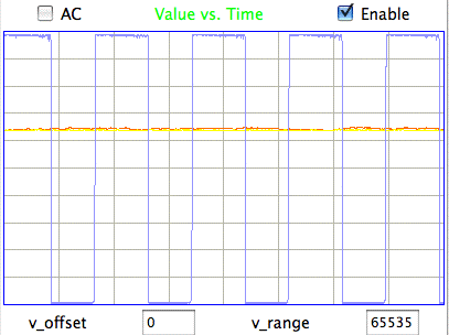
Figure: Square Wave Failure on 3.8. Taken from archive M1302907845. At the time of the recording, No8 had been implanted for seven weeks. The problem started after six weeks implanted.
We inspected 4.1 and 4.2 from CHB today, and found no sign of damage to the encapsulation or the lead bases. The No2 antenna had come out of its tube, but it did not look corroded. The No1 antenna tube was unsealed at the tip, and there was corrosion on the length of the antenna, but none at the base, where the epoxy bead stopped further penetration.
[25-APR-11] Delayed failures can be caused by broken capacitors and resistors. Both can fracture during surface-mount assembly or when the board is flexed during subsequent handling. According to reports like this one, modern assembly methods cause very few fractures, so that most fractures these days are flex fractures.
We observed fractures in three resistors while testing 80 A3019 assemblies. On three other boards, C4 was incorrectly soldered. When we replaced C4, the replacement worked. Today we replaced C4 on a board and tested the original part afterwards. Its capacitance was 3.7 μF. This capacitor is hard to reach because it is tucked between three larger components.
The circuit board is only 0.8 mm thick, instead of the usual 1.6 mm. It is four times more prone to flexing than a standard board. The A3019 assembly is made in panels of ten, out of which the individual circuits must be broken along score lines. Further flexing could occur when we calibrate and encapsulate the sensors.
We have seen ceramic capacitor fractures before. A fracture might cause no problem for months. When a problem first appears, it is intermittent and temperature-dependent. Later, it becomes permanent. In our experience, a fractures result in an open circuit, although we read that capacitors can fracture and cause a short circuit. It could be that the oscillation we see above is due to a fracture in gain resistor R11. It could be that a failure of decoupling capacitor C2 will allow 18 Hz noise onto the amplifier power supply.
We have an A3019P that we dedicated to circuit tests. We left the inputs open circuit with no leads. We removed and replaced various components. We measured the input noise as we went along.
| Change | Symptom |
|---|
| None | 0-160 Hz noise 13 μV, 100-250 Hz noise 11 μV, 18 Hz none |
| Remove C1 | Stuck on or off |
| Remove C2 | No effect |
| Remove C3 | No effect |
| R2 → 0Ω | 0-160 Hz noise 14 μV, 100-250 Hz noise 16 μV |
| Remove C2 and C3 | No effect |
| Remove C2 and C3 and R2→0Ω | 0-160 Hz noise 1000 μV |
| Remove C4 | no transmission |
| Remove C6 | no transmission |
| Remove C9 | gain on X drops from 100 to 5 |
| Remove R11 | No input voltage, X stuck at 65535
With mains hum, X is 60-Hz full-scale square wave |
Table: Symptoms of Open-Circuit Capacitor Failure.
Several of the capacitors are redundant. Resistor R2 gives us a slight reduction in high-frequency noise from the digital circuits. We see no intrusion of 18 Hz noise when we remove C2 and we see no 1-Hz self-induced oscillations when we remove R11.
Another source of gradual failure is corrosion and by residual solder flux. We use water-soluble acid flux to attach the antenna and leads. We take care to soak the circuits in hot water, clean them with a brush, and rinse them in hot running water. We always inspect for flux residue. We note that R11 is next to the X terminals, and most certainly gets covered in acid flux while we solder the leads in place.
[26-APR-11] While making transmitters yesterday, we discovered that blowing air on our transmitters and letting them sit for an hour does not remove all moisture from beneath the components on the circuit. Perhaps it is trapped moisture that is causing our gradual failures. Trapped moisture eventually corrodes solder and copper joints, creating ionic compounds that conduct electricity. We changed our encapsulation procedure to include a one-hour bake at 100°C to ensure that all moisture is evaporated before we encapsulate.
We receive recordings from Joost at ION from a set of 12 transmitters we shipped them at the beginning of January. Here is what we deduce from the recordings.
| Transmitter | Status |
|---|
| 2.8, 2.10, 2.11 | batteries exhausted |
| 2.9 | broken: 1 Hz full-scale square wave |
| 2.12 | was okay, but binned with animal corps |
| 2.1, 2.2, 2.3, 2.4, 2.7, 2.13 | okay, should run >2 weeks |
| 2.6 | battery exhausted or broken switch, don't know which |
Table: Status of Transmitters Twenty Weeks After Shipping. The transmitter name is a set number and its channel number.
We damaged transmitter 5.4 today while clipping off the programming extension. We were holding it between thumb and finger. Later, we found that the transmitter would not turn off. We noted that U2, a tiny 5-ball BGA, was not level on its footprint, even though the balls had flowed. We removed U2 and found that the pad for U2-3 had snapped off. We loaded a new part and the transmitter works.
There were three A3019P circuits in our "failed circuits" bag. One of them would not turn on and off. We replaced U2. Now it works fine.
[29-APR-11] Today we turn on the noisy transmitter 4.1 we describe above, and find that its input is now showing full-scale oscillations at around 1 Hz, just like UCL's 2.9 and 3.8. The 4.1 transmitter X leads are soldered together.
Figure: Start of Square-Wave Failure. This transmitter, 4.1, previously showed 18-Hz noise (see here).
Note: On 04-MAY-11 we discovered that transmitter 4.1's X leads were both broken at the base, and we are able to make contact by flexing the leads.
[02-MAY-11] Transmitter 4.1 was off on Monday morning. We assume it turned off of its own accord over the weekend. We turned it on. The square wave was gone. The input noise with leads shorted together was only 8 μV, of which 4 μV was 18 Hz. With leads open, we see mains hum of only 40 μV and the sensor cannot detect heartbeat. We conclude that the gain of the amplifiers has dropped by a factor of ten. The transmitter may have turned off because its battery was drained.
[03-MAY-11] Transmitter 4.1's battery voltage appears to be down to 2.2 V today. We estimate battery voltage with 1.8×a÷65535, where a is the average value of X. We turn 4.1 off for four hours. When we turn it back on, its voltage appears to be 2.7 V again. We leave it running. The X input is much as it was yesterday. We note that 4.1 was encapsulated on 01-FEB-11 and shipped a few days later. That's thirteen weeks ago, which is not enough for the battery to run down in a functioning transmitter, even if it were left on all the time.
[04-MAY-11] Transmitters 5.1-5.13 and 4.14 are encapsulated. These are destined for Rob Wykes at UCL. They pass the harmony and heartbeat tests. We place them in water, with their leads mixed up and separated. We look for noise from the Hall Effect Switch, which will show up as a peak between 15 and 20 Hz.
Figure: Hall Effect Switching Noise on Newly-Encapsulated Transmitters. The fourteen transmitters are totally immersed in water, and have been for no more than an hour. Signals recorded in M1304532983.
Transmitters 5.8, 5.9, and 5.13 show no sign of a peak at any frequency. The others show peaks between 15 Hz and 20 Hz of amplitude 3 μV to 8 μV. Total noise amplitude in 0-160 Hz varies from 4 μV to 28 μV rms. The following plot compares the full-spectrum noise of three transmitters.
Figure: Hall Effect Switching Noise from Three Selected Transmitters, 5.1, 5.9, and 5.10. Signals recorded in M1304532983. Noise in 0-160 Hz is 11 μV, 10 μV, and 27 μV rms respectively. The noisiest transmitters are 5.3, 5.5, and 5.10.
The 5.10 transmitter has an 8-μV peak at 18.625 Hz. We see noise throughout the pass-band of the A3019D's 160-Hz low-pass filter. Above 160 Hz, the noise attenuates, but not as sharply as it would if it were subject to the full attenuation of the three-pole 160-Hz low-pass filter.
[04-MAY-11] We took a closer look at 4.1's leads and antenna. It turns out that both the X springs are broken near the base, as you can see in this photograph. The failure of this transmitter during implantation was an absence of EEG signal. In the absence of EEG, we noticed the 18 Hz noise. But the noise itself was not the cause of failure.
Battery voltage appears to be 2.0 V. If we press on the leads at the base, we can get one or both of them to make contact again, and at that point we can pick up mains hum, but sensitivity is still poor. We still see 4 μV of 18 Hz noise. We turn off and heat the transmitter for a minute, turn on again, and battery voltage rises to 2.6 V.
[05-MAY-11] We go back and look at M1294435389, recorded on 07-JAN-11, which shows the signal from 3.2, 3.6, 3.7, 3.8, 3.10, and 3.12, which we sent to Rob at UCL soon after. At time 60 s we see the input noise when the transmitters are immersed in water. We see switching noise on transmitters 3.7 (16.25 Hz, 2.5 μV), 3.8 (17.0 Hz, 2.5 μV), and 3.12 (16.125 Hz, 1.7 μV). Transmitter 3.8 subsequently failed with 1-Hz oscillations.
We check the 14 transmitters immersed in water and obtain this plot of switching noise, which is much the same as yesterday's. We try transmitters 5.14 and 6.1, which are A3019As freshly encapsulated. Number 5.14 shows a 3-μV peak at 15.5 Hz, while 6.1 shows a 1.5-μV peak at 18.25 Hz, as you can see here. They pass the heartbeat and harmony tests. With inputs shorted together or in water, noise is around 12 μV from both.
We have seven functioning unencapsulated transmitters with programming extension, no antenna, and no leads. We power each one in turn with a battery on a connector, check the Hall Effect Switch is working, and look for switching noise. We see none. We are certain the switching noise is less than 1 μV in all cases. We select transmitter 0.5. We attach antenna and leads, clean, dry, and connect a battery to one of them. Still no switching noise. We solder a 1000 mA-hr batter onto the transmitter (we want to make our first A3019E). No switching noise. We put electrodes in water, no noise. We remove transmitter 4.5 from water and short its inputs. We see the same 4-μV switching noise as when it is in water.
[06-MAY-11] switching noise appears to have subsided substantially for the fourteen transmitters in water, as you can see here. The frequency of the 5.10 peak has moved from 18.625 Hz to 18.5 Hz. We compare the input noise to baseline EEG above.
We encapsulate our 0.5 transmitter. While the epoxy is still wet, we look for switching noise and find it. See here. We see amplitude 1.2 μV at 15.625 Hz. We put the transmitter in the oven to cure the epoxy. When we take it out, we cannot see the 15.625 Hz noise. We see no noise peak between 10 Hz and 25 Hz.
We take the fourteen transmitters out of their beaker of clean water, one after the other, and touch each with a magnet. After we touch the fourteenth, they are all turned off. We reverse the process, and all fourteen are on at the end. We immerse them all in warm 1% saltwater. We look at noise in 15-20 Hz. The noise peaks have vanished. Three hours later, the water has cooled to room temperature, and the peaks have returned.
[08-MAY-11] We placed the fourteen transmitters in pure water at 40°C. We lowered the temperature in stages with the help of water at 14°C from a drinking fountain. At each water temperature, we wait for one minute and measure the amplitude of the 18.5-Hz peak generated by 5.10's Hall Effect Switch. We obtain the following graph of noise versus temperature.
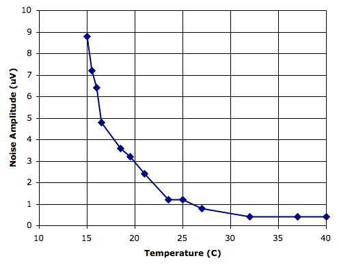
Figure: Switching Noise Amplitude on the Input of 5.10 versus Temperature. We determine the amplitude by looking at the peak in the 15-20 Hz band for an eight-second interval. The graph gives the impression that the switching noise is going to keep going up sharply. But this turns out not to be the case.
We cooled our epoxy-encapsulated 0.5 transmitter with freezer spray and saw its switching noise rises from 1.2 μV to a 2.0 μV. We cooled an unencapsulated transmitter and saw no switching noise.
[09-MAY-11] We use the HES Acquire script with the Acquisifier to record temperature and switching noise amplitude in the 15-20 Hz band.
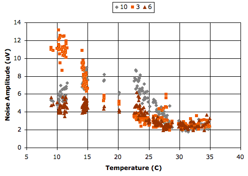
Figure: Switching Noise Amplitude versus Temperature. We present the amplitude for three transmitters. The amplitude is the rms value of the signal after filtering a four-second interval to 15-20 Hz.
Switching noise in 5.10 decreases below 15°C. The 15-20 Hz amplitude drops below 4 μV for all transmitters at 30°C.
[09-MAY-11] We receive a detailed report from Rob at ION, describing the state of each of the 14 transmitters 3.1 to 3.14 we sent to him in January. One transmitter failed six weeks into its first implant, generating 1 Hz oscillations. Another failed six weeks into its second implant, generating noise. Another failed three weeks into its second implant, with intermittent connection to EEG. The others are working fine. One is a week into its third implant. None have exhausted their batteries.
[11-MAY-11] We complete our first A3019E today. We used rejected circuit 0.5, whose current consumption is 120 μA (30 μA higher than we allow). We set it running to see how long it will last. In theory, it should run continuously for a year.
[27-MAY-11] Three more implanted transmitters have failed at CHB. The 4.5 transmitter, which ran well for two weeks in its first implant, would not turn on after explanting. The 4.7 transmitter is not picking up EEG. The 4.6 transmitter suddenly started generating its own noise 17 hours after implantation, at time 3098 s in archive M1306224760. We see large transients for ten seconds, and then the signal shown below.
Figure: Noise on 4.6 and No Signal on 4.7.
In a letter to CHB, we propose that their antennas are penetrating the antenna tubes after being stretched to double their length during implantation and explantation. We place an old A3019A in water with a bare antenna. Its electrode leads are cut off at the base. We see noise of 1.8 mV rms, spread throughout the 160-Hz bandwidth as you can see here. When we place the antenna in water, but the leads out of the water, or visa versa, there is no noise. If we connect the analog leads with the water through our finger, while immersing the antenna in water, the noise appears. But at the same time, other transmitters immersed in the same water do not pick up the noise. The transmitter's own inputs are not differential with respect to the antenna noise, while those of other transmitters are differential.
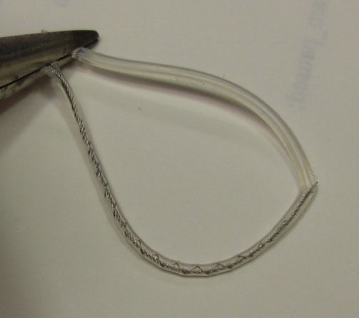
Figure: Antenna Loop After Stretching to Double Length. For closeup of breach, see here.
The above photograph shows how an antenna will penetrate its insulating tube after being stretched by a 500-g force. In an encapsulated transmitter, this force is carried by the base of the electrode leads. The silicone around the bases is thick and strong, but the springs themselves can stretch within the silicone, and so become weakened or break. We suspect this is how the leads of transmitter 4.1 were broken.
We will avoid damage like this in the future by coating the antenna directly with silicone.
[22-JUN-11] We receive from ION transmitters 2.6, 2.7, and 2.9. Transmitter 2.9 turns on and picks up mains hum with the correct gain. When immersed in water produces a white noise spectrum with a 2-μV peak at 20 Hz for its switching noise. We see no damage to the encapsulation or leads. Transmitters 2.6 and 2.7 will not turn on.
[15-JUL-11] After a few weeks in water, 2.9 picks up heartbeat but not mains hum. We see water beneath the silicone at the base of the leads. By squeezing in the right place, we see water emerging from between the leads and the antenna tip, where they are bound together by heat shrink. This transmitter is of an early construction, in which the binding is close to the transmitter body, creating a rigid lump. We moved the binding away from the transmitter later, and now we see that this is a good thing for two reasons. First, it relieves stress, and second it prevents the gap between the wire bundle from extending into the encapsulation. We play around with 2.9 some more. It is hard to turn on and off, and we observe the 1-Hz square wave that originally appeared during implantation. We put the transmitter in the oven and leave it to dry out.
[01-AUG-11] Our A3019E has failed. There was a problem with the circuit to start with, which caused its excessive current consumption.
2012
[07-FEB-12] We have seven new A3019Ds in water. On of them, No2, gives us a square wave when its leads are open circuit. When we connect a sine wave with 50-Ω source impedance, No2 gives the correct frequency response. When we connect a sine wave through two 10-MΩ resistors its gain from 2-40 Hz is 3 dB too high. We perform the same measurement for No1 and No4 and obtain the correct gain. We connect both No1 and No4 together and get the correct gain for two 10-MΩ input impedances applied in parallel to a 20-MΩ source impedance. When we connect No1 and No2 together, however, both transmitters record the same signal, but this signal is greater than it should be. We conclude that No2 is applying to its own input leads a signal with source impedance several Megaohm. This signal causes a square wave if the leads are open circuit, but adds to the input if the input is connected through a high impedance. Thus the signal responds to and is a function of the input frequency. In the case of transmitter 4.1 (see 04-MAY-11), when one of the leads was broken, the oscillation would begin.
We were eager to investigate further, but No2 stopped producing the square wave and stopped exhibiting its gain error. We recorded the gain of three transmitters here. Two other transmitters, No3 and No5, which exhibited the gain error stopped doing so during our experiments. So we must wait until we encounter another such transmitter and see if there is some kind of feedback from the antenna's 915-MHz transmission and the input leads.
[27-MAR-12] Out of a batch of 11 transmitters, 8 work perfectly after four days running in water, 2 have gain half what they should when supplied through 10 MΩ (transmitters 13.1 and 13.2), and 1 produces a square wave (transmitter 13.10). We remove the screws from 13.10, heat it with our heat gun, and restore the screws. At each stage the square wave persists. Symptoms are as described above in 07-FEB-12 entry.
Figure: Persistent Square Wave of 13.10.
We turned off all three faulty transmitters and put them in the oven at 60°C and went home.
[28-MAR-12] Took the three faulty transmitters out of the oven. All of them now perform perfectly. Their frequency response is within 1 dB of nominal from 1 Hz to 500 Hz. We suspect that a chemical reaction is going on within the transmitter, on the surface of the printed circuit board, causing conduction between pins, vias, and pads. There may be acid flux trapped under some of the components. It may be that the epoxy is inadequately mixed and reacts with the flux. We observed the square waves before we introduced nail polish as our encapsulation touch-up around the rim of the battery, so we doubt the reaction has anything to do with the acetone-based nail polish.
We note the battery voltage of all three restored transmitters started at 3.3 V and within ten minutes dropped to 3.1 V. We leave them running in water to see what happens. We expect battery voltage to drop to 2.7 V within 24 hours. We put the eight transmitters that passed the original frequency test in the oven at 60°C.
[29-MAR-12] After running for a day, 13.1 and 13.10 are still fine, but 13.2 is once again showing the previous symptom of 13.1 and 13.2: its gain is half what it should be. The remaining eight transmitters are still working perfectly after a night in the oven. This suggests that the problem with 13.1 and 13.2 will persist. We resolve to tin leads with acid flux and wash them before we solder them to the circuits. Thus we will ensure there will be no acid flux residue on the boards, only our no-clean aqueous flux, which we will wash off thoroughly in hot water.
For the past month we have had in our posession three transmitters returned from CHB. Each had been through at least two implants, and all had their leads and screws replaced, cut, and spliced in some way. They are No4, No9, and No11. All had perfect input response on arrival. All have five coats of silicone. The coating on No4 and No9 is wrinkled and appears to have come detached in most places. We leave them in water for a week. No4 is unreliable turning on and off. We let them sit in air for three weeks. Today we removed the silicone from No4 and No9. There is no sign of water damage beneath, but adhesion with the nail polish surface was poor. No11, without nail polish around the edges, appears to have good adhesion between the silicone and epoxy, but poor adhesion around the battery edge. We measure input reponse and find it perfect for all three. Battery voltage for No4, No9, and No11 is 2.65 V, 2.72 V, and 2.67 V respectively.
[05-APR-12] We complete transmitters 13.12, 13.13, 13.14, 14.1, 14.2, and 14.3. All have frequency response within ±1 dB of nominal. We measure switching noise at 17°C and observe 2.4 μV at 16.5 Hz on 13.13, 1.6 μV at 15.0 Hz on 13.14, 3.2 μV at 18.5 Hz on 14.1, 1.6 μV at 18.3 Hz on 14.3, and less than 0.8 μV on the other two. Transmitters 13.1 and 13.10 are still working perfectly, but 13.2 still has half the nominal gain.
[09-APR-12] The six new transmitters are still working perfectly. We see no sign of reduced gain or square waves. These were made without using acid flux on the circuit boards. Meanwhile, 13.2 now has the correct gain, and matches 13.1. Transmitter 13.10 is also workind perfectly, so we include it in a shipment of 14 transmitters to ION on Job 1127.
[13-APR-12] Transmitter 13.2 has half the nominal gain once more, and 13.1 now has half normal gain as well.
[18-MAY-12] Transmitters 13.2 and 13.1 have the correct gain and function perfectly.
[28-JUN-12] We made 3 A3019F transmitters (2048 SPS). Use red dye for X+ lead 150-mm long. Use blue dye for X− lead 150-mm long. Both leads have bare wire ends. They work fine a week after encapsulation. We made 8 A3019D transmitters. Use orange dye for X+ lead 150-mm long. Use green dye for X− lead 150-mm long. Both leads have bare wire ends. We did not apply acid flux directly to the boards. We did not attach screws. We baked to remove moisture. The epoxy we were uncertain about: some of it may not have mixed in equal parts because of an obstruction in the outlet of the cartridge. After two hours in the oven and a day at lab temperature, the epoxy surface was still sticky. We encapsulated with silicone. A week after encapsulation, 4 out of 8 were generating square waves when their leads were open-circuit. The symptoms are the same as those we describe in our 07-FEB-12 entry. We placed the transmitters in an oven at 75°C for 2 hours. All transmitters were working perfectly after that. Left running in water with one lead in air. A day later, today, No8 shows square wave of 3 Hz.
[02-JUL-12] No8 still showing square wave, others are fine. Turn all of them off and put them in the oven at 60°C.
[03-JUL-12] After 30-hour bake at 60°C we remove all eight transmitters, turn them on, and put them in water with X+ in air. All eight look good, except No8 has slightly lower battery voltage.
[05-JUL-12] All eight transmitters look good with matching battery voltages. No sign of switching noise today at 20°C, even though we saw switching noise in three or four of them before the prolonged bake.
[17-JUL-12] Prepared 11 A3019As. Use red dye for X+ lead 50-mm long. Use blue dye for X− lead 50-mm long. Both leads have M0.5 screws. All have good frequency response. No2 has short-circuit noise 60 counts rms instead of the expected 30 counts. The others have noise between 25 and 40 counts rms. We allowed them to run for 4 hours in water, checked their frequency response, and now leave them off to soak in water.
[31-OCT-12] Prepared 10 A3019As. Use red dye for X+ lead 45-mm long. Use blue dye for X− lead 45-mm long. Both leads have M0.5 screws. Used fresh epoxy cartridge. Baked them after epoxy encapsulation for 24 hours. Serial numbers are 15.12-15.14 and 16.1-16.7. We add to these 15.11 from July and test. No sign of square wave in any. Switching noise in cold water that quiets down in warm water. Leave to soak. Photograph here. At 19°C we see switching noise of 10 μV in 16.6 and lower amplitude in four other transmitters.
[01-NOV-12] Checked on our 11 A3019As at 19°C in water. The figure below shows the spectrum of the Hall Effect Switching noise for all eleven.

Figure: Spectrum Hall Effect Switching Noise. Shown for eleven A3019As in water at 19°C.
When we use the spectrum to calculate the root mean square amplitude of the signal within a low and a wide frequency band, we obtain the following results.
| Transmitter |
10-20 Hz 19°C
(μV rms) |
4-160 Hz 19°C
(μV rms) |
10-20 Hz 35°C
(μV rms) |
4-160 Hz 35°C
(μV rms) |
| 15.11 | 6.3 | 13.9 | 2.8 | 7.3 |
| 15.12 | 2.5 | 8.3 | 2.1 | 7.4 |
| 15.13 | 7.5 | 18.3 | 2.9 | 8.2 |
| 15.14 | 6.3 | 15.0 | 2.2 | 7.8 |
| 16.1 | 2.4 | 8.5 | 2.4 | 6.7 |
| 16.2 | 5.5 | 13.7 | 5.2 | 15.4 |
| 16.3 | 3.5 | 10.2 | 2.0 | 7.7 |
| 16.4 | 3.1 | 9.3 | 1.9 | 7.3 |
| 16.5 | 3.2 | 9.2 | 2.7 | 10.5 |
| 16.6 | 10.1 | 26.3 | 2.9 | 6.9 |
| 16.7 | 3.4 | 9.0 | 3.3 | 7.1 |
Table: Signal Amplitude in Water Bath.
Transmitter 15.13 and 16.6 are particularly noisy at 19°C. They each have a large switching noise peak and a high noise amplitude across the spectrum. Here we see them compared to a quieter channel.
Figure: Signal and Spectrum from Three Transmitters in Water at 19°C. We see the traces for transmitters 16.4, 16.6, and 15.13.
The table also shows the noise we observe when we place the transmitters in water at 35°C which we expect is closer to the temperature at which they will operate when implanted in live animals. The switching noise diminishes greatly, and we obtain the following signal and spectrum for the same three transmitters.
Figure: Signal and Spectrum from Three Transmitters in Water at 35°C. We see the traces for transmitters 16.4, 16.6, and 15.13.
We do not understand why the switching noise reduces with temperature, nor why it varies so greatly from one transmitter to the next, but we are confident that these transmitters will perform well when implanted.
[07-NOV-12] We receive from Sukhvir Wright at Oxford University the following screen shot of the trace from transmitter 15.8.
Figure: Recording from 15.8, One-Second Interval. Transmitter has been freshly implanted.
This signal looks like noise of amplitude 300 counts rms. Louise Upton reports that this transmitter does not exhibit noise when it is dropped in water. Sukhvir reports that the noise amplitude reduced by half a day after implantation.
[16-NOV-12] We receive from Sukhvir a recording from 15.8 after a day implanted. The following figure shows the signal and its spectrum.
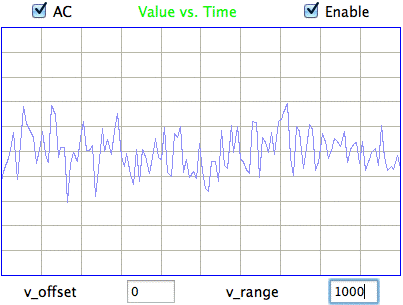
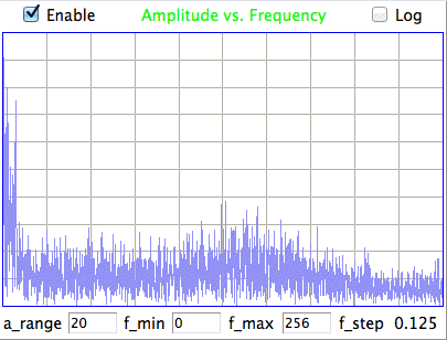
Figure: Noise on 15.8 a Day After Implantation. Left: voltage versus time over 250 ms interval. Right: Amplitude versus frequency for 8-second interval.
[16-NOV-12] We complete 10 A3019D transmitters for ION. We took care over epoxy mixing and baked to cure over the weekend at 60°C. No sign of the square wave problem. Nine perform perfectly. But 16.11, is noisy, as shown below.
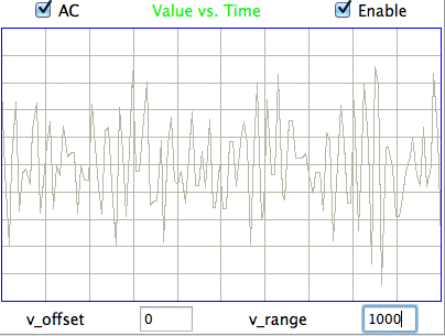
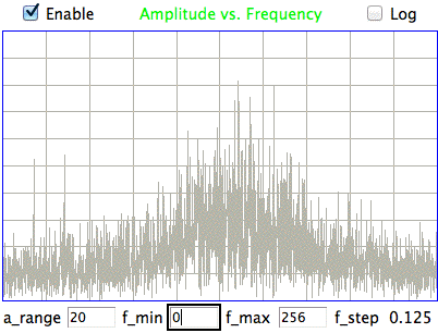
Figure: Noise on 16.11 Immersed in Water. Left: voltage versus time over 250 ms interval. Right: Amplitude versus frequency for 8-second interval.
When we connect 16.11 to 30-Hz, 30-mV p-p with 20-MΩ source impedance we expect to see a sinusoidal signal of amplitude roughly 8800 counts rms. But instead we see only 2000 counts rms. When we try to measure heartbeat with 16.11, we see only 60 Hz mains hum of amplitude 10 mV p-p or higher.
[17-DEC-12] We complete 13 A3019D transmitter for ION. When we loaded the battery, we inspected each transmitter to make sure that the 0-V terminal did not come close to touching pin U7-2, which is the TUNE input to the RF oscillator. We baked over the weekend at 60°C to cure epoxy. No sign of square wave problem or noise problem. Frequency response is close to nominal except in 17.8, where we do not see the 3-dB rise in gain before the cut-off frequency. Nevertheless, 17.8 is still within 3-dB of nominal for all frequencies, so we will ship it.
[17-DEC-12] We take out 16.11. The peak in its transmission spectrum is at 915 MHz, and the signal is strong. But when we place its antenna next to our receive antenna, we detect only 280 SPS of the 512 SPS transmitted. In water, the input noise is 170 counts. Reception is accompanied by an average of 50 or so bad messages per second. When we turn off 16.11, the bad message rate drops to 20 per second. [This turns out to be a problem with the Data Receiver, see below.]
[28-DEC-12] We solder leads and antennas to 14 A3019A transmitters. We obtain poor reception from all of them and conclude we have a problem with the Data Receiver. This turns out to be the case. We repair the Data Receiver and obtain perfect reception from all fourteen transmitters, including 16.11. We now observe no gain at all on the X+ input of 16.11, nor does the 60-Hz mains hum disappear when we connect its inputs together. We conclude that X+ is not connected to its lead. Within an FE2B faraday enclosure, we see 200 counts of noise.
2013
[08-JAN-13] Transmitter 16.11 will not turn on.
[08-JAN-13] We have 14 of A3019A in water, freshly encapsulated. We forgot to put the labels on until after the fifth coat of silicone. So we put on the labels and did a applied one more coat of silicone, from just abouve the label to the bottom. This worked out well, and served to smooth the cut-off at the drip on the bottom corner.
We record from them for one minute and obtain archive M1357667472. We obtain the following plot of switching noise.
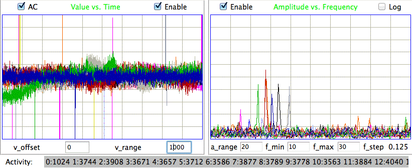
Figure: Hall Effect Switching Noise in Fourteen A3019As. All transmitters in water at temperature 21°C.
Reception for this same eight-second interval is as follows. We obtained the reception details using the Versbose option in the Neuroarchiver.
Using 54190 messages, including 1024 clocks.
Channel  1,  8.6% loss, 4096 reconstructed, 0 bad.
Channel  2,  4.6% loss, 4096 reconstructed, 1 bad.
Channel  3, 10.4% loss, 4096 reconstructed, 0 bad.
Channel  4, 10.8% loss, 4096 reconstructed, 1 bad.
Channel  5,  9.4% loss, 4096 reconstructed, 1 bad.
Channel  6, 12.5% loss, 4096 reconstructed, 0 bad.
Channel  7,  5.4% loss, 4096 reconstructed, 0 bad.
Channel  8,  7.5% loss, 4096 reconstructed, 1 bad.
Channel  9,  7.8% loss, 4096 reconstructed, 1 bad.
Channel 10, 13.0% loss, 4096 reconstructed, 0 bad.
Channel 11,  5.2% loss, 4096 reconstructed, 0 bad.
Channel 12,  1.4% loss, 4096 reconstructed, 0 bad.
Channel 13,  4.3% loss, 4096 reconstructed, 0 bad.
Channel 14,  1.4% loss, 4096 reconstructed, 0 bad.
The values above are typical. We rarely see more than 16% loss in any one transmitter, and usually around 8%. We check frequency response of all 14 transmitters and find them to be within 2 dB of nominal from 1 Hz to 250 Hz.
[22-JAN-13] We measure the volume of one of our new A3019As with four coats of silicone and find it to be roughly 1.3 ml without the antenna and leads. This is 0.3 ml higher than the 1.0 ml volume we measured previously with three coats of silicone.
[13-FEB-13] We receive eight transmitters back from Dennis at ION. Failures by transmitter serial number. Where Dennis's notes don't give the year, we have assumed 2012.
9.14, encapsulated 19-SEP-11, large 2-Hz oscillations on 01-OCT-12, switching off by itself. Dead on return 12-FEB-13. May have been left turned on for a couple of months while waiting to be implanted.
10.5, encapsulated 02-OCT-11, large 37-Hz oscillations in animal 01-OCT-12. Ran perfectly in water 11-FEB-13 to 13-FEB-13. Shows correct noise in water, correct mains hum in air, correct amplitude of human heartbeat. Battery voltage 2.7 V. Can't explain original oscillations.
10.6, encapsulated 02-OCT-11, did not switch on first use 26-OCT-12. Dead on arrival 11-FEB-13. May have been left turned on for a couple of months while waiting to be implanted.
10.7, encapsulated 02-OCT-11, did not switch on first use 29-SEP-12. Dead on arrival 11-FEB-13. May have been left turned on for a couple of months while waiting to be implanted.
11.2, encapsulated 11-JAN-12, large 75-Hz oscilations on first use 26-SEP-12. Running on arrival 11-FEB-13, measures mains hum in air. Battery voltage 2.2 V. Switched it off with magnet and it won't turn on again. Can't explain original oscillations.
11.8, encapsulated 11-DEC-11, did not switch on first use 26-SEP-12. May have been left turned on for a couple of months while waiting to be implanted.
14.8, encapsulated 22-Jun-2012, square waves on first use JAN-13. This transmitter showed square waves when first encapsulated, and not after a 30-hour bake at 60°C, as reported above in entries of June 2012. We shipped this transmitter to ION on 05-JUL-12. Ran perfectly in water 11-FEB-13 to 13-FEB-13. Shows correct noise in water, correct mains hum in air, correct amplitude of human heartbeat. Battery voltage 2.8 V. Can't explain original square waves.
14.14, encapsulated 22-JUN-2012, died on third implant 10-NOV-12 after eight days running. Dead on arrival 11-FEB-13. May have been left turned on for a couple of months while waiting to be implanted.
Five of them may have failed because they were left running while waiting to be implanted. Three of them showed oscillations while implanted. Of these, one was running when it arrived here and had no battery left, and the other two have plenty of battery left and are working perfectly. We have no explanation for the oscillations while implanted.
[20-FEB-13] Measure gain versus frequency for 10.5 and 14.8. The gain of 14.8 is within 2 dB of nominal. But the gain of 10.5 starts to rise at 50 Hz, reaching a peak of 8 dB above nominal at 95 Hz and returning to nominal at 160 Hz.
[22-FEB-13] Dennis reports that transmitter 14.11 is showing large oscillations. This transmitter, along with 14.8, were members of a batch of eight transmitters half of which had the square-wave problem.
[25-FEB-13] Gain of 10.5 no longer shows rise at 95 Hz. Instead, the gain is roughly 2 dB too low all the way through the pass-band of the low-pass filter. Gain of 14.8 is normal. We test 14 new transmitters, 19.3 to 20.2 after three days in water. All perform perfectly except 19.4, which has high gain from 2-40 Hz as we observed on 07-FEB-12. This problem we associate with the self-oscillation of the transmitter. We bake 19.4 for three hours at 60°C and its frequency response is now normal. We leave 10.5 in the oven to bake at 60°C.
[01-MAR-13] Transmitter 10.5 response unchanged by four-day bake at 60°C. Still roughly 2 dB too low all the way through.
[06-MAR-13] Transmitters 10.5 and 14.8 have been operating normally and continuously for five days with their electrodes in open air. They pick up mains hum but do not generate square waves.
[07-MAR-13] Transmitter 10.5 is now oscillating. We record for 60 s to M1362667838. For the first 10 s, the X electrodes are connected. From 10 s to 20 s, they are disconnected in air. From 20 s to 60 s, the transmitter and its electrodes are in water. The following screen shot shows the oscillations during a one-second interval with the transmitter in water.
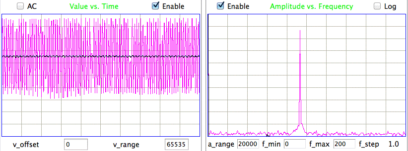
Figure: Oscillations of 10.5. The oscillation frequency is 95 Hz. The transmitter and its electrodes are in water.
The oscillation frequency is 95 Hz, which is the same frequency at which this transmitter displayed a +8 dB peak in gain on 20-FEB-13. Transmitter 14.8 is still running without problems.
[11-MAR-13] Transmitter 10.5 still oscillating with amplitude 20,000 counts rms at 95 Hz. Take it out of water, turn it off, and put it in the oven at 60°C. No 14.8 still running without problems.
[13-MAR-13] Transmitter 10.5 has been baking for 48 hours. We take it out and turn it on. It no longer oscillates. We measure its frequency response and find it to be roughly 2 dB below normal, but no sign of a peak in gain at 95 Hz. We leave it running. No 14.8 is still running. Its frequency response is normal.
[14-MAR-13] Transmitters 10.5 and 14.8 running fine, detecting mains hum.
[19-MAR-13] Transmitter 10.5 is once again generating its own oscillations. We measure their frequency and amplitude with the Neuroarchiver and obtain 91 Hz and 21,000 counts rms.
[25-MAR-13] Transmitter 10.5 has stopped oscillating and is running fine. We measure the frequency response. Instead of being 2 dB lower than nominal, it is 1 dB higher. There is no sign of a peak in gain at 90 Hz. Although we left the 10.5 in water, the water had evaporated over the past week, so only the bottom half of the transmitter body was immersed. We add water and immerse the transmitter fully, leaving it running. Transmitter 14.8 is running fine.
[27-MAR-13] Transmitter 10.5 is oscillating again, but now at 55 Hz. We remove it from the water to let it dry out.
[28-MAR-13] Transmitter 10.5 dried out and no longer oscillating, but detecting mains hum. No 14.8 normal in water.
[29-MAR-13] Transmitter 10.5 still dry and behaving well. No 14.8 normal in water.
[01-APR-13] Transmitter 10.5 still dry and behaving well, detecting mains hum. No 14.8 normal in water. We take transmitter 18.7 from the shelf. It detects heartbeat. Battery was loaded 31-DEC-12, so we have used 3 months at 5 μA, which is 11 mA-hr of the 48-mA hr battery life. Battery voltage is now 2.77 V.
[08-APR-13] Transmitter 10.5 still dry and behaving well. No 14.8 normal in water.
[17-APR-13] 10.5 still dry and behaving well, 14.8 in water and behaving well. We inspect 10.5 with a loupe all over, looking for breaks in the encapsulation, but find none. We see signs of corrosion around the antenna, and the space beyond the antenna in the silicone tube is filled with a white gas of fluid. We put 10.5 back in the water to see if it will go wrong again.
[18-APR-13] Transmitter 10.5 now oscillating at 55 Hz, after only 24 hours in water. We see water moving around beneath the silicone at the base of the antenna. We inspect again, but still cannot see a break in the encapsultion. We inspect 14.8 and see a layer of water between the battery and the silicone near the base of the antenna. We cannot find a breach in the silicone, although we see flaws immediately above the water. The antenna does not look corroded, but the insulation is thin in places.
[22-APR-13] Remove 10.5 and 14.8 from oven. So far as we can tell, there is no water beneath the silicone any more. But there is an air-filled cavity instead, or silicone we can move with our thumb. Both transmitters behave normally. We now suspect that water at the base of the antenna causes the oscillations.
[08-MAY-13] Transmitters 10.5 and 14.8 still dry and behaving well. They have been running continuously now since 20-FEB-13, or 11 weeks. Battery voltages are 2.66 V for 10.5 and 2.63 V for 14.8. We try out an A3019P with a lithium-ion battery. It works fine. The average value of X is 31342, for a battery voltage of 3.76 V.
[12-JUN-13] Transmitters 10.5 and 14.8 have exhausted their batteries. They will turn on briefly to show battery voltage around 2.1 V, then turn off.
[02-JUL-13] Some completed A3019A transmitters have been showing low gain when we connect them to our 30-mV, 20-MΩ sinusoidal voltage source. At first we assume this is the fault of the transmitters, but we find that after messing around for long enough, the transmitter will give us the correct gain and frequency response. We conduct tests that disprove all of the following hypothesis for why we might observe low gain occasionally.
- Bad contact in screw solder joint leads to attenuition of signal.
- When first turned on with leads in open air, transmitter can get into a state where it does not amplify properly.
- Water on the bottom of the test apparatus circuit board attenuates the applied signal.
- The conducting foam in the faraday enclosure is attenuating the signal when it happens to make contact with the clips.
- It matters which lead you connect to which clip.
One thing we changed in the test clip circuit board recently is we applied glue to the BNC plug so as to keep it still, and soldered the clips directly to the circuit. It may be that water is getting in under the glue and causing problems. We have water on our hands when we work with the voltage source because we are taking transmitters out of the bowl in which they have been soaking for two days.
[14-AUG-13] Of 14 A3019D transmitters that have spent three days soaking in water, four show a square wave and two show low gain, leaving eight that are correct. Inspection with a loop reveals holes in the antenna insulation of two of the square wave devices, numbers 24.10 and 24.11, but no other penetrations. The transmitters quickly get covered with lint and dust when we handle them. Our office is dirty.
Kirsten proposes that water is getting in by the path drawn below. Water can penetrate between the leads and the antenna. Because we clip the antenna from a longer section of insulated wire, the tip is not insulate prior to dipping the transmitter. The seal is therefore effective from the oustide, but it is not effective on the side where the antenna presses up against the leads. Thus water can reach the antenna tip by passing between the leads. Once at the tip, it wicks readily along the stranded antenna to the transmitter circuit board.
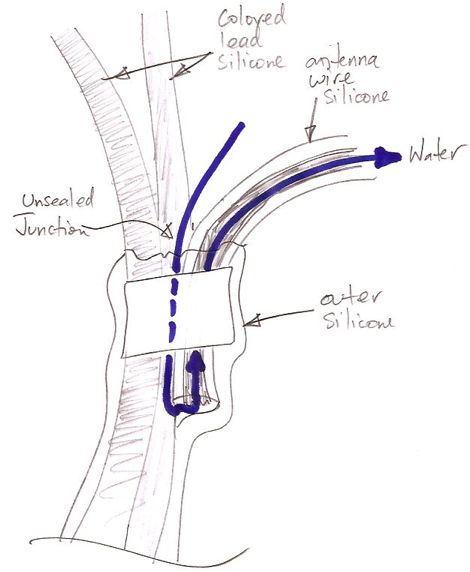
Figure: Possible Path for Water Penetration.
We baked all transmitters at 60°C for seven hours. All those that were faulty are now working perfectly. In the future, we will seal the antenna tip before we bind it to the leads. But for this batch, we inject silicone between the leads and antenna, cure, and repeat. We believe we have now sealed the space between the leads.
[15-AUG-13] Ship transmitters 24.7, 24.9, 24.12, 25.1, 25.2, 25.3. 25.4, and 25.5 to ION. We strip the insulation from the antenna of 24.14 and re-coat. Clean the office thouroughly.
[16-AUG-13] Place 24.6, 24.8, 24.10, 24.11, and 24.13 in water, turned on. We apply another coat to the antenna of 24.14.
[20-AUG-13] After three days in water, 24.6, 24.8, and 24.13 are still running perfectly. Transmitters 24.10 and 24.11 have square waves. These two are the ones with penetrations in their antennas, rather than the open-ended antenna. We bake them for a few hours and they recover. We leave 24.6, 24.8, and 24.13 in water.
[21-AUG-13] We coat 24.14 with silicone all over. Transmitters 24,6, 24.8, and 24.13 still running fine in water. Take 24.10 and 24.11 out of oven. They run fine. Leave them running in faraday enclosure in air. Later, place them in diluted red ink, stir them a few times and leave running.
[23-AUG13] Transmitters 24.6, 24.8, 24.13 still running well in water. We take them out of water and set them aside to ship to ION. Transmitters 24.10 and 24.11 are still running well in ink. No sign of ink penetrating along antenna. Transmitter 24.14 now fully repaired, place it in water.
[26-AUG-13] Transmitter 24.14 still running fine, leave in water. Transmitter 24.10 is running fine after five days in ink, but 24.11 shows a square wave. We examine the antenna for signs of ink penetrating, but see nothing. We put 24.11 in the oven and leave 24.10 and 24.14 in water. Leave an antenna wire in ink, un-coated end in the fluid.
[29-AUG-13] Transmitter 24.10 and 24.14 still running fine in water. Transmitter 24.11 fully recovered after 72-hour bake. We apply a coat of silicone to transmitter and antenna. The antenna in ink shows no coloration along the coated portion of the wire.
[05-SEP-13] Transmitter 24.11 has been sitting at room temperature for six days and runs fine. We place it in water, turned off. Transmitters 24.10 and 24.14 have been in water another six days and run fine when we turn them on. Clean them of slime that had grown around them, and place in fresh water, turned off.
[09-SEP-13] New batch of A3019As have been soaking in water for five days. Transmitter 25.8 has half the gain we expect, 25.14 has less than half, and 26.3 has the square wave problem, with high gain at 10 Hz. The others have normal gain or slightly higher than normal gain. Battery voltages appear to be 2.6 V. We place 25.8 and then 25.14 in parallel with 26.4 in our frequency response test stand. The amplitude of the signals on both transmitters is halved, as we expect from the combination of their 10-MΩ input impedances and our 20-MΩ source impedance. Thus the faulty transmitter shows lower gain than the working transmitter when connected to the same signal source. Thus the low gain we are observing today is a problem distinct from the square-wave problem, in which the transmitter creates a large signal and this signal is picked up by the second transmitter's leads, so that the the two in parallel read the same voltage. If the problem is with component values on the circuit, then it should persist through a bake in the oven. We put 25.8, 25.14, and 26.3 in the oven at 60°C. Transmitter 24.10 and 24.11 running fine. But 24.14 now showing high gain at 10 Hz, which we associate with the square wave problem. We leave in water.
After half an hour in the oven, 25.8, 25.14, and 26.3 show normal gain. We test them all after cooling to 0°C with freezer spray, and they are all normal. We place in water.
We left six transmitters soaking over-night in water, turned off. Transmitters 24.10, 24.11, 26.3 have nominal gain. Transmitter 24.14 has gain 3 dB too high at 20 Hz, and decending to nominal at 140 Hz. Transmitter 25.8 gain is around 2 dB below nominal. Transmitter 25.14 gain is 6 dB below nominal. We turn them all on and leave them soaking in hot water. We write to our customers describing the problem in an e-mail, Square Wave 1.
[12-SEP-13] We dry off the six transmitters we left in water. We place them on a table with their leads open-circuit. None of them produce the square wave. We wet our fingers and hold two X+ leads in our left hand and two X- leads in our right hand. We see positive bumps once per second that represent our heartbeat. Transmitters 24.10, 24.11, 24.14, and 26.3 all produce the same amplitude as one another when thus connected to our body. Transmitter 25.8 records hearbeat 4 dB smaller (2/3 amplitude) and 25.14 records 8 dB smaller (1/3 amplitude). We measure the resistance between our hands. It varies from 500 kΩ to 1.5 MΩ. When we place the transmitters in water, they all show noise of order 30 counts rms. Their X electrodes are separated by of order 1 cm. We measure the resistance between two points in water 1 cm apart: of order 1 MΩ.
We apply 10 mV with 50-Ω source impedance to all six transmitters and find their frequency response is within ±2 dB of nominal in all cases. We apply 30 mV with 20-MΩ source impedance. Transmitters 24.10, 24.11, 25.3, 25.8 have response within 2 dB of nominal. Transmitter 24.14 has gain at least 6 dB higher than nominal from 10 Hz to 40 Hz. It shows modulation of gain at around 4 Hz, and occasionally it oscillates. Transitter 25.14 shows modulation of gain from 10 Hz to 40 Hz, but on average its gain is within 2 dB of nominal. We leave all six transmitters running in water.
[17-SEP-13] We remove transmitters 24.10, 24.11, 24.14, 25.3, 25.8, and 25.14 from water. No square waves. We measure their frequency response. The graph below shows the frequency response of four of them. The frequency response of 25.3 and 25.8 is not plotted, but lay within ±1 dB of the response we show for 24.11 and 25.14.

Figure: Frequency Response of Four Encapsulated Transmitters. Letters A and D indicate A3019A and A3019D respectively. See text for history of problems with these transmitters.
Transmitter 24.14 still shows +6 dB gain at 20 Hz. Transmitter 24.10 show acceptable frequency response, but the bump at 130 Hz is missing. The remaining four have similar, correct response.
We take an un-encapsulated transmitter with 150-mm leads and attach a battery. Its frequency response is close to nominal. We take a foam applicator and dip it in water. We touch the bottom side of the transmitter circuit board on the X− pad, so as to deposit a film of water around X+. As soon as we apply the water, the X output starts to oscillate with a full-scale asymmetric wave of 4 Hz, as shown below.
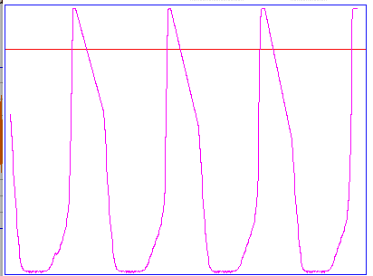
Figure: Square Wave Generated With Water Film. This is the wave we see thirty seconds after application of a water film between X+ and R11.
One minute after application, the oscillation is a 4-Hz square wave. At three minutes, the square wave is 5-Hz. At five minutes, the wave is 5 Hz, but does not reach full scale on the negative side. At six minutes, we have a 5 Hz wave that does not reach either top or bottom of the range. At eight minutes, the wave has amplitude 4000 counts rms. At nine minutes, the oscillation has stopped.
We can repeat this experiment as often as we like. We can stop the square wave at any time by blowing the circuit dry with nitrogen. Each time we perform the experiment, the waves we observe has a slightly different evolution. We cannot stop the square wave by holding one electrode in each hand, but the square wave stops immediately when we connect the electrodes together, or we place them both in the same beaker of water. This suggests the impedance of the film is of order a few megaohms.
[18-SEP-13] We take our six unreliable transmitters out of water and cool them with freezer spray until ice crystals form on the encapsulation over their amplifiers. We thought we might provoke condensation within the encapsulation, and so generate some square waves. But we see no change in the mains hum picked up by any transmitter. Put them back in clean, hot water.
[20-SEP-13] We assemble a batch of 14 A3019Ds. We load the battery using solder with a non-aqueous, no-clean flux core. We do not clean this flux off. We apply an acrylic conformal coating ("MG Chemicals 419C Acrylic Lacquer Conformal Coating") to the bottom surface of each circuit around the X input pads, and extending half-way across the circuit in every direction. This coating is suppose to bond to the solder mask and components, leaving no gap in which water could condense.
[23-SEP-13] We measure the frequency response of all 14 A3019Ds. All show the 3-dB Chebyshev frequency response with cut-off at 160 Hz. The amplitude at 130 Hz, at the bump before the cut-off, ranges from 8100-9500 counts rms, which is 8800±700, for a variation of ±0.6 dB.
[30-SEP-13] We left 14 of A3019D in water over the weekend. All had acrylic coating on R9, R10, R11, C8, and C9. None show a square wave when open-circuit. Of the fourteen, twelve show perfect frequency response and gain with 20-MΩ signal source. Transmitter 26.13 had gain −6 dB with 20-MΩ source and with 50-Ω source. Transmitter 26.11 had gain −3 dB with 20-MΩ source. We forgot to test 26.11 with a 50-Ω source. We bake these for 30 minutes at 60°C and now their gain is normal with 20-MΩ source.
These fourteen transmitters show no sign of increased gain at 1-40 Hz, the signature of the square wave problem. Their gain is not dependent upon source resistance. The low gain could be moisture around uncoated component C10, or between uncoated pins U8-6 and U8-7 (see component placement). We put 26.11 and 26.13 and in water.
Transmitters 24.10, 24.11, 24.14, 25.3, 25.8, and 25.14 have been turned off and sitting in water. We measure their response with a 20-Ω source. Transmitter 24.10 shows the same low gain without a bump that we measured on 17-SEP-13. This behavior is consistent with moisture around the second stage of the amplifier. Transmitters 24.11, 24.14, 25.14 are all fine. Transmitter 25.8 has −3 dB with 20 MΩ source and normal gain with 50-Ω source, suggesting water film around R9. Transmitter 26.3 still shows high gain from 1-40 Hz, and generates a square wave on its own at 5 Hz for ten seconds or so when provoked.
We note that 24.14 showed high gain at 20 Hz on 17-SEP-13, but is now normal. Transmitter 25.8 showed normal gain on 17-SEP-13, but now gives low gain. Transmitter 26.3 showed normal gain on 17-SEP-13, but now gives high gain at 5 Hz. Transmitter 24.10 shows the same low gain at 130 Hz that it did on 17-SEP-13. Transmitters 24.11 and 25.14 still show normal gain.
We add 24.11 to our 12 good transmitters to make a batch of 13, and resolve to ship to ION.
[16-OCT-13] We prepare a batch of 14 A3019A transmitters. We load the battery. We use solder with a non-aqueous, no-clean flux core. We do not clean this flux off. We apply acrylic conformal coating to the entire amplifier circuit. We encapsulate in epoxy and silicone, check their frequency response, turn them off, and leave them to soak in water. Today we took them out after five days in water and checked their frequency response again. All of them behave well. There are none with the low gain problem or the square wave problem. All show normal switching noise. If the acrylic coating did not affect these problems, and no other factors in the assembly have been changed, the chances of seeing no occurances in fourteen transmitter of either problem is around 5%.
[21-OCT-13] We have back from ION six transmitters that developed square waves while implanted. They have several weeks out of water. No14.9 "naturalistic TTX-resistant HF activity, don't reuse." Transmits well, no square wave, connecting leads eliminates mains hum. No14.11 "HF max-amplitude activity right after switch-on inside and outside rat with connected and disconnected leads." Transmits well, no square wave, connecting leads does not eliminate mains hum, picks up mains hum with X+ but not X−. No14.13 "high-amplitued oscilations developed two weeks after implantation". Transmits well, no square wave, connecting leads together eliminates mains hum. No22.3 "first or second implantation, high amplitude oscillations after 5 days use, 9 days of implant." Transmits well, no square wave, connecting leads eliminates mains hum. No22.9 "Transmitter in furst use and fine: 26/7/13 to 3/8/13, re-switched on 14/8 high amplitude oscillations, all this on first implantation." Transmits well, no square wave, connecting leads eliminates mains hum. No22.10 "first implant high amplitude oscillations after 8 days of use, 9 days of implant". Transmits well, no square wave, connecting leads eliminates mains hum.
[24-OCT-13] We ship transmitter 24.14 to ION to help them test their new Octal Data Receiver (A3027B).
[28-OCT-13] We test our selection of previously-troublesome transmitters. All have been in water for at least a week. No14.9 looks good and has nominal gain.
No14.11 has brown stains around the white heat shrink. Its gain is 3 dB above nominal all through the pass-band. No14.13 has brown stains around its heat shrink. It's antenna has come unstuck and is black at the tip. It generates a 5-Hz square wave. With a 20 MΩ signal applied, the oscillations stop. Gain is high from 1-20 Hz and normal above that. With leads shorted, noise is 30 counts rms. With antenna tip in water with the leads, noise is 900 counts rms. No22.3 looks perfect and has nominal frequency response. No 22.9 looks perfect, gain 6 dB too low in pass-band. No 22.10 looks perfect, gain 3 dB too high in passband. No25.8 has gain 6 dB too low above 20 Hz. No25.14 has gain 3 dB too high in pass-band. No 26.3 has nominal gain. Mis-labeled A3019A "No5" is normal. Put all of them back in water.
[06-NOV-13] Take our faulty transmitters in water. We connect A3019Ds 22.3, 22.9, and 22.10 to our 20-MΩ signal source all at the same time. In the past, we have observed that high gain in one transmitter causes high gain in another connected in parallel (see 07-FEB-12). We use G_vs_F.tcl to obtain the following graph.

Figure: Frequency Response Disturbed By Moisture. These transmitters previously showed square waves while implanted
Although 22.10 has high gain at 70 Hz, we do not see high gain in 22.3 or 22.9. We repeat the same experiment with A3019As 25.8, 25.14, and 26.3 and mis-labeled No5. During the experiment, No5 oscillates the entire time. No 25.14 has high gain at 20 Hz, but this does not disturb the nominal gain of No26.3, nor the low gain of 25.8.
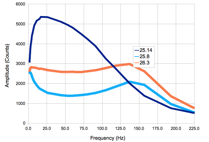
Figure: Frequency Response Disturbed By Moisture. These transmitters previously showed square waves while implanted
Transmitter No5, which has acrylic coating on its amplifier, generates a 5-Hz square wave when its leads are open-circuit and when they are shorted together. We connect both leads to our 20-MΩ source. The oscillations continue, but with a 15-Hz input, the frequency shifts to 15 Hz. With only X+ connected, or only X− connected, this shift does not take place. Transmitter No14.9 has nominal response, No14.11 has high gain at 60 Hz, No14.13 has high gain at 40 Hz. We put all ten tranmitters in the oven.
[07-NOV-13] After a one-hour bake at 60°C No5 no longer square waves. It picks up mains hum and heartbeat. Battery voltage is 2.7 V.
[18-NOV-13] After three days in water, we test 30.1 through 30.14. Transmitters 30.2 through 30.14 have frequency response within 1 dB of nominal. Transmitter 30.1 is 2 dB lower than nominal at the high end, but still acceptable. No square waves. We ship the prettiest ones, which is all but 30.2 and 30.4.
Transmitter No5 (mis-labeled) won't turn on, even though it cannot possibly have run down its battery by this time if it were fully functional.
[26-NOV-13] We have a new batch of fourteen A3019Ds encapsulated. These we made with water-soluble flux only, so that we washed the circuit after loading the battery, blew dry, and baked. We applied acrylic coating to the amplifier. All turn on and off easily. Perform the harmony and heartbeat test and all function well. Leave them to soak.
[01-DEC-13] Remove the new batch of fourteen from water after five days in water. Measure frequency response of all fourteen, and all are within ±0.5 dB of nominal except at 140 Hz, where they are within ±1 dB. Transmitters 29.1 and 29.2 show poor reception. We measure their transmission bit period to be 191 ns rather than the nominal 200 ns, and this is sufficient to cause drop of samples occasionally with the A3018C. We place them all in water and measure switching noise. Eleven show normal switching noise, but 29.5, 29.7. and 29.12 have switching noise with fundamental harmonic amplitude 30 counts (as opposed to the usual 5-20 counts) with harmonics all the way up to 100 Hz (as opposed to no such harmonics). We bake them for an hour at 60°C. When we take them out they show no noise, but after a minute cooling down in water, they start up again. The rms noise on 29.5, 29.7, and 29.12 is 38, 37, and 35 counts rms, which is only slightly higher than the usual 30 counts rms. What is unusual is the higher harmonics, which result from spikes in the switching noise. We place in water at 40°C. The amplitude of the first harmonics drops to 10 counts.
[04-DEC-13] Transmitters 29.1 and 29.2 perform well at 37°C. We ship 29.1, 29.3, 29.4, 29.6, 29.8, 29.9, 29.10, 29.11, 29.13, and 29.14 to make a set of ten. Transmitters 29.5, 29.7, and 29.12 still show the same spikey switching noise.
[05-DEC-13] Transmitter 29.2 performs perfectly at 20°C today. Noise still present on 29.5, 29.7, and 29.13.
[24-DEC-13] Transmitters 29.2, 29.5, 29.7, and 29.12, 30.4 and 26.3 have been soaking in water. No square waves.
2014
[01-JAN-14] Still no square waves. We modify the firmware to produce source code P3019A03.able, which ensures 50% mark-space ratio for the transmit clock, at the expense of less resolution in the transmit clock period. For a plot of reception efficiency versus clock period with 50% mark-space ratio for the Octal Data Receiver (A3027C) see here, but note that this graph was obtained with Subcutaneous Transmitter (A3028) devices rather than with A3019s. The RF transmission in both devices is identical.
[13-JAN-14] Transmitters 29.2 and 30.4 give perfect reception and frequency response. Period of transmit clock for 29.2 is 194 ns and 205 ns for 30.4.
[27-JAN-14] We have a batch of 13 A3019Ds that have been soaking in water for three days. No31.6 has switching noise 20 μV. The one marked 31.1 has ID number 14. The other eleven are good.
[12-FEB-14] Transmitters 29.5, 29.7, and 29.12 have been running continuously since 01-DEC-13 and are still going strong.
[19-FEB-14] According to ION, transmitters 29.1, 29.6, and 29.10 have "failed after about 2 weeks of normal recording." These were encapsulated on 26-NOV-13. "All three transmitters started to generate a square wave."
We go through twenty broken A3019 circuits looking for ones we can repair. We replace half a dozen U2s and one U1. We encounter four transmitters that usually turn on with nominal quiescent current, but occasionally turn on with hundreds of microamps of quiescent current. They still operate properly at this higher current. We caught this problem in these transmitters, but it's possible some made it through our quality control and were encapsulated.
[21-FEB-14] We receive recordings from ION of the three failed transmitters and there are no square waves, just what appears to be 100 μV noise from a damaged RF transmitter.
We have a new batch of 11 A3019As encapsulated. This batch we made with water washing after the battery load, starting the transmitter with tweezers, baking, and acrylic coating. What's new is making sure we start up the transmitter with tweezers after the water wash. No37.3 won't turn on. The remaining 10 we turn on and place in water. Switching noise spectrum is shown here. The peak amplitude is 6 μV, which is normal, so we have no of the noisy transmitters.
[21-FEB-14] Transmitters 29.5, 29.7, and 29.12 have been running continuously since 01-DEC-13 and are still going strong. We turn off 29.7 to send to Edinburgh along with 31.6.
We look again at the layout of he A3019 to see if we can understand how switching noise and square waves arise. The XA signal is X amplified by one hundred. It appears ona via that is 0.6 mm from the R9 pad that carries X. We take an applicator with a 2-mm tip, wet it with tap water, and place it between the XA via and the X pad of R9. We immediately see a square wave on X, of frequency 1-5 Hz. We place the swab between the VA via and R9 and we see noise on X of frequency around 20 Hz, which is consistent with Switching Noise. This noise is present on the VA.
[24-FEB-14] We have 10 A3019As in water. All turn on and off easily except No37.7, which is hard to turn on. No square waves. We change the room-temperature water for ice-cold water in order to provoke condenstaion within the encapsulation.
[26-FEB-14] We have 10 A3019As that have been soaking for five days, including an ice-cold water exchange. No37.6 and No37.7 have some trouble turning on and off. Measure frequency response. No37.1, No37.5, 37.6, 37.7, 37.8, 37.12, 37.13, and 37.14 have nominal frequency response. No37.2 and No37.4 have −6 dB gain but nominal shape to frequency response. We apply sine wave through 50 Ω and low gain persists in both transmitters. We bake for 30 minutes and gain in both returns to normal. We measure the in-water noise spectrum of all ten transmitters is shown here. We put all transmitters in the oven to bake for 30 minutes. Upon removal, all transmitters have correct gain and frequency response. No37.6 and No37.7 are hard to turn on when they are cold. We check their RF spectra and they have peaks at 915 MHz and 916 MHz respectively. A large mains hum signal in No37.6 clips at about 75% of full scale, but all others give full-scale mains hum easily. We decide to ship to Oxford on Job 1146 No37.1, 37.2, 37.4, 37.5, 37.7, 37.8, 31.11, 37.12, 37.13, 37.14 making a set of ten.
[07-MAR-14] We receive transmitters 29.1, 29.6, and 29.10 at ION. We place them in water and record noise, as shown below.
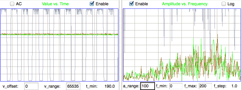
Figure: Problems from Batch Twenty-Nine. No29.1, green, and No29.6, brown, show no EEG power, insted the same high-frequency noise. No29.10, gray, has a 10-Hz full-scale square wave.
These transmitters we assembled as follows. Solder leads with acid flux, wash, dry, solder battery with acid flux, wash, dry, bake, acrylic coating on amplifier, test. It was not until the test that we tweezered R1 to start the magnetic sensor. We did not check if the circuit was on or off until we tested. We encapsulated and soaked, then measured the switching noise. Transmitters 29.5, 29.7, and 29.12 showed switching noise in the form of spikes rather than a sinusoidal oscillation. Something was wrong with the switch. We did not see this problem in any of the twenty transmitters we shipped following batch 29. Transmitter No29.10 showed exactly the same noise as No29.1 and No29.6 while implanted, but now generates a square wave.
[10-MAR-14] We place 29.1, 29.6, and 29.10 in water and measure noise. No29.10 starts oscillating at around 10 Hz, but oscillations damp down to nothing. Now all three are showing the same high-frequency noise shown above.
No29.6: We strip 5 mm of silicone from the lead tips. We drop device in water. Input noise is normal. Connect to 20-MΩ sinusoidal source. Gain versus frequency is normal.
No29.1: We strip 5 mm of silicone from the lead tips. We drop device in water. We see high-frequency noise. Connect to 20-MΩ sinusoidal source. We see zero gain at all frequencies. We cut back both leads to 40 mm and strip new tips. We drop in water. Input noise is normal. Connect to 20-MΩ sinusoidal source. Gain versus frequency is normal. The green cut-off lead is 60 mm long with resistance ∞ Ω. We find a break 10 mm from one end. No sign of excessive stretching nor any cut through the silicone at the break. The orange lead is 70 mm long and has resistance 23 Ω.
No29.10: We strip 5 mm of silicone from the lead tips. We drop device in water. We see high-frequency noise. Connect to 20-MΩ sinusoidal source. We see zero gain at all frequencies. We cut back both leads to 40 mm and strip new tips. We drop in water and noise is normal. Connect to 20-MΩ sinusoidal source and gain is +6 dB at 16 Hz and −16 dB at 90 Hz. The green cut-off lead is 70 mm long with resistance ∞ Ω. We find a break 10 mm along its length. No sign of excessive stretching nor any cut through the silicone at the break. The orange lead is 70 mm long and has resistance 31 Ω.
We take transmitter No26.11 and immerse the transmitter body and the X+ lead in water. We keep the X− lead out of water. We place the water and transmitter in a faraday cage. We see high-frequency noise. We immerse X− and input noise returns to normal. We take the X+ lead out of water. We see high-frequency noise as shown below.
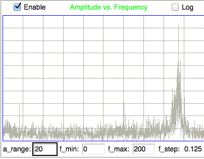
Figure: Noise we expect when X+ Lead Is Broken. We have No26.11 in water with X−, and X+ outside water.
The amplitude of the high-frequency noise is 20 counts with X+ broken, and 60 counts with X− broken. The following plot and spectrum shows the EEG baseline from No29.1, 29.6, and 29.10 on 27-JAN-14 before the problems with their recordings started.
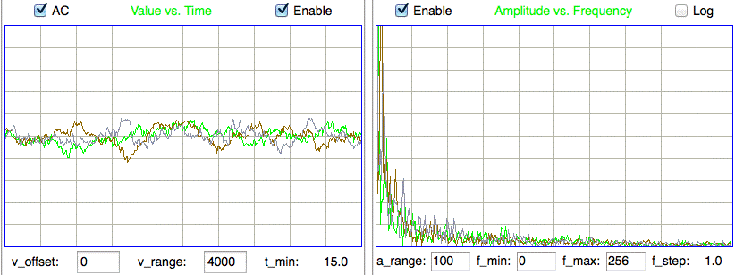
Figure: EEG Baseline for No29.1, 29.6, and 29.10 Before High-Frequency Noise Observed.
We see EEG baseline spectrum indicating no breaks in the leads, and no high-frequency noise, indicating the same.
[11-MAR-14] Transmitters No29.1, 29.6, and 29.10 all spend several hours in the oven at 60°C and dried out overnight. No29.1 and 29.6 show no high-frequency noise and pick up mains hum well. No29.10 generates its own square wave of 10 Hz when its leads are open circuit. In water, it shows normal noise. In our two hands, it picks up a clear heartbeat. We heat the transmitter with our hot air gun to 100°C for one minute. We let it cool to 60°C. It still generates a square wave with leads open circuit.
[31-MAR-14] Transmitters No29.1, 29.6, and 29.10 have been off and in air since 11-MAR-14. Today, No29.1 and 29.6 have battery voltages 2.77 V and 2.75 V, electronic noise 30.5 and 31.6 counts rms respectively. In air, they pick up mains hum. Transmitter 29.10 does not transmit.
[02-APR-14] Transmitters No37.9, 37.10, 37.11, 37.12, 37.13, 38.1, 38.2 are ready for encapsulation. All have noise below 35 counts rms. All have nominal gain except 37.9 and 37.11, whose gain is 2 dB below nominal, but shape of frequency response is correct. Reception is good for all.
[11-APR-14] Transmitters No37.9, 37.10, 37.11, 37.12, 37.13, 38.1, 38.2 have been in water for four one week, with four cycles of hot then cold water. No square waves. We measure frequency response and it is within 1 dB of nominal for all seven. All switch on and off easily. Switching noise is shown below.
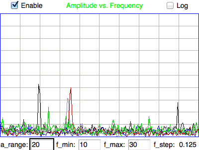
Figure: Switching Noise in Batch 38, No37.9, 37.10, 37.11, 37.12, 37.13, 38.1, 38.2. This is the final batch of A3019s we will make.
Despite the seven days of warm and cold water cycles, these seven transmitters show no sign of condensation problems.
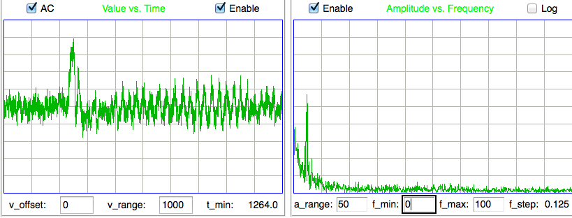