Note: The A3010A and B must warm up for ten minutes before it achieves its best performance.
The Data Receiver (A3010) is a LWDAQ device made up of two circuits and enclosed in a die-cast aluminum box. One circuit is a Demodulating Receiver (A3005C), which receives signals from transmitters such as the Subcutanteous Transmitter (A3009). The other circuit is a Data Recorder (A3007B), which takes the demodulated output from the A3005C, detects A3009-type transmissions in the random bit sequence of the output, and stores messages it detects in its memory, where they are available for to the LWDAQ through the Recorder instrument.
 Figure: Data Receiver (A3010A) with Subcutaneous Transmitters (A3009R).
A 915-MHz dipole antenna sticks out of the box, and a fifteen-foot CAT-5 cable extends from one side. You plug this cable into your LWDAQ Driver, such as the (A2037E). For instructions on how to use the LWDAQ, consult the User Manual. In particular, consult the section on the LWDAQ Recorder instrument.
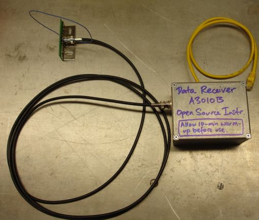 Figure: Data Receiver (A3010B) with Antenna (A3015L).
The A3010B is an upgrade of the A3010A. Instead of a dipole antenna or a loop antenna attached to the box, the A3010B provides a BNC socket, so you can plug a BNC antenna, such as the Antenna (A3015). The A3010B CAT-5 cable is shorter, so it is less bulky. The antenna cable allows you to bring the antenna close to your transmitters, while leaving the A3010B enclosure close to the LWDAQ driver. The A3010B firmware (on the A3007B) corrects an error in the A3010A firmware that caused blocked messages even with a strong signal, and corruption of messages with low signal power.
If you open up the box, you will see the two circuit boards screwed together, and to the bottom of the box, as shown below.
 Figure: Inside of Data Receiver (A3010A), showing A3005C (9), A3007B (8), test point for A3005C output (6), test point for input to comparator (5), test point for comparator output (4), 512-KByte memory chip (1), copper tape for grounding oscilloscope probe (2), local oscillator frequency adjustment (7), and crystal oscillator piggy-backed onto logic chip (3).
We recommend that you do not adjust the A3005C's local oscillator frequency. There is no way to check that you have performed the adjustment correctly, unless you have an RF power source whose frequency you can sweep through 902-928 MHz while you look at the A3005C output. The output should vary with frequency something like the figure below.
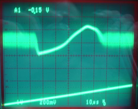
The A3010 converts the frequency-modulated signal from an SCT (A3009) into a voltage signal by means of the slope in its response with respect to frequency. It is essential that the A3005C's local oscillator be adjusted so that the response has a positive slope throughout the ISM band. This adjustment is made difficult by the fact that the A3005C's local oscillator chip warms up in the confined space of the box, and its frequency drops. We have to be sure to adjust the local oscillator frequency when the chip is at its equillibrium temperature within the box.