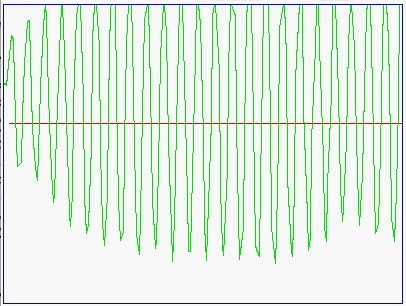
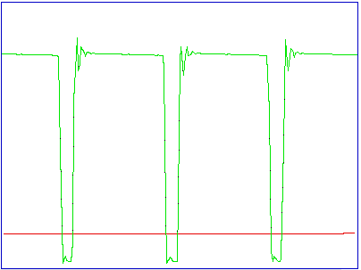
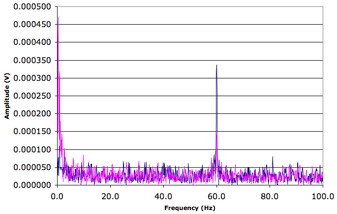
Figure: Mains Hum on ADC Input.
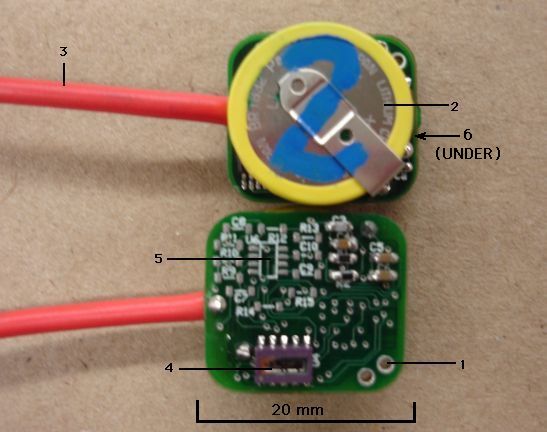
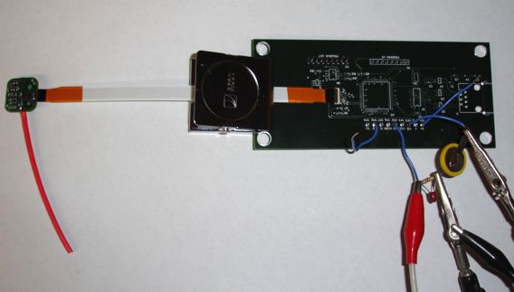
The Subcutaneous Transmitter (A3009) is 18 mm × 16 mm × 8 mm and weighs less than 4 g. The A3009A provides a differential analog input for biometric measurements. It converts its analog input into 16-bit digital samples and transmits these at 512 samples per second from beneath the skin of an animal by means of its 1-GHz quarter-wave antenna. The A3009A will operate continuously for two months on a single battery. You can de-activate the transmitter at any time with a magnet. When de-activated, the transmitter uses one fifth the power it does when it is active.
The A3009 applies a 1-GHz carrier to its antenna, and makes small changes in the carrier frequency to convey information. We say 1 GHz, but the transmitters can be programmed to operate anywhere between 850 MHz and 1050 MHz. The A3009A operates in the 902-928 MHz band.

The antenna is a quarter-wave antenna. The best length for the antenna is one quarter the wavelength of the radio-frequency signal it transmits. In air, with a 915-MHz carrier, this length is 80 mm. Beneath the skin of an animal, however, the best length is shorter, because radio waves travel more slowely in the presence of water. After much experimentation with antennas, we settled upon the bent 80-mm antenna as the best choice for operation in all environments. Nevertheless, early versions of the A3009 used straight quareter-wave antennas, and you will see such antennas in some of our photographs.
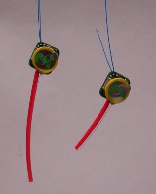
You can receive the A3009 transmissions with our Data Receiver (A3010). Here is a picture of the A3010A with two A3009Rs. The range over which this reception will be reliable depends upon the strength of local interference signals in the transmitter's operating frequency band, and upon the presence of large metal objects nearby. We get reliable reception for ranges 0 m to 2 m in our laboratory, provided we stay away from our metal tables and cabinets. In outer space, with no reflecting surfaces and no interference, the range of reception would be limited only by thermal noise. In theory, we would be able to receive signals at ranges over 200 m.
Before it can be implanted in an animal, the A3009 must be coated. Our collaborator Matthew Walker chose MED10-6607, a silicone dispersion from Nusil. You take the transmitter by the antenna and dip it in the silicone disperion, let it dry for a few hours, and dip it again. After a single coating, it is well-insulated, and after four or five coatings, it is rugged enough and smooth enough to implant.
We present the results of extensive experiments with the A3009R in our Data Transmission and Reception Circuits report.
The A3009 comes in the following versions. Some digitize and transmit the analog input. Others transmit a reference signal, which helps you determine the efficiency of transmission and reception without having to connect the transmitter to a biometric signal source.
| Version | Hi-Pass Frequency (Hz) |
Low-Pass Frequency (Hz) |
Input Impedance (MΩ) |
Dynamic Range (mV) |
Message Contents |
Message Rate (Hz) |
RF Band (MHz) |
|---|---|---|---|---|---|---|---|
| A | 0.16 | 160 | 10 | −60 to +30 | Analog Input | 512 | 902-928 |
| R | none | none | none | none | 32-Hz Square Wave | 512 | 902-928 |
S3009_1: Logic chip, 900-MHz oscillator, battery, reference clock, analog input, anti-aliasing filter, sixteen-bit ADC, and 12-way miniature programming connector. Capacitor C11 we added after discovering that C1 did not provide adequate 900-MHz decoupling for U3. We cut the connection between U5-3 and U6-3 when we found that U5 loaded R9.
P3009A: Firmware for logic chip. Same firmware, with some constant changes, works in A3009A and A3009R versions of the transmitter.
Connector: The miniature connector that makes it possible for us to build, program, and test the A3009 without a programming extension. Our previous transmitters all used an additional printed circuit board area, which we would subsequently chop off, for a programming and test connectors. The FH19S-12S-0.5SH from HRS is only 8 mm long, 3.5 mm wide, and 0.9 mm high.
Cable: The 0.5-mm pitch, 12-way, 0.3-mm thick flex cable that mates with the FH19S-12S on the transmitter board. This cable will connect the transmitter to its programming board.
Programming Board (A3011): Carried logic chip programming signals to the transmitter, and brings test signals out of transmitter for observation.
For a description of the A3009's message encoding, see here, and at the logic chip firmware. In this manual, we restrict ourselves to discussing the A3009 output spectrum, knowing that its message encoding is equivalent to modulation of its output frequency at 5 MHz.
Initial Spectra: Here we see the radio frequency spectrum obtained by the RF Spectrometer (A3008) when we turne on the first A3009, before we discovered that adding C11 increased the power output by 6 dB. The A3009 has a five-bit DAC (digital to analog converter) made of five logic outputs and five resistors (1kΩ, 2kΩ, 4kΩ, 8kΩ, and 16kΩ). One end of each resistor is tied to a logic output (0 V or 1.8 V). The other ends are tied together at the TUNE input of the VCO (U3). We control the VCO output frequency by choosing a number between 0 and 31 for zero-bit transmission, and another number for one-bit transmission. The red spectrum is what we get when we choose 0 and 15 respectively. This is the spectrum produced by the A3006, as you can see here. The green spectrum is what we get when we set both numbers to 18. There is only one peak. The blue spectrum is what we get when we pick 14 and 19. The spectrum fits nicely between the orange lines that mark the passband of our 947.5 MHz SAW filters. When we combine this modulation with a modified A3005 receiver, whose frequency response in the pass band looks like this, we see digital reception, with transitions taking place in less than 100 ns.
Transmitter and Reference Spectra: We compare the spectrum of our reference Modulating Transmitter, when driven by a square wave of 2 MHz, to that of our A3009, whose bit rate is 4 MB/s.
Reception by A3005B: This is what we see in the A3005B during reception from an A3009 at close range. The upper trace is the demodulated output from the receiver. You can see interference and noise returning as soon as the A3009 transmission is complete. The middle trace is the IF signal just before the discriminator. You can see the change in IF frequency from logic 0 to logi 1. The lower trace is the transmission bit stream directly from the logic chip on the A3009, via the Programmer (A3011). We use this direct signal as our trigger, or else there is no way to trigger the oscilloscope on the transmission in amongst the prevalent interference and noise.
The above spectrum shows power outside the ISM band. The spectrometer measures maximum power received in its measurement interval. The power outside the ISM band is caused by the start-up of the transmitter. For the first few hundred nanoseconds, its output frequency is indeterminate. Here is the raw data from the Spectrometer tool.
In the above spectrum we see that rotating the transmitter by ninety degrees reduces the received power by 15 dB. The power at range 500 cm is also 15 dB lower than the power at range 60 cm, with the same antenna orientation. We expect an inverse-square loss of power with range, so going from 60 cm to 500 cm we expect a -18 dB drop in power. We get good reception at range 500 cm, provided that we don't interpose ourselves between the transmitting and receiving antenna.
We subsequently discovered that soldering a 100-pF capacitor across the power pins of U3 (see schematic) increased the transmitter output power by 6 dB, as shown below.
With C11 installed, we obtained unreliable reception of the A3009R transmission at up to 6 m, compared to reception up to 3 m without C11. With C11 installed, we find the A3009R transmits as much power as our Modulating Transmitter (A3001A).
In the A3009 firmware, which configures its logic chip, there are two parameters that set the center frequency and modulation width of the A3009 transmission.
frequency_mid=8; "Average of 0 and 1 transmission frequencies"
frequency_range=1; "Deviation from mid frequency."
The frequency_mid gives the A3009 5-bit DAC value at which its MAX2624 transmits 915 MHz at 20°C. The A3009 adds frequency_range to frequency_mid to obtain its one output frequency, and subtracts frequency_range to obtain its zero output frequency. After more experience with the A3009, we will be able to decide upon an optimum, fixed value for its frequency range, and use this value for all transmitters. But the MA2624 voltage-controlled oscillator that generates the A3009's radio-frequency carrier has its own frequency offset with respect to its input TUNE voltage. According to the manufacturer's data sheet, the frequency response shown here moves by ±10 MHz from one chip to the next. So we must measure the output frequency of the VCO and set frequency_mid to center the transmitter's carrier frequencies within our chosen radio-frequency band. In the case of the first two batches of A3009s we made, this was the ISM band, 902-928 MHz.

Before we calibrate an A3009, we calibrate an A3005C by sweeping the frequency of our modulating transmitter through the ISM band and noting the A3005C output voltage that corresponds to the center of the band.
We determine frequency_mid by setting frequency_range to zero and watching the output from our calibrated A3005C. We edit the A3009 firmware, compile it, program the A3009 with the help of an SCT Programmer (A3011), trigger an oscilloscope using a test pin on the programmer, and watch the A3005C output. When frequency_mid brings the A3005C output close to the same output it produces when excited by a frequency in the center of the ISM band, we know that we have set frequency_mid correctly.
After we set frequency_mid, we set frequency_range to a value between 1 and 3. Here are the power spectra we obtain from transmitter 5 from batch 2 for these three values of frequency_range. The raw data is here. The A3009 is modulating its output frequency at 5 MHz.
Each DAC step up corresponds to a roughly 4 MHz increase in output frequency. With frequency_range set to 1, our one frequency is 8 MHz higher than our zero frequency. We can adjust the center frequency in 4 MHz increments. As you can see from the spectrum, the center frequency of the transmission is slightly lower than 915 MHz. A better value for frequency_mid is 9 instead of 8. When the range is 1, the spectrum is about 15 MHz wide. With range 2, it expands to 20 MHz. Because the spectrum is not centered perfectly, some of it extends outside the ISM band and would be rejected by the ISM-band SAW filter in an A3005C receiver. When the range is 3, the spectrum is roughly 25 MHz wide.
As the frequency range increases, so does the amplitude of the signal produced by the A3005C in response to the transmission. We displayed the A3005C output on the oscilloscope top trace, and the one-zero logic output from the A3009 on the lower trace. We took photographs of the oscilloscope display for frequency ranges one, two, and three. The amplitude of the received signal almost doubles when we increase the frequency range from 1 to 2, but we see only a small increase in amplitude when we increase the range further to 3. The RF signal for range 3 extends beyond the ISM band, and we see the response appears to slow down.
After completing our experiments with omni-directional antennas, we tested the operating range of the A3009 with frequency ranges 1 and 2. We noticed no difference in range. We decided to use frequency_range = 2. The signal we get from the receiver doubles in amplitude when we use the ±8 MHz modulation. The modulation bandwidth increases by only 5 MHz to 20 MHz. We can now tolerate a larger shift in the transmitter's center frequency with respect to the receiver's center frequency, because the two modulation is broader. At the same time, we find that our SAW filter pass bands are at least as wide as the 902-928 MHz band, so we have room for the edges of our modulation bandwidth.
Here is our apparatus for monitoring A3009 current consumption. We use a Input-Output Head (A2057 connected to the battery voltage and to the voltage drop across a 1 kΩ resistor in series with the battery's negative terminal. We used the LWDAQ software's Acquisifier to measure the two voltages, check for any transmissions with a Data Receiver (A3010), and write the results to a file. We instructed the Acquisifier with an Acquisifier script.
Our first batch of six A3009s drained their batteries at random. They would work for a few days, and then the battery would go flat. This happened to the two transmitters we sent to ION (transmitters 1.2 and 1.3), as well as one we had here (transmitter 1.1). We took another transmitter from the same batch of six, and monitored its current consumption over a weekend. This one we identified by a green paint dot on its bottom side.
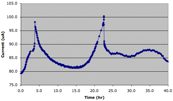
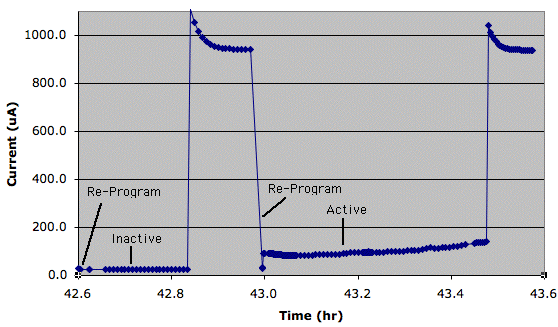
As you can see, the active current consumption varies from 80 μA to 100 μA. Then, it suddenly jumped up to 1 mA, as shown below.

After a half-hour at 1 mA, during which the transmitter continued to transmit its reference square wave, the current dropped all by itself to 30 μA and the transmitter was inactive. In this state it remained for about ten minutes, and then its consumption jumped up to 1 mA again, while the transmitter remained asleep.
We observe similar current consumption problems with other transmitters from the first batch of six. When we remove the VCO and other components from the board, leaving only the logic chip, we still observe the same problems. We conclude that it is the logic chip that is causing the problems.
We then recalled how we had heated the six logic chips of the first batch all together, at the same time, for almost a minute, with the heat gun only inches from the chips. Such treatment far exceeds the manufacturer's absolute maxima for package heating, and we believe it is possible that we damaged the chips by over-heating them.
We found that the high current consumption could be reversed temporarily by re-programming the logic chip.
When we received transmitters 1.2 and 1.3 back from ION, we found the current consumption of 1.2 was around 1 mA even after re-programming, while the current consumption of 1.3 appeared normal in the short term. Over the long term, however, transmitter 1.3 showed the same variation in current consumption we saw in our One Green Dot transmitter. We conclude that the transmitters that failed at ION suffered from the same malady as all transmitters in Batch One. Sooner or later, its current consumption will rise to 1 mA, and it will drain its battery.
We made another batch of eight transmitters, this time heating the chips individually, and with more care. The current consumption of the second batch was stable.
With the eight transmitters from our second batch, we measured the current consumption of the various parts of the A3009, in both the active and inactive state.
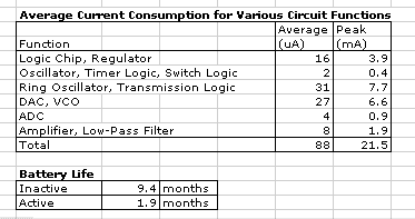
With a 120-mA-hr battery capacity, we expect an operating life of 2 months, and a shelf life of 9 months.
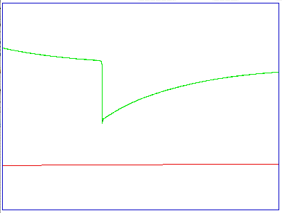
We connected a fresh battery to transmitter 2.3, which is fully-populated. Because the transmitter was plugged into its programming board, using the battery on the programming board, it picked up mains hum through the 6-inch flex connector joining it to the programming board, and we were able to watch this mains hum to see that the transmission was working properly. We measured the current consumption and battery voltage every six hours, with one or two breaks of a day along the way. Here is the graph of the battery voltage versus time for the time for which the transmitter was digitizing and transmitting the mains hum signal.

As you can see, the battery life is approximately 1300 hours, or 1.8 months. Transmitter 2.3 has quiescent current 94 μA, so the total current drain from the battery was 120 mA-hr, which is equal to the advertized capacity of the battery.
We also note from the graph that the transmitter appears to work properly down to a supply voltage of 2.2 V.
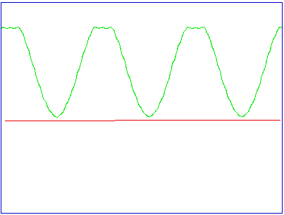
The A3009A transmits the voltage on the CH0 input of its ADC. The ADC converts CH0 into a 16-bit number, where number 0 is voltage 0V on the schematic, and number 65535 is voltage 3VA. The difference between 3VA and 0V is the battery voltage, which drops from 3 V down to 2.2 V during the life of the transmitter. To test the dynamic range of the ADC, we touched pin U5-3 before we had soldered on U6, and obtained the following picture of mains hum in the Recorder.
With the remaining analog parts attached, we connected our function generator across X+/X−. Capacitor C9 (100 nF) AC-couples the differential input onto R9 (10 M&Omega), and shifts the input's common-mode voltage to VCOM, which is 1.8 V irrespective of the battery voltage. We expect the time-constant of this AC coupling to be roughly 1 s (C9 × R9). We applied a slow square wave to the X+/X− input, and recorded the following reponse.
The response covers 20 kBytes of data uploaded from the driver, which is 2000 samples from the transmitter and 500 time stamps. The 2000 samples cover 2000/512 ≈ 4 s. The time constant of the step response appears to be around 1 s.
We applied an 80-Hz sine wave to the input, and observed clipping on the top side, as shown above. The height of the display represents 2.8 V, which is the battery voltage we measured on the transmitter. The clipping takes place at about 2.5 V, which is only 0.7 V above VCOM. The OPA2349 can drive its outputs to within at least 300 mV of its supplies, but typically 150 mV. What we see here is the onset of clipping at U6 pin 7. If we increase the size of the sine wave, we can force the ouput higher, but we see some distortion of the signal. The dynamic range of the analog input extends farther downwards than it does upwards. This allows us to record larger asymmetric waveforms than we would otherwise be able to accommodate, as we see below.
If we assume that clipping takes place at 0.3 V and 2.5 V, our dynamic range is from VCOM−1.5 V up to VCOM+0.7 V at the ADC. To determine the dynamic range at X+/X−, we need to know the gain of the amplifier.
We applied a 10-Hz, 20-mV peak-to-peak sine wave to the analog inputs. The output as seen on the Recorder screen was 600-mV peak-to-peak. The gain of the amplifier appears to be ×30. By design, it should be ×28. The difference is because our Recorder software assumes that the battery voltage is 3.0 V, when in fact the battery voltage was only 2.8 V. When we account for this error, the design and measured gains are the same. With a gain of 28, and the dynamic range we measured at the ADC, the dynamic range at the analog input becomes −50 mV to +23 mV.
We applied a 20-mV peak-to-peak sine wave again, and varied the frequency of our sin wave to obtain the frequency-response of the three-pole low-pass filter implemented by U6. Consult our Filter Design Guide for a description of this circuit and other filters, and for an Excel spreadsheet tool that will allow you to calculate the theoretical frequency response of the transmitter circuit. The figure below gives both the theoretical response and the response we measured.

We are surprised at the close agreement between the measured and designed frequency response. We expected a similar-shaped response, but an offset in the cut-off frequency due to the inaccuracy of the 1-nF capacitors we used in the circuit. But the 10% 1n0 capacitors must have been within 1 % of 1 nF, because the two curves follow one another to within a few Hertz. The cut-off frequency is the frequency at which the gain drops by 3 dB, and that's around 160 Hz.
We sample the analog input at 512 Hz, so we must eliminate all frequencies above 255 Hz if we are to avoid aliasing completely. Our filter attenuates 256 Hz by 16 dB with respect to 1 Hz. It attnuates 400 Hz by 30 dB. If the attenuation at 256 Hz is inadequate, we can move the filter's cut-off frequency down from 160 Hz to 100 Hz. This will increase the attenuation of 256 Hz from 16 dB to 30 dB.
We soldered X+ and X− together. This shorts out thermal noise in R9. We reduced the range of the display from 3 V to 5 mV and switched on the display's AC coupling.
What we see in the noise plot is noise generated by U6 on pin 2, mains hum induced in the leads from X+/X− to R9, and digital signal noise coupled onto the analog signals from the transmission burst. The noise is equivalent to 20 μV rms at X+/X−. According to the manufacturer's data sheet, the OP2349 voltage and current noise together will combine to generate less than 6 μV of noise in our 160-Hz bandwidth. We don't see clear signs of mains hum in the noise. We assume that the 20 μV of noise is digital signal noise.
We removed the short between X+ and X−, and replaced it with a 10 MΩ resistor. The noise looked the same, with amplitude 600 μV at the ADC. The thermal noise generated by the two 10-MΩ resistors in parallel is roughly 3 μV in our 160-Hz bandwidth. This noise is insignificant compared to our circuit-generated 20 μV of digital noise.
The A3009A firmware uses the lower four bits of the ADC word to generate a transmission time offset for each sample transmission. One 16-bit ADC count represents 50 μV at the ADC input. Our noise is 600 μV, or ±12 counts rms, which is enough to create a good random number in the lower four bits of the ADC sample.
To waterproof the A3009, we dip it in MED10-6607 silicone dispersion coating.
As you can see in the above figure, the silicone dispersion drips slowly down the antenna. We coated transmitters 2.2 and 2.7 five times, to make sure that they were water-proof. After five coates, they were a little fatter than they are supposed to be. We believe that we can get by with only two coats, if we leave the transmitter in the dispersion for a few minutes before removing it. By leaving it in the dispersion for a few minutes, we allow air bubbles to emerge from the space between the battery and the circuit board, so that the components will be coated properly.
We coated transmitter 2.4 twice and then put it in water, where it worked well. Afterwards, however, we noticed that it kept turning itself on, from which we concluded that water had penetrated under the silicone to the reed relay. The next day, 2.4 was trasmitting a weak and garbled RF signal. We conclude taht two coats is not enough. We will dip five times in future.
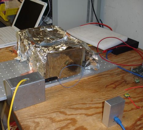
Praveen Taneja of Brandeis University connected the X input of an A3009A to two points roughly 10 mm apart just within the skull of a live mouse. He used 50-μ diameter stainless steel wire soldered to silver screws inserted through the skull. The wires were roughly 100 mm long, and folded up randomly over and around the transmitter during our experiment. The mouse was only 50 mm long, so Praveen did not attempt to insert the transmitter into the mouse's body. Instead, he glued the transmitter to the top of the mouse's head, over the electrode connections, with a mixture of dental cement powder and super-glue. He buried the RF antenna beneath the skin on the mouse's back and neck, so that it was entirely enclosed. We allwed the mouse one day to recover from surgery.
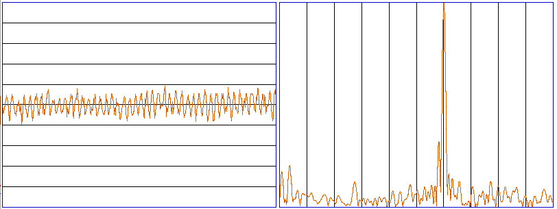
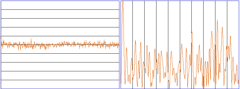
Praveen brough the mouse the Brandeis University HEP basement, where we started the transmitter and began to record data. We saw 60-Hz mains hum. In anticipation of this experiment, we prepared the first version of the Neuroarchiver to obtain the fourier transform of recorded signals. Below you see the Neuroarchiver output for the noisy signal.
At Praveen's suggestion, we wrapped aluminum foil around four sides of the mouse's cage, and placed an aluminum plate beneath.
These precautions dramatically reduced the mains hum on the transmitted signal.
With or without mains hum, however, transmission from the mouse was reliable. As the mouse moved freely around the cage, we never lost more than one out of every hundred transmitted samples. We assume these losses were due to the mouse orienting itself in small reception dead spots, but we are not sure. We conclude that the A3009 transmission is reliable from beneath the skin of a moving animal.
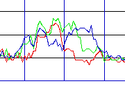
Praveen tells us that his usual mouse EEG signals are of order 20 μV rms. The A3009 has insufficient gain to detect a 20 μV signal. The rms noise on the input is 22 μV. We don't expect to be able to see EEG signals clearly with our A3009, but we might be able to pick our EEG activity in the power spectrum.

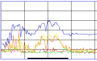
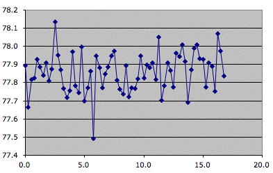
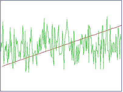
Praveen's work with mice involves monitoring EEG power in the Delta Band (1.5 Hz to 6 Hz) at the same time as EMG amplitude. An increase in EEG Delta Power at the same time as a decrease in EMG amplitude is well-correlated with NREM (non-rapid eye movement) sleep. When the mouse is REM (rapid eye movement) sleep, it's brain activity is similar to its waking brain activity. The graph above shows the variation in EEG Delta Power we observed with the A3009. Whether this power was noise from an ambient electrostatic field, or from nerve activity in th mouse, or some combination of the two, we cannot say. We were unable to correlate the rises and falls in Delta power with any EMG input, because we did not monitor EMG. We monitored motions of the mouse with our camera, as you can see here, but our motion detection does not correspond to the same time period as our EEG recording (this was not due to incompetence, but negligence).
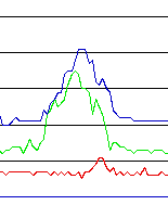
As we mentioned above, we used teflon-insulated stainless steel wires to connect the A3009A to the screws through the mouse's skull. We soldered the wires into the A3009A contact holes. The solder did not wet the stainless steel, so that the stainless steel passed straight through the solder filling the contact holes without any melding of the wire with the solder. Such a joint is called a cold joint. A cold joint gives us electrical contact simply because the two wire and the solder are in physical contact. A warm joint gives us electrical contact because the material of the wire and the solder have joined into one continuous metal body. In our experience, and that of Matthew Walker and others, cold joints are unreliable and noisy. Fluid and air penetrate the joint and oxidise the metal surfaces. The oxides are not conducting, so the joint can stop conducting, or it can be intermittent with mechanical force. Once the resistance of the joint rises, the oxide layers act like rectifiers, as in the old cat's whisker diode used in early crystal radio sets. A colleague of Matthew Walker's claimed that his cold joints once rectified and received an AM radio station.
Matthew Walker was certain that stainless steel joints, unless soldered with the correct acidic flux, would generate noise of the type shown in the Delta Power graph above. He recommends using silver wire, which solders well and is resistant to corrosion.
Matthew Walker also recommended making connections to the brain without soldering. One method is to run the silver wire through a hole in the skull, and allow the bare tip to penetrate the brain. You hold the wire in place by turning a screw into the hold. Another method is to use an electrode that passes through a very thin hole, and provides a crimp at the top for a crimp-contact with a silver wire. Our suggestion was that we solder the silver wire to a gold-plated pin, which we can press into a tight hole in the skull in the presense of a drop of super-glue to secure it in place. The tip of the pin is rounded, and makes contact with the brain.
Matthew claimed that the mains hum we observed on our mouse EEG before we shielded the cage was due to the high resistance of our ground electrode. We used two electrodes of the same sort: stainless steel wires soldered to silver screws. He says these contacts have resistance at least 100 kΩ. As we show in our study of mains hum, a high resistance to our circuit signal ground from the signal source will result in more mains hum. For his ground terminal, Matthew uses a 20-mm length of bare silver wire. At one place he twists it around a screw in the animal's skull, to secure it. Low-resistance contact is made by the 20-mm wire touching the skin and inner organs along its entire length.
We resolved to test Matthew's ideas, and our own, in another aminal experiment.
If we probe the A3009A signal path with an oscilloscope, we find that the dominant source of noise is at the ADC input. With more gain in the signal path, the signal will be larger in proportion to this noise, and so reduce the effective noise at the input. Because of offsets in the A3009's OPA2349.pdf, we are unable to increase the signal path gain without adding another amplifier. We resolved to design a new transmitter with higher analog gain, and arrived at the A3013.
The following table gives the firmware constants we used in each of the A3009A transmitters we made, and their quiescent current. The quescent current of a fully-populated board when transmitting (awake) is the same whether it is programmed as a reference or analog transmitter. If it is a reference transmitter, it ignores the ADC output, while continuing ADC conversions, and generates an artificial square wave. If it is an analog transmitter, it transmits the ADC conversion, and uses the lower four bits of this conversion to displace its transmission instant.
| Name | Transmit ID |
Mid Frequency (Counts) |
Frequency Range (Counts) |
Function | Sleep Current (μA) |
Wake Current (μA) |
New Battery | Comment |
|---|---|---|---|---|---|---|---|---|
| 1.1 | 1 | 7 | 2 | Reference | 20 | 86 | 05-MAY-06 | All Parts, Faulty U2 |
| 1.2 | 2 | 9 | 3 | Reference | 20 | 78 | 05-MAY-06 | No ADC, Faulty U2 |
| 1.3 | 3 | 7 | 3 | Reference | 21 | 81 | 05-MAY-06 | No ADC, Faulty U2 |
| 2.2 | 2 | 8 | 3 | Reference | 17 | 78 | 24-MAY-06 | No ADC, Five Coats, No C11 |
| 2.3 | 3 | 8 | 2 | Analog | 24 | 94 | 14-SEP-06 | Battery Life Measurment Mouse Experiment |
| 2.4 | 4 | 9 | 2 | Reference | 21 | 79 | 13-JUN-06 | Two Coats, Damaged by Water |
| 2.5 | 5 | 8 | 2 | Analog | 91 | 160 | - | Logic Chip Gone Bad High Sleep Current |
| 2.7 | 7 | 8 | 3 | Reference | 17 | 77 | 24-MAY-06 | No ADC, Five Coats, No C11 |
| 2.8 | 8 | 9 | 2 | Analog | 19 | 83 | - | Taking to England |
| 2.9 | 9 | 7 | 2 | Analog | 18 | 88 | - | Taking to England |