Demodulating Receiver (A3005B/C)
© 2005-2007, Kevan Hashemi,
Open Source Instruments Inc.
Contents
Description
Development
Performance
Signal Identification
Conclusion
Description
The A3005C is a modified version of the A3005A. The A3005A was the receiver used in Stage Two of our Subcutaneous Transmitter development, the A3005C is the version used in Stage Three. The A3005B is an intermediary between the two. The schematic for all versions is the same, but some parts change. For the A3005B and A3005C, we increased the gain in the signal path by a factor of 20 (23 dB). For the A3005C, we switch the reception band to 902-928 MHz. The A3005A and A3005B operated in the 930-970 MHz band.
S3005_1: SAW Filter and Downshifter for A3005A. The A3005B and A3005C change U2 and U3 to ERA-3SM (or MAR-6SM). These amplifiers together add 20 dB gain to the signal path. The A3005B LO frequency is 1020 MHz instead of the A3005A's 1000 MHz. The increase in LO frequency shifts the 930-970 MHz SAW filter passband with respect to the 50-MHz resonant frequency of the IF discriminator. The pass band of the SAW filter now appears in IF range 90 MHz down to 50 MHz. (We say down to because 970 MHz gets downshifted to 50 MHz, and 930 MHz gets downshifted to 90 MHz.) The A3005C changes L5 to the B3588, which is a 900-930 MHz SAW filter. The A3005C LO frequency is 985 MHz, so that the SAW filter pass band appears in IF range 85 MHz down to 55 MHz.
S3005_2: Limiting Amplifier (U7, U8), Discriminator (R19+L8+C22 and R24+L9+C26), and Demodulator (U9, U10) for A3005A. The four OPA699 limiting amplifier chips are mis-labeled "OP699". The A3005B and A3005C change R16 to 1 kΩ, thus boosting the signal path gain 3 dB.
Before we describe the behavior of the A3005B, we will treat you to a description of its development.
Development
When we use an A3005A with the A3004 or A3006, we find that the A3005A output saturates during the transmission of a logic 1, and shows noise or interference during a logic 0. A 1 is the presense of 950-MHz RF power on the antenna, and a 0 is the absence of 950-MHz RF power. The A3004 and A3006 transmit 875 MHz to indicate a zero, but the receiver discards the 875-MHz power. We conclude elsewhere that we should design a new transmitter that transmits at two frequencies offset by 10 MHz from the SAW band center frequency. For the A3005A with a DSF947.5 SAW filter, these two frequencies would be 937.5 MHz and 957.5 MHz.
We now offset the A3005A LO frequency so that the dual LC tank circuits cause a variation in receiver output across the passband of the SAW filter, as shown below.

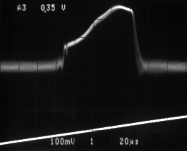
Figure: Response versus Input Frequency. The top traces are the receiver output, and the bottom trace is the transmitter's VCO input. The left side is for LO of 1000 MHz, and the right side is for LO of 1020 MHz.
We would like the change in receiver response to be sharper, so that we will be less vulnerable to holes. We can make the LC tank circuits sharper by increasing resistors R19 and R24. These resistors are each 100 Ω in the original A3005A design.
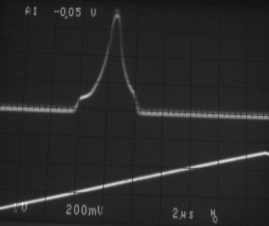
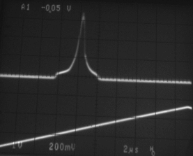
Figure: Sharper Receiver Variation. The top traces are the receiver output, and the bottom trace is the transmitter's VCO input. The left side is for R19 and R24 equal to 500 Ω, and the right side is for 1 kΩ.
A hole in the reception now looks like this:
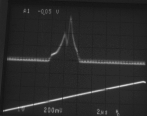
Figure: Hole in Receiver Response. The top trace is the receiver output, and the bottom trace is the transmitter's VCO input. Resistors R19 and R24 are 500 Ω We move around until we see this hole appear from a reflection.
When we offset the LO frequency once again to 1020 MHz, we get the receiver response shown below.

Figure: FM Demodulation Response. The top trace is the receiver output, and the bottom trace is the transmitter's VCO input. Resistors R19 and R24 are 500 Ω The local oscillator frequency is 1020 MHz.
We find that we can modulate the transmission frequency at up to 4 MHz, and see a square wave in the receiver output. The tank filter rings after it has been excited with its 50-MHz resonant frequency. This ringing increases as the LC peak gets sharper. So we find that the steeper the change in response with frequency, the more ringing we get in the output, and therefore the slower our maximum bit rate.
For the A30005B, we reverted to the original 100-Ω resistor, to create a sharp change in response in the middle of the pass band, but a relatively constant response on either side of the middle. We increase the signal path gain to the point where the IF amplifiers are saturating with the thermal noise generated in the antenna. It is now almost impossible to create a hole in the receiver response, because even with 99% power loss, we still have enough power to saturate the IF amplifier and obtain a clear signal.
With an extra 38 dB of gain, the A3005B's amplifies its antenna noise to a 1-V, amplitude-limited signal at the output of its IF amplifier (U8 pin 6).
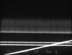
Figure: Amplified Antenna Noise. Upper trace is demodulated output, middle trace is limiting IF signal, sloping trace is the TUNE input to our Modulating Transmitter 70 cm away.
In the figure above, we see amplified antenna noise in the upper trace, as it appears on signal D, the demodulated output of the A3005B. The center trace shows the signal at the IF amplifier output, just before the discriminator. To obtain these traces, we covered the A3005B antenna with foil, while at the same time running our Modulating Transmitter (A3001A) 70 cm away on the same table, and driving it with a TUNE signal given by the lower sloping trace in the figure. We can see some sign of disturbance in the thermal noise output when the TUNE voltage passes through the range where the Modulating Transmitter's frequency lies within the A3005B's SAW filter pass band. But this disturbance is minimal, so we are confident that all we are seeing in the A3005B output is antenna and amplifier noise.
We now take the foil off the A3005B antenna, and we immediately see the Modulating Transmitter output within the SAW filter passband.
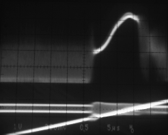
Figure: Amplified Interference and Modulating Transmitter Signal. Upper trace is demodulated output, middle trace is limiting IF signal, sloping trace is the TUNE input to our Modulating Transmitter 70 cm away.
As we sweep our Modulating Transmitter frequency through the 947.5-MHz SAW filter pass band, we see the IF amplifier get slighthly larger, but not much larger. The demodulated output, however, becomes sharp and noise-free. The Modulating Transmitter signal is dominating both noise and interference to create a clear signal, and show us the frequency response of the discriminator. When the Modulating Transmitter signal is outside the SAW filter passband, the IF output is saturated as it was in the previous figure, but this time it is not electrical noise that is saturating the amplifier. The appearance of the demodulated output is different, and changes as we cover the antenna. This difference is not obvious from the two oscilloscope pictures, but it is obvious when you cover the antenna, and watch the traces. What we are seeing here is amplified interference from other signal sources in the SAW filter passband.
Two years after we made the first A3005C and recorded most of the observations in this report, we developed the Data Receiver (A3010B) Version B, in which the A3005 antenna connection is a BNC socket. The BNC socket allows us to connect the A3005C to an antenna such as the A3015, or directly to a source of RF power. We took a Modulating Transmitter (A3014MT) and applied its output to the input of an A3005C. The A3014MT, serial number 001, is calibrated, as shown in this table. A TUNE input of 0.3 V gives output 900 MHz at power −4 dBm (for an explanation of dBm, see Terminology in this report). A TUNE input of 0.9 V gives output 942 MHz at approximately the same power. By inserting attenuators in the cable connection, we were able to obtain the following graphs of the A3005C response with frequency at various input powers. The noise power at the input is approximately −87 dBm, and the interference power is approximatly −68 dBm (we measured the interference power in the Noise and Interference section of this report).
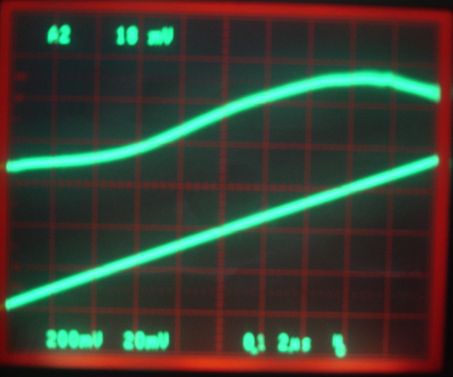
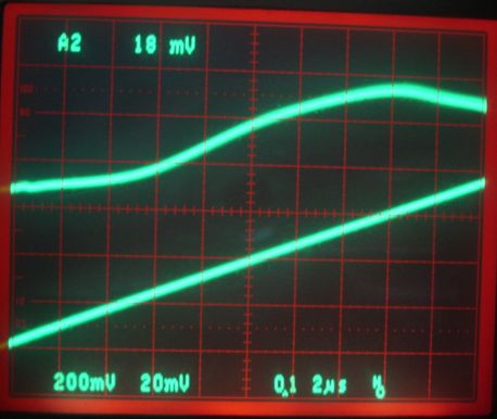
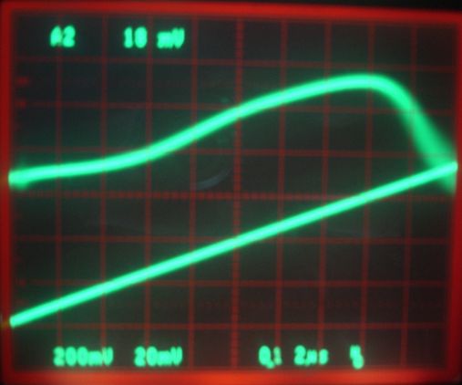
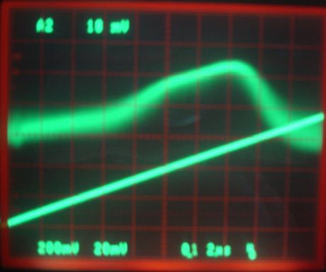
Figure: Demodulated Output versus Frequency for Various Input Powers. Top-left −4 dBm, top-right −34 dBm, bottom-left −64 dBm, bottom-right −76 dBm. In each display, the bottom trace is the TUNE input to our Modulating Transmitter (A3014MT) Serial Number 1 (for calibration of this circuit, see here. Each vertical division is 5 MHz, starting at 895 MHz on the far left, ending with 945 MHz on the far right. The top trace is the demodulator output.
Now we apply a square wave to the Modulating Transmitter's TUNE input. From the figure above, we see that a TUNE voltage of 1.1 V will produce a demodulated output of 1 V from the A3005B, and TUNE set to 1.3 V will produce and output of 3 V. So we drive the Modulating Transmitter with a 2-MHz square wave switching between these two voltages.
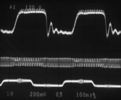 Figure: Reference Frequency Modulation. Upper trace is demodulated output, middle trace is limiting IF signal, sloping trace is the TUNE input to our Modulating Transmitter 70 cm away.
The center trace shows the IF frequency switching from 50 MHz (downshifted 970 MHz) up to 90 MHz (downshifted 930 MHz). The horizontal scale is 100 ns per division (as you can see by examining the oscilloscope screen itself). The demodulated output shows some bounce on the negative edges, but its response is fast, symmetric, and sharp. Its rise time is around 50 ns, which is half the rise time of the A3005A when operating with the A3006 transmitter.
Now we turn off the Modulating Transmitter, and turn on a Subcutaneous Transmitter (A3009). We program the A3009 to drive its own TUNE signal between 1.1 V and 1.3 V, just as we drive the VCO on our Modulating Transmitter. Both circuits use the MAX2624 VCO to generate their RF signal. With the help of the Programmer (A3011), we trigger our oscilloscope off the TUNE logic signal (not the actual TUNE voltage, but the logical sequence of 1's and 0's). This signal appears as the lower trace on the oscilloscope, in place of the Modulating Transmitter's TUNE input.

Figure: SCT Reception at Close Range (30 cm).
We hold the SCT 30 cm from the A3005B antenna, or even place the two flush up against one another, and then move it 2 m away. The signal we see on the oscilloscope changes very little. We see no reception dead spots as we move the transmitter around at ranges up to 2 m. The gain of the A3005B is sufficient to amplifier what is left of the signal in a dead spot, and produce a clear output. We could not move the transmitter farther from the receiver because both are connected to the oscilloscope with 1-m probes.
We turned on our Modulating Transmitter and placed it 70 cm from the A3005B. We set it to transmit at 950 MHz, right in the middle of our receiver pass band. We moved the A3009 towards and away from the receiver antenna. When the A3009 was within 50 cm of the antenna, its signal dominated that of the Modulating Transmitter, and we observed its signal on the screen. At farther ranges, the signal of the Modulating Transmitter garbled the SCT transmission, and then overwhelmed it. This is exactly what we were hoping for: to get a clear demodulated signal output so long as our SCT signal was stronger than the interference. Making sure the A3009 and A3005B work together in the presence of interference is a matter of making sure that the two are close enough together.
Signal Identification
Consider an A3005B Receiver at range r from an A3009 Transmitter. For any ambient interference, there exists a maximum range, rmax > 0, such that ∀ r < rmax, the receiver will obtain a clear signal from the transmitter. This was not true for the Receiver (A3005A) and Trasnsmitter (A3006) that we attempted to deliver to the Institute of Neurology in fulfillment of Stage Three of our Subcutaneous Transmitter development. In addition to the rmax constraint, the A3005A and A3006 combination was subject to a second constraint. The interference power had to be no more than 10 dB greater than the circuit's self-generated noise power. If the interference exceeded this +10dB threshold, the receiver would not obtain a clear signal from a transmitter at any range.
Although the A3005A and A3006 combination was so vulnerable to interference, its communication made signal identification easy. Compare the following receiver outputs.
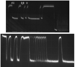
Figure: Top: A3005B reception of A3009 transmission. Bottom: A3005A reception of A3004 transmission.
The A3005A output is quiet when it is not receiving a signal from the transmitter. We can trigger an oscilloscope off a rising edge on the receiver output, and see the transmissions on the screen. But the A3005B output is not quiet when it is not receiving a signal. The A3005B gain is so great that its output is always swinging between its two extremes. Even with no interference, the A3005B amplifies its own internal noise until the demodulated output is a 2-V random signal. It is no longer possible for us to pick out the transmitter's signal in the receiver's output using a rising edge trigger. That's why we have to connect our oscilloscope to the TUNE logic output on the transmitter itself: it's the only way we can trigger our oscilloscope to show us how the transmission is received by the A3005B.
In the case of the A3005A with A3006, we were able to identify our transmitter signal by waiting for a rising edge on the A3005A output. In the case of the A3005B with A3009, we must watch for a sequence of transisions in the receiver output that is unique to the transmitter signal, therefore distinguishing it from interference and noise. Identifying this sequence of transitions will be the job of the Recorder (A3007B).
Because the noise output from the A3005B is random, and its interference-generated output might be random or pseudo-random, it is impossible to choose a sequence of transitions that will never occur in the absense of a genuine transmitter signal. The random nature of the noise and interference means that all sequences can occur. our signal identification requirement is not that we never record a false signal, but that we rarely recorde a false signal. We would like to waste no more than 10% of our Recorder (A3007B)'s memory with false signals, so we want to be 90% confident that an occurance of our identifying sequence of transitions corresponds to a genuine transmitter signal.
Conclusion
We consider the signal identification problem in more detail in our design of the Recorder, Version B (A3009B). For now, it appears that the A3005B meets our requirements, and we will proceed under the assumption that a dual receiver will not be required to ensure reliable data reception. The Stage Three reception system we hope will consist of one A3005B Receiver connected to one A3007B Recorder.