Command Transmitter-Receiver (A3023)
© 2012 Kevan Hashemi,
Open Source Instruments Inc.
Contents
Description
Design
Logic and Clock
Oscillator and RF Switches
Amplifier and Power Switch
Tuner and Demodulator
Power Threshold and Comparator
Transmission and Reception
Booster Amplifier
Faraday Enclosures
Conclusion
Description
The Command Transmitter-Receiver (A3023) is intended to test the command receiver we propose for the ISL (Implantable Sensor with Lamp) in our Conceptual Design. The A3023 is a LWDAQ Device in two parts. The Command Transmitter section contains a 146-MHz (2-m band) VCO, RF amplifier, and RF switches to provide 100% amplitude modulation. The Command Receiver section contains a tuner circuit, a demodulator, a comparator, and two indicator lamps.
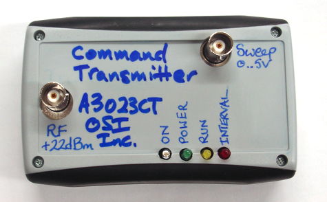
Figure: Command Transmitter (A3023CT) in Enclosure. ON is a blue lamp that indicates when the RF power is on. POWER is a green lamp indicated circuit power is connected. RUN is a yellow lamp that indicates a stimulus program is running. INTERVAL is a re lamp that flashes at the end of a stimulus interval.
The Command Transmitter (A3023CT) provides a BNC output for its RF power, and a LWDAQ device socket through which we can control the two RF switches and power to the RF amplifier. It provides a BNC input to modulate its VCO. By applying a 5-V triangle wave to the SWEEP input, the A3023CT will provide a near-linear sweep of 146±50 MHz. The A3023CT responds to LWDAQ commands with the same interface as the Lamp Controller A2060L, so that it's 146-MHz power output flashes on and off just as a lamp would flash on and off. The blue indicator lamp on the A3023CT flashes to indicate the RF power is on.

Figure: Command Transmitter (A3023CT) with Flexible Antenna. Here we see the A3023CT driving an antenna through a 2-dB attenuator, and stimulating an Implantable Lamp (A3024A). The 2-dB attenuator is necessary to stabilize the A3023CT power amplifier when driving a poorly-behaved load like an antenna. This arrangement supplies 100 mW (20 dBm) of 146 MHz RF power to the antenna, and is useful for testing Implantable Lamp circuits.
We use the A3023CT together with a booster amplifier to provide 1.6 W of RF power for reliable stimulation of implantable lamps at ranges up to 1 m.

Figure: Command Transmitter (A3023CT) with Booster Amplifier and Telescoping Antenna. Here we see the A3023CT driving a ZHL-3A+ booster amplifier through a 12-dB attenuator. The attenuator is necessary to avoid over-driving the input of the ZHL-3A+. The booster amplifier drives a half-wave telescoping antenna directly. This arrangement supplies 1.6 W (32 dBm) of 146 MHz RF power to the antenna, and is effective at stimulating Implantable Lamps at ranges 1 m (100% reliable) to 6 m (50% reliable).
The Command Receiver (A3023CR) provides two-pin connectors for RF input, 3-V power, and binary power detector output. We can solder a battery to the board directly if we like, in place of B1. The A3023CR is an experimental circuit designed to test the ISL crystal diode receiver design.

Figure: Command Receiver. Circuit power is supplied by a battery through the connector on the lower left. The RF command signal enters through the connector on the upper left. Two blue LEDs, one on the top and one on the bottom of the board, indicate when the power detector output is HI.
Here is a list of variations and accessories for the A3023. For stimulation of implantable lamps, we use the Command Transmitters (A3023CT), a 12-dB attenuator, a 30-cm coaxial cable, a booster amplifier, and a half-wave 146-MHz antenna.
| Part Number |
Description |
| A3023CTX |
Command transmitter with firmware P3023A01. |
| A3023CT |
Command transmitter with firmware P3023A02. |
| ZHL-3A+ |
Booster Amplifier. |
| HAT-12 |
12-dB coaxial attenuator. |
| Half-Wave 2-m |
Telescoping half-wave 146-MHz antenna. |
Table: A3023 Versios and Accessories.
You will find our experimental results in this spreadsheet (Open Office). The graphs we present below are made using the data in the spreadsheet.
Design
S3023_1: Command Transmitter
S3023_2: Command Receiver
A302301A.zip: PCB Gerber Files.
Firmware: Logic programs.
Command Reception: Conceptual design of the ISL command receiver.
Circuit Concept: Diagram of the comamnd receiver circuit in conceptual design.
PPL Enclosure: Drawing of the hand-sized plastic enclosure in which we mount the RF Amplifier.
ZHL-3A+: Booster amplifier to provide 1 W of antenna power.
CVCO33CL-0125-0200: Voltage-controlled radio-frequency oscillator used in the command transmitter.
Logic and Clock
[03-OCT-12] We adapt the A2075 firmware for the A3023. The LWDAQ Command receiver uses a ring oscillator to decode the serial commands arriving from the driver. The 32.768 kHz oscillator, U11, provides RCK for transmission timing. The logic chip provides 256 programmable logic gates for future applications. The P3023A01 firmware allows us to close switches X and Y individually with the LWDAQ command bits DC1 and DC2 respectively. Thus we can determine the isolation of each switch individually and together.
[14-DEC-12] The P3023A02 sets up the Command Transmitter as a Lamp Controller (A2060L). The pulse timing is driven by the A3023's 32.768-kHz clock instead of the 40-MHz clock used on the A2060L. Now we can control the A3023 with the Lamp Controller Tool. By setting the pulse time to 10 ms and the pulse interval to 20 ms, we create bursts of RF power 10 ms long at 50 bursts per second. If we activate the random interval machine (check the random box in the Lamp Controller Tool), we get pulses separated by a random time with average value 20 ms.
Oscillator and RF Switches
Here is the A3023CT circuit without the power amplifier.

Figure: Command Transmitter. This is the left-hand side of the A302301A circuit board. This particular circuit has all components loaded except for U8, which is bypassed by a 1-μF P1206 capacitor.
The oscillator is voltage-controlled with range 125-200 MHz. It is the source of our command radio-frequency carrier signal. We pass its output through two radio-frequency switches and an amplifier. These switches are the means by which we will modulate the carrier signal. Here we consider the operation of the switches without the amplifier.
[04-OCT-12] We assemble the Command Transmitter, omitting U8, the RF amplifier. We connect U8-1 to U8-3 with a capacitor. The output of the Command Transmitter is the output of the VCO, passed through two RF switches and a number of capacitors. The VCO is an CVCO33CL-0125-0200 from Crystek. The VCO is unstable with no decoupling capacitor on its tuning input. We add a 10 nF capacitor from U6-1 to 0 V, which is C22 in the schematic above. With 1.36 V on the tuning input, the output frequency is 146 MHz. There are two switches, X and Y, implemented by U7 and U9 respectively, each RF3024. Each can be open or closed. When open, the RF signal is terminated by 50 Ω (R6 and R7). We open and close the switches, and measure the power emerging at the RF output down a 1 m coaxial cable to a 50-Ω scope input.
| Configuration | RF Amplitude | RF Power
(dBm) |
|---|
| X closed, no amplifier, Y closed | 1.0 V p-p | +4.0 |
| X closed, no amplifier, Y open | 6.3 mV p-p | −40 |
| X open, no amplifier, Y closed | 5.0 mV p-p | −42 |
| X open, no amplifier, Y open | 0.8 mV p-p | −58 |
| board power disconnected | 0.3 mV p-p | −66 |
| X closed, no amplifier, Y closed, 10 MΩ probe on VCO output | 0.86 V p-p | +2.7 |
| X closed, amplifier, Y closed | 7.6 V p-p | +22 |
| X closed, amplifier, Y open | 7.6 V p-p | −17 |
| X open, amplifier, Y open | 1.0 mV p-p | −56 |
Table: Output Power for Switch and Amplifier Configurations.
Each RF switch appears to provide over 40 dB isolation at 146 MHz. The VCO is powered continuously. Its data sheet says its typical output power is +5.0 dBm. We see +4.0 dBm in this test, but with different loads on the RF output, we can see up to +6 dBm. We open and close both switches at 32.768 kHz, using RCK and observe the following development of RF power after the switches close.
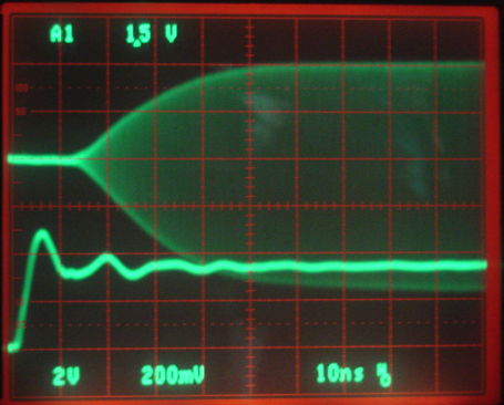
Figure: RF Switching of VCO Output. We are closing switches X and Y on the rising edge of the lower waveform. The upper waveform is the 146 MHz RF output.
The RF power turns on in around 50 ns. Although not shown in the figure above, the power turns off in the same 50 ns. Because our intended command transmission bit period is 30 μs, we see that our RF switches provide adequately fast response.
[15-JAN-13] We calibrate the VCO with the final version of our amplifier and power switches. We obtain the following relationship between frequency and TUNE input.

Figure: VCO Frequency versus TUNE Input. We obtain 146 MHz with 1.25 V at the TUNE input.
We use this calibration to translate TUNE into frequency when we sweep the TUNE input with a triangle wave.
[22-FEB-13] We connect each of our two A3023CT circuits to our oscilloscope and adjust VR1 until ten periods of its RF output equal 68.48 ns, for exactly 146.0 MHz. We do this with the 5-V power supply dropped to 4.68 V by the current drain of the A3023CT and various other LWDAQ devices. We disconnect these other devices and the 5-V power supply rises to 4.85 V. The RF output frequency rises to 146.8 MHz. When we disconnect the A3023CT, the power supply voltage rises to 4.92. There is a 0.23-Ω resistor in series with the 5-V supply and the A3023CT consumes 140 mA. We re-tune both A3023CTs so that their output frequency is 146.0 MHz when the 5-V supply is 4.85. Now, when the 5-V supply drops to 4.68 V, the frequency drops to 145.4 MHz.
[13-MAR-13] We measure the default frequency of our A3023CT and find it is 146.0 MHz.
Amplifier and Power Switch
The amplifier is U8. The power switch is Q1, shown below in the original version of the schematic. We have since removed Q1 and C9 from the board, for reasons given below. The idea was to turn on power to U8 by turning on Q1, which connects U8's ground pins to the local 0V. We would provide a high-frequency path to ground through capacitor C9.
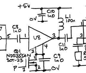
Figure: Power Switching for RF Amplifier. We connect its ground terminals with a MOSFET and a capacitor. But the amplifier oscillates when the switch is closed.
[04-OCT-12] We loaded U8, the MGA-31189 250 mW RF amplifier onto the board. We saw unstable bursts of power at the RF output. Something is wrong. Perhaps the power switch is causing problems. We may have RF power appearing on the gate of the power switch. The output of U8 looks as if the chip is powering up and then switching off in some kind of oscillation. We removed U8 and bypassed it with a 1 μF P1206 capacitor, leaving the amplification problem for another day.
[10-OCT-12] We remove Q1 and solder the U8 ground pad directly to our top ground plane. We increase L1 from the original 100 nH to 1 μH. The RF circuit now looks as shown below.
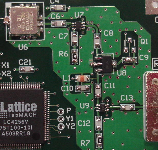
Figure: Command Transmitter's RF Amplifier Circuits. The top-side copper is mostly ground plane. The RF amplifier is U8, the RF switches are U7 and U9. The VCO is U6. Note the capacitor added to the U6 input, and the empty Q1 footprint.
With both switches closed, we now see on our RF output a 146-MHz signal with amplitude 7.9 Vp-p = 22 dBm. The output of the VCO is 1.0 Vp-p = 4 dBm. Thus U8 is providing 18 dB of gain.
[14-FEB-13] We build another A3023CT, this time with the BNC plugs and LEDs on the bottom side so we can better mount the circuit in a box for ION. We adjust VR1 until the VCO output frequency is 146.0 MHz. The TUNE input voltage is 1.30 V (compare to 1.25 V for previous circuit). We sweep the TUNE input of the VCO and connect the RF output to our oscilloscope with a coaxial cable and a 50-Ω termination. We obtain the following trace of peak-to-peak amplitude versus frequency.

Figure: Output Amplitude versus Frequency. The bottom trace is the TUNE input of the VCO, sweeping from 0 V to 4 V. The frequency increases from 120 MHz to 200 MHz. To trace is the RF output. Its vertical spread is the peak-to-peak amplitude. At 146 MHz we have 8.65 V p-p.
At 146 MHz, the amplifier produces 8.65 V p-p into 50 Ω, which is 190 mW or 23 dBm.
[12-FEB-14] With a 12-dB attenuator in series with the A3023CT RF output, and a 146-MHz whip antenna, we are transmitting roughly 11 dBm. At range of 50 cm, this 10 dBm disturbs the electrical current measurement of both our 24-V bench power supplies. We move the antenna to range 1 m and insert a 30-dB attenuator to stop the effect. This observation alerts us to the possibility of sustained 146-MHz RF power disturbing other third-party electronic circuits.
Tuner and Demodulator
The Command Receiver tranforms the RF signal it picks up with its antenna into a logic output. To do this, it uses a tuner, a demodulator, and a comparator. We also have two blue LEDs to show us when the comparator output is HI, which indicates RF power above a threshold.
The tuner consists of resistor R8 and the tank circuit L2 in parallel with VC1, C14, and C15. In the prototype, we load VC1 with a 4-25 pF variable capacitor and omit C14 and C15. We choose R8 = 1.0 kΩ so that it's resistance is small compared to the video resistance of our detector diode, RV ≈ 8 kΩ. We choose L2 = 100 nH so that its impedance at 146 MHz is low compared to R8, and its self-resonant frequency is well above 146 MHz. We use the AISC-0805-R10J. We also have C20 = 10 pF, a coupling capacitor whose impedance is much less than R8. The following plot shows the calculated gain of the tuner with frequency for three values of VC1.

Figure: Calculated Gain of Tuning Circuit. We use R8 = 1 kΩ, RV = 8 kΩ, L2 = 100 nH, and three values of VC1. The gain is the ratio fo the amplitude VT to the amplitude of the RF input on C20 and R8.
The demodulator consists of a HSMS-285C dual, zero-bias, schottky detector diode with dynamic resistance of 8 kΩ. We can connect one or both of these diodes to the tuner output. By default, we will omit R9 so as to connect only one of the diodes. The far side of the detector diode is connected to capacitor C16. The demodulated signal develops across this capacitor. Our original schematic called for C16 = 2.7 nF, but subsequently we changed this to 270 pF.
[05-OCT-12] We start by testing the tank circuit and detector diode at a frequency we can produce with our function generator and observe more reliably with our oscilloscope probes. We let C20 = 1.0 μF, L2 = 1.0 μH, and C14 = 400 pF. We omit VC1, C15, and R9, and we leave R8 at 1.0 kΩ. The resonant frequency of L2 and C14 should be 8 MHz. The following figure shows the amplitude of VT as we sweep the the RF frequency.
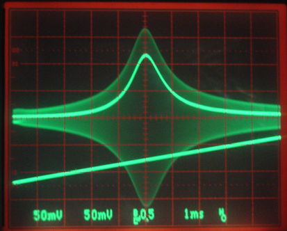
Figure: Resonance of 8-MHz Tank Circuit. The fuzzy trace is VT, the RF signal on the tank circuit. The solid signal is VR, the signal at the output of the detector diode. The input RF amplitude is constant while the frequency increases from 3 MHz to 12 MHz. The display is bandwidth-limited to 20 MHz by the oscilloscope.
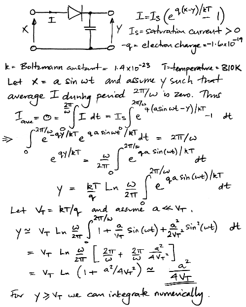
The figure also shows VR, the voltage across C16, as the amplitude at VT changes. In this experiment we have C16 = 2.7 nF. We discuss the behavior of this diode, and how it can detect RF power in our Conceptual Design. The diode cooperates with capacitor C16 to produce a DC voltage that increases with the amplitude of VT. Here we see the diode producing a peak that it produces a DC voltage of 114 mV for an input amplitude of 170 mV.
Leaving the input frequency fixed at 8 MHz, we measured VR as a function of VT. The following graph shows our measurements along with the theoretical response we obtained by numerical integration and calculation. We see superb agreement between measurement and calculation at 8 MHz.

Figure: Detector Output versus Input Amplitude. The input amplitude is half the peak-to-peak amplitude. Measurements obtained at 8 MHz and 19°C. Calculations obtained for 37°C and numerical integration. The calculated graph does not vary significantly for 0°C to 60°C.
[09-OCT-12] We assemble another tuner, this time with the component values called for in our schematic, except we use 2.7 nF for C16. We load VC1, a 4-25 pF variable capacitor, but not C14 or C15. We omit R9 so as to use only one detector diode. We have C20 at 10 pF to allow 146 MHz into the tuning circuit. The impedance of 10 pF at 146 MHz is only 110 Ω, which is small compared to R8 of 1 kΩ. We apply +4 dBm at 146-MHz to the RF input connector, P2, with the help of a BNC to two-pin adaptor. We measure VR and adjust VC1 until we get the maximum DC voltage from the diode. We cannot measure VT directly with a 10-MΩ oscilliscope probe because we find that its 1.5-pF capacitance disturbs the tuning. Thus we tune the tank circuit without a probe attached. At the resonant frequency, we trust that the gain of the circuit is close to 0.9.
[11-OCT-12] In the HSMS-285C data sheet, we see a demodulator circuit that uses two diodes arranged as the diodes of U10 are arranged in our circuit, were we load a 0-Ω resistor for R9. We did not understand how the second diode could improve the gain of the demodulation. But we resolved to include the second diode in our circuit so we could try it out. We apply 60 mV of 146 MHz to our demodulator and we get 20 mV on VR. We apply a lump of solder to R9 so as to introduce the second diode. We get 18 mV on VR. This drop is what we expect, because the second diode loads the filter circuit so as to decrease the filter output amplitude. We conclude that we cannot benefit from a second diode.
[11-OCT-12] Our tuning inductor has 5% tolerance. Its self-resonant frequency is >1.2 GHz, which implies that its parallel parasitic capacitance is less than 0.2 pF. For resonance at 146 MHz, we need a total of 11 pF in parallel with our 100 nH. The HSMS-285C diode has capacitance 0.3 pF. We remove VC1 and increase C14 from 0 pF to 20 pF by adding 1-pF capacitors. For each value of C14, we measure the frequency at which VR is greatest. We apply our RF power through a BNC cable and a 36 dB attenuator.
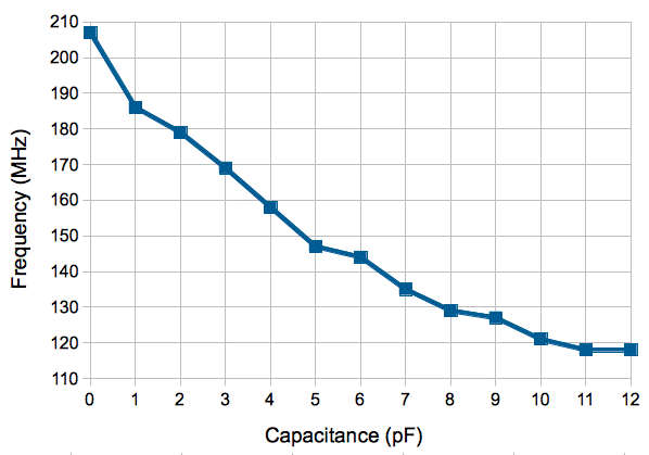
Figure: Frequency of Peak Demodulated Output versus Tuning Capacitance.
The VCO range is 118 MHz to 207 MHz, so we cannot find a resonant frequency outside this range. The VCO output amplitude varies slowly with frequency, so that the amplitude of the RF input to our tuner decreases from 60 mV at 118 MHz to 40 mV at 207 MHz. The 1-pF capacitors we use have tolerance ±0.25 pF. It is possible that the value of C14 with 10 of these capacitors is as low as 7.5 pF or as high as 12.5 pF. But when we made 5 pF out of two 10-pF capacitors in series, we obtained a peak frequency of 152 MHz, very close to the 147 MHz we obtained with the five 1-pF capacitors. Despite our sources of error, it remains significant that our tuner resonates at 146 MHz with only 5 pF, when our expectation was 11 pF.
[12-OCT-12] We wonder if our L2 might be 220 nH instead of 100 nH. We replace it with a 100-nH inductor from another component bag, purchased several years ago. The peak frequency is now 149 MHz. We conclude that both inductors are close to 100 nH.
[11-OCT-12] We load 5 fresh 1-pF capacitors into our C14 and C15 footprints. We apply a triangle wave to the TUNE input of our Command Transmitter. We connect the RF output of the transmitter to the RF input of the receiver through a series of attenuators (we did not record the attenuition). We obtain the following plot of VR versus TUNE. The peak frequency is 148 MHz.

Figure: Resonance of 148-MHz Tank Circuit. The top trace is the TUNE input to the VCO, which rises from 0 V to 2.5 V, during which the frequency increases from 118 MHz to 175 MHz. The bottom trace is VR.
The figure above shows VR as a function of frequency, with the left edge at 118 MHz and the right edge at 176 MHz. The peak occurs at 148 MHz. The VCO is almost linear in the region displayed (if we assume 5.7 MHz/div we get the peak at 151 MHz). At a frequency 20% above the peak frequency, the demodulated output is 10% peak value.
[11-OCT-12] The Command Receiver should not respond to the 910-MHz data transmissions of the ISL, which are going to be identical to those of the SCT. We take out our 910-MHz SAW Oscillator A3014SO, which provides +13 dBm output power. We apply this with attenuators to the RF input of our Command Receiver and measure VR, the demodulated output. We obtain the following graph.
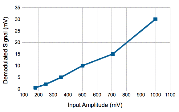
Figure: Response of Tuner and Demodulator to 910 MHz (Data Frequency) Power. We give the DC demodulator voltage versus the amplitude of the incoming 910 MHz, as deduced from our knowledge of its power feeding a 50-Ω terminator.
We expect to place our power threshold at around 10 mV, so that when VR is greater than 10 mV, the Command Receiver detects a bit-value of one. In order for 910 MHz to produce a false one-bit, we must apply a 500-mV amplitude to its tune input. The 910-MHz signal generated by an SCT is −3 dBm, which has an amplitude of 150 mV. Even if the entire 910 MHz amplitude is somehow transferred from the ISL's data antenna to its command antenna, this power will still be insufficient to create a false one-bit.
[28-JAN-13] After an hour of loading various capacitors and resistors into the tuner circuit, we conclude that the layout of our components, with the use of a thin track over a ground plane, interferes with the operation of small capacitors. We have not performed a calculation and tested this hypothesis, but we are convinced enough to abandon further work on the tuner circuit in the A3023CR. We find that the A302401A layout provides resonance at the expected values of components, so we continue our work on that board instead, see M3024.
Power Threshold and Comparator
Comparator U12 in the Command Receiver compares VR to a threshold. The comparator is a MCP6541. It has typical input offset voltage ±1.5 mV and input hysteresis 3.3 mV. We set the threshold by adjusting VR2 until the U8 output went high for an 8-mV voltage on VR. Indicator lamps LED5 and LED6 show us when the comparator output goes HI. We take our +4 dBm, 146-MHz signal, pass it through a 24-dB attenuator and apply it to the RF input of the receiver. We terminate the attenuators with the 50-Ω input of our oscilloscope. The following figure shows the RF input, the diode output, and the comparator's output.
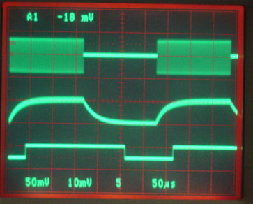
Figure: Power Detection with 40-mV 146-MHz Input. We have C16 = 2.7 nF. The top trace is the RF input, 50 mV/div. Center trace is the diode output, VR, 10 mV/div. The bottom trace is the output of the comparator. The time scale is 50 μs/div.
The amplitude of the input RF is 40 mV (half the peak-to-peak voltage). At the resonant frequency of our tank circuit, we hope the gain of the tuner is close to 0.9, in which case the amplitude of VT will be around 35 mV. Looking at our diode response, we expect VR for a 35-mV input to be around 10 mV. The figure above shows VR reaching a value just above 10 mV. Thus we conclude that our tuning circuit and diode are functioning as well as they did when we tested them at 8 MHz.
The comparator output goes high when VR gets above 8 mV, and falls when VR drops below 2 mV. This suggests the hysteresis of the comparator is 6 mv. The maximum hysteresis specified in the data sheet is 6.5 mV. We see that the hysteresis delays the turn-off more than the turn-on, and so diminishes the length of the LO part of the comparator output. As we increase the RF amplitude, this problem becomes more severe, until the comparator ourput remains HI all the time. The following figure shows the same traces, but for an input of 600 mV.
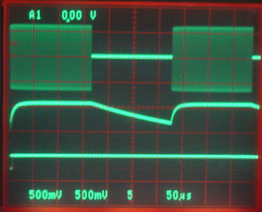
Figure: Power Detection with 600-mV 146-MHz Input. We have C16 = 2.7 nF. The top trace is the RF input, 500 mV/div. Center trace is the diode output, VR, 500 mV/div. The bottom trace is the output of the comparator. The time scale is 50 μs/div.
Here we see another problem appearing: the time constant of VR is of order 10 μs when the RF turns on, and 100 μs when the RF turns off. The impedance of the detector diode, RV is small when it is forward-biased and large when it is reverse-biased. Indeed, with 600 mV of reverse biase, the current flowing in the reverse direction is equal to the diode's leakage current. According to the HSMS-285C data sheet, its maximum reverse leakage current is 175 μA. We see C16 being drained by a current of around 7 μA.
We load 270 pF into C16, replacing the original 2.7 nF called for by our design. We repeat the above experiment and obtain the following signals. We see the discharge takes only 30 μs, and still looks like a linear discharge rather than an RC relaxation. We see that our comparator output goes HI within 4 μs of the RF power start, and LO within 80 μs of the stop, for a total skew of around 80 μs.
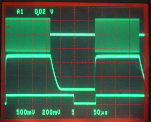
Figure: Power Detection with 600-mV 146-MHz Input. We have C16 = 270 pF. The top trace is the RF input, 500 mV/div. Center trace is the diode output, VR, 200 mV/div. The bottom trace is the output of the comparator. The time scale is 50 μs/div.
We reduce the incoming RF amplitude to 40 mV. The same threshold still works well. The comparator output goes HI within 20 μs of the RF power start, and LO within 60 μs of the stop, for a skew of 40 μs.

Figure: Power Detection with 60-mV 146-MHz Input. We have C16 = 270 pF. The top trace is the RF input, 50 mV/div. Center trace is the diode output, VR, 5 mV/div. The bottom trace is the output of the comparator. The time scale is 50 μs/div.
We want to use the demodulated signal to receive a serial data at 8 kBits/s, which means each bit will take 125 μs. For this, we would like the timing skew introduced by the power threshold to be less than 40 μs for inputs 40 mV to 600 mV. We play around with the threshold until we have a timing skew at 40 mV of 23 μs − 42 μs = −19 μs and at 600 mV we have 59 - 4 = 55 μs. Perhaps this will be good enough. If not, we could take steps to limit the value of VR so as to avoid over-charging C16.
[11-OCT-12] We disconnect the Command Receiver's indicator lamps and measure its current consumption without them. When there is no incoming RF power, the circuit consumes 0.4 μA. With RF power switching at 3 kHz continuously, current consumption rises to 4.2 μA. We remove C19, the filtering capacitor on the output of the comparator. Current consumption at 3 kHz drops to 0.6 μA. If the disconnect power, we still see our demodulated signal on C16 because the power for the demodulation comes from the RF signal itself. We conclude that our command receiver can provide 8 kbit/s reception for around 1 μA.
Transmission and Reception
[10-OCT-12] We connect a stiff, bent, 15-cm wire to the RF input of our Command Receiver. We connect a EXB-136-BNX rubber duck antenna to the RF output of our Command Transmitter. The detector lamps turn on when we hold the receiver 10 cm from the antenna.
We soon discover that our power amplifier does not perform well with the rubber duck antenna as a load. The rubber duck antenna is tuned to have 50-Ω input impedance in the range 136-144 MHz. We are operating at 146 MHz. The power amplifier output becomes distorted and drops to around 16 dBm. We add a 3-dB attenuator between the amplifier and the antenna. Amplifier output power rises to 22 dBm again, and we now see 19 dBm at the antenna input. We have noted the stabilizing effect of attenuators in our design of our A3015A antenna.
As we rotate the receiver, we watch the blue indicator lights driven by the comparator output. We see the lights go out when we hold the antenna perpendicular to the transmitting antenna. We have studied this problem of orientation at length for the reception of our subcutaneous transmitter 915 MHz signals, as we describe in Omnidirectional Antennas. We remove the rubber-duck antenna and try in its place a variety of wire antennas, including a 2-m full-wave loop, a 50-cm quarter-wave whip, and a 50-cm open-ended loop (the wavelength of 146 MHz is close to 2 m). We obtain the most reliable reception with the 50-cm open-ended loop with 3-dB attenuator at its base. The following figure shows the demodulated signal in the receiver with the two antennas separated by 110 cm. At this range, the two antennas must be oriented favorably.
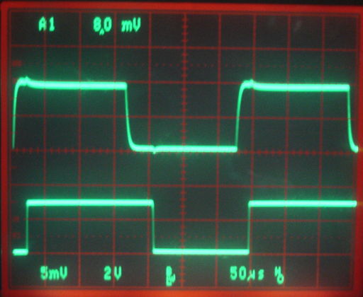
Figure: Radio Reception At 110 cm. We have a stiff 15-cm wire for the receiving antenna and a 3-db attenuator with 50-cm loop of wire for the transmitting antenna. The top trace is the detector diode output, 5 mV/div, and the bottom trace is the comparator output, 2 V/div. To remove traces of 146-MHz, both traces are bandwith-limited to 20 MHz.
We try placing the transmitter on a metal ground plane to see if this will improve reception. We can discern no improvement. We place the transmitter on an insulating surface. We see no change.
[11-OCT-12] With the transmitter sitting on a metal desk with an insulating veneer, we take the receiver in our hand and move and rotate it around the transmitting antenna. We can see when reception fails because the blue LEDs on the top and bottom of the circuit board turn off. At range 20 cm from the antenna center, failure occured for 0 s out of 60 s, at 30 cm for 2 s out of 60 s, at 50 cm for 6 s out of 60 s. Using our definition of reception robustness, we have robustness 100%, 97%, and 90% at ranges 20 cm, 30 cm, and 50 cm respectively.
In our Conceptual Design we estimated that 30 dBm would be required for us to obtain reliable reception at 50 cm. Our bent transmitting antenna receives 19 dBm from the Command Transmitter (22 dBm output from amplifier with 3 db attenuator). This 19 dBm is adequate for reliable reception at 20 cm. With 30 dBm, or 12 times as much power, we can hope for reliable reception at √12 × 20 cm = 70 cm.
[14-DEC-12] With the Booster Amplifier added to the Command Transmitter (see below), we tried various combinations of transmitting and receiving antennas. The best receiving antenna was the quarter-wave coil and whip, which we made out of 50 cm of insulated wire coiled for most of its length, but with 10 cm straight. This simple antenna is not practical for implantation, so we experimented with stretched and un-stretched steel springs, both 150-mm long, as they would be for a rat implantation. The unstretched spring worked better. It contains roughly 50 cm of steel wire coiled into a spring. The rubber duck antenna performed slightly better, in qualitative tests, than the quarter-wave loop antenna. This contrasts with the superior performance of the quarter-wave loop without the booster amplifier.
We connected the rubber duck antenna and the un-stretched spring. We set the command transmitter to emit 5-ms pulses at 100 Hz. We held placed the antenna on a desk top as shown above, and moved the command receiver at random at range 100 cm and observed 2 s of reception failure in 60 s. Thus we have 97% robustness at 100 cm.
[19-DEC-12] We disconnect the battery with twisted pair power leads from P3 on the Command Receiver. We load a BR1225 battery onto the Command Receiver instead. Reception improves immediately with all combinations of antennas. We take a 200-mm piece of silicone-coated stranded steel wire and form it into a coil with two turns, as shown below.

Figure: Small Loop Antenna.
We use this small loop as a receiving antenna. One end is connected to the Command Receiver's RF input (P2-1) and the other end to the RF ground (P2-1). Thus it is a terminated loop antenna. We connect the booster amplifier, and use for a transmitting antenna a 2-dB attenuator and our quarter-wave unterminated loop (item 7 here). We attach the Command Receiver to the and of a stick and rotate and move it at random at range 1 m and see 0 s of signal loss in 60 s. At range 2 m, we see 2 s of signal loss in 60 s. At 3 m we see 4.3 s of loss in 60 s. Thus we appear to have robustness 100%, 97%, and 93% for ranges 1 m, 2 m, and 3 m respectively. We try the rubber duck antenna transmitting antenna and obtain similar results.
[20-DEC-12] We receive from Smiley Antenna a selection of 146.25 MHz (2-m wavelength) antennas. We show these, together with our original 140-MHz rubber duck and our quarter-wave loop.

Figure: Selection of Transmitting Antennas. (1) Quarter-wave unterminated loop with 2-dB base attenuator, 24 cm high. (2) 146-MHz 1/2-Wave Telescopic Antenna, 91 cm high when fully extended, 22 cm when collapsed, Smiley Antenna. (3) 146-MHz 5/8 Slim Duck, 30 cm high, Smiley Antenna. (4) 146-MHz Slim Duck, 22 cm high, Smiley Antenna. (5) 140-MHz Rubber Duck, 18 cm high, Laird EXB-136-BNX. (6) 146-MHz Mini Duck, 11 cm high, Smiley Antenna.
We perform the following experiment to compare the performance of these antennas in conjunction with our small loop Command Receiver antenna. We move away from the Command Transmitter, rotating and translating the Command Receiver on the end of a stick. We record the range at which robustness drops to 50%. We do this with and without the Booster Amplifier. We stabilize our power amplifier and booster amplifier with a 2-dB attenuator at the base of each antenna. The unterminated loop antenna already has a stabilizing attenuator. We do not add a second attenuator.
| Antenna | Range 30 dBm
(cm) | Range 20 dBm
(cm) |
|---|
| 1/4 Wave Unterminated Loop, Home-Made | 500 | 120 |
| 1/2 Wave Telescopic, Smiley Antenna | 600 | 200 |
| 5/8 Wave Slim Duck, Smiley Antenna | 480 | 180 |
| 1/4 Wave Slim Duck, Smiley Antenna | 450 | 120 |
| 1/4 Wave Rubber Duck, Lairde Technology | 470 | 180 |
| 1/4 Wave Mini Duck, Smiley Antenna | 460 | 120 |
Table: Effective Range of Various Transmitting Antennas. We have two sources of power. One is 20 dBm from our Command Transmitter amplifier, after a 2-dB stabilizing attenuator. The other is 30 dBm from our Booster Amplifier, after a 2-dB sabilizing antenna.
Although our measurements are crude, and are no doubt corrupted by the metal shelves and cabinets in our laboratory, we see that the half-wave telescoping antenna performs better than the others. We connect this antenna to our Command Transmitter's amplifier without a stabilizing attenuator. We obtain range 250 cm for 50% robustness. We connect it directly to the output of our Booster Amplifier and obtain a range of 630 cm. We conclude that the half-wave antenna is not only the most efficient radiator of power fed into its base, but is also a better-behaved load than the tuned rubber duck antennas.
We connect the half-wave telescoping antenna directly to the Booster Amplifier and rotate the Command Receiver randomly at range 3 m. We see 5 s of signal loss in 60 s. At range 2 m we see 0 s of loss. We have robustness 100% and 92% at ranges 2 m and 3 m respectively.
With the half-wave telescoping antenna connected directly to the Booster Amplifier, we try a 5-turn, 3-cm diameter loop antenna on the Command Receiver. We use insulated, 22-gauge, stranded, tinned copper wire. We obtain 50% robustness at range 150 cm. When we switch back to our 2-turn, 3-cm diameter loop made out of stranded stainless steel we once again obtain 50% robustness at 630 cm. We break the connection between the 2-turn loop and the Command Receiver RF ground, so as to make an unterminated loop antenna. We obtain 50% robustness at 300 cm.
Booster Amplifier
[14-DEC-12] We connect our Command Transmitter's 22-dBm output through a 12-dB attenuator to a ZHL-3A+ booster amplifier, and thereafter to our antenna.

Figure: A3023C, Command Transmitter with Booster Amplifier. (1) A3023B, (2) ZHL-3A+, (3) Rubber duck 146-MHz quarter-wave antenna, (4) Unstretched steel spring receiving antenna, (5) Stretched steel spring receiving antenna, (6) 24-V power for booster amplifuer, (7) Quarter-wave loop transmitting antenna with base 2-dB attenuator, (8) Quarter-wave coil and whip receiving antenna, (9) A3023CR.
The 12-dB attenuator keeps the power applied to the booster amplifier down to 10 dBm, which is the recommended maximum. If we connect the booster amplifier output to our oscilloscope, we observe 31.6 dBm (24-V p-p). In the photograph above, we see the rubber duck antenna connected directly to the booster amplifier. We assume it receives the full 31.6 dBm (1.4 W) of RF power.
Faraday Enclosures
[12-OCT-12] Within a faraday enclosure, reflections create reception dead spots. We have not yet tested our Command Transmitter and Receiver in a 70-cm faraday enclosure such as the ones in use with the current SCT systems. The absorbers we use in these faraday enclosures to dampen reflections at the 910-MHz data frequency do not work well at our 146-MHz command frequency. Thus we are prepared to encounter reception problems within our faraday enclosures. We will start our experiments soon.
[14-DEC-12] We cannot get our 146-MHz antenna to operate properly in a 70-cm faraday enclosure. It may be that shorter, tuned, vertically-polarised antennas would give better results. But we have decided to build a canopy enclosure with an absorbant mat on the floor, and we will test our command reception in such an enclosure.
Conclusion
[21-DEC-12] The Command Transmitter (A3023CT) and Booster Amplifier (ZHL-3A+) together produce and modulate 1.4 W of 146-MHz radio-frequency power. We transmit this power with a 91-cm long, commercially-made, half-wave antenna. On the Command Receiver (A3023CR) we provide power with a BR1225 battery and use a home-made, 2-turn, 3-cm diameter, loop antenna of stranded steel wire. We transmit 5-ms bursts of RF power at 100 Hz. At range 2 m, we see no loss of reception in any orientation. At range 3 m, we see loss of reception in 8% of orientations.
The Command Receiver consumes less than 1 μA quiescent current if we remove its indicator lamps. It is so effective at rejecting 910-MHz interference that even a subcutaneous transmitter antenna connected directly to its RF input will not cause it to generate an erronious one-bit.
The Command Receiver presents one of the biggest technical challenges we describe in the ISL Conceptual Design. Our greatest concerns were the reliability of command reception at ranges up to 50 cm, rejection of data frequency power, and its current consumption while receiving 8 kbits/s. With these prototype circuits, we achieve better than 99% reliable reception at range 200 cm. At ranges less than 100 cm, we are confident that reception will be 100% reliable.
We will test reception in our first canopy enclosure when it is available. We suspect that we will have to accept that reception cannot be 100% reliable throughout the enclosure, but we can hope for reliable within 100 cm of the transmitting antenna.