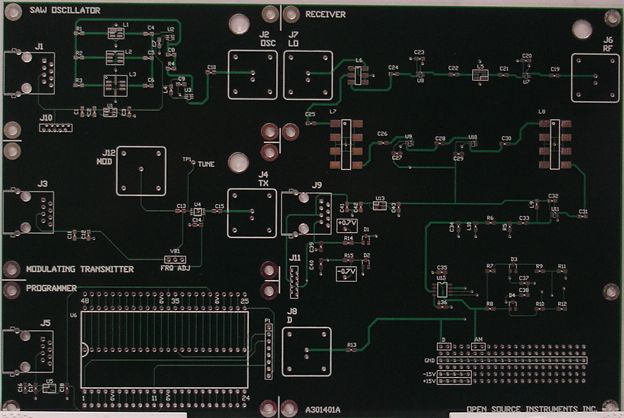
Figure: The A301401A Printed Circuit Board.
The RF Tester (A3014) is a combination of four circuits. Its purpose is to test several circuit ideas, both by implementing them, and by providing better support circuits for their development.
The four circuits are listed below.
| Version | Description |
|---|---|
| A3014DR | Demodulating Receiver |
| A3014SO | SAW Oscillator |
| A3014TP | TQFP-48 Programmer |
| A3014MT | Modulating Transmitter |
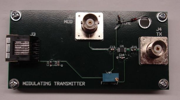
The Modulating Transmitter (A3014MT) replaces our original Modulating Transmitter (A3001A). The A3014MT allows you to set the DC voltage applied to a MAX2624 with a potentiometer, and then AC couple your modulation waveform through a BNC socket.
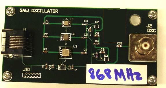
The SAW Oscillator (A3014SO) uses precise SAW filters to produce precise RF reference frequencies. We can use these as stable, accurate local oscillators for downshifting our RF signals, or we can use them as reference RF signals with which to calibrate our receivers.
The TQFP-48 Programmer (A3014TP) uses a TQFP-48 socket to program Lattice Semiconductor LC4064 chips in 48-pin thin quad flat pack packages. This allows us to program the chips before mounting them on a transmitter, so that no programming connection need be present on the transmitter.
The Demodulating Receiver (A3014DR) takes as input an LO and RF signal through BNC sockets. The LO should be +7 dBm for optimal operation of the A3014DR's mixer. The RF signal should be in the 900-MHz ISM band. The A3014DR output is the demodulated RF signal, similar to that of the A3005B.
S3014_1: SAW Oscillator (A3014SO).
S3014_2: TQFP-48 Programmer (A3014TP) and Modulating Transmitter (A3014MT).
S3014_3: Demodulating Receiver (A3014DR), RF amplifier, SAW filter, mixer, IF amplifier, discriminator, demodulator.
S3014_4: Demodulating Receiver (A3014DR), power supplies and board layout.
Warning: The A3014SO is not stable when connected directly to an antenna. Use a 6-dB attenuator between the output and the antenna base.
This circuit uses the phase shift and attenuation of SAW filters to create a SAW oscillator. The circuit gives us a choice of three different SAW filter footprints to choose from. We select which footprint to use by means of R1-R3 and C4-C6. The footprints L1, L2, and L3 are for 3.0-mm, 3.8-mm, and 5.0-mm surface mount packages respectively.
| Part | Nominal Pass Band (MHz) | Package |
|---|---|---|
| AFS869S3 | 865.0-873.0 | 3.8-mm |
| AFS915S3 | 911.5-918.5 | 3.8-mm |
| AFS916.5S3 | 913.0-920.0 | 3.8-mm |
| B3563 | 862.5-865.5 | 3.0-mm |
| B3570 | 867.4-869.4 | 5.0-mm |
| B3574 | 867.3-869.3 | 5.0-mm |
| B3588 | 902.0-928.0 | 3.0-mm |
The 5.0-mm footprint on the A3014SO is incorrect. It uses pins 2 and 6 for the input and output respectively, instead of pins 1 and 5. The SAW filters in position L3 sometimes work but not always.
With C2 and C3 both 1 μF, we found that U2 and U3 would blow occasionally when we plugged power into the circuit. We increased C2 and C3 to 10 μF. After that, U2 and U3 survived one hundred power connections on both the SAW Oscillators we used in our experiments.
The coupling we use to connect the SAW filter to its oscillation amplifier (U2 in the schematic) affects the frequency and stability of the oscillator. No matter what coupling we use, it is always possible, by touching and handling the circuit, to stop oscillations in the SAW filter pass-band, and provoke a parasitic oscillation outside the SAW filter pass-band. These oscillations may have one of two causes. The UPS2764 is stable only for near-50Ω loads, and the SAW filters do not act like 50-Ω loads outside their pass band. The amplifier may be transmitting its output to its input by means of the long tracks on the circuit board. If we want to suppress such transmission, we must lay out the board more carefully, with coplanar wave guides, as in the A3021B. In any case, we call these oscillations, outside the SAW filter pass-band, parasitic oscillations.
The following table shows the effect of various components for R2 and C5 when we used them to connect an AFS869S3 in a 3.8-mm package from Abracon. The filter's pass-band is 869±4 MHz. In each case, we describe how easy it is to provoke parasitic oscillations.
| R2 | C5 | Parasitic Oscillations |
|---|---|---|
| 51 Ω | 100 pF | Start when touching U2, persists thereafter. |
| 100 pF | 100 pF | Start when touching U2, stop thereafter. |
| 0 Ω | 0 Ω | Can start or stop when touching U2. |
| 10 pF | 10 pF | Can start or stop when touching U2. |
| 51 Ω | 51 Ω | Always (never SAW pass-band oscillations). |
| 1 nF | 1 nF | Can start or stop when touching U2. |
| 10 nH | 10 nH | Never (always SAW pass-band oscillations). |
The AFS869S3 is stable with inductive coupling. The same is not true for other SAW filters. Some are more stable with inductive coupling than with capacitive, others are less stable. In all cases, the oscillator sometimes powers up into parasitic oscillations. We frequently have to unplug the power and then plug it in again in order to get the oscillators in our experiments to work. When we connect the A3014SO to the LO input of our Demodulating Receiver (A3014DR), the connection can provoke parasitic oscillations in U3. The fuzzy signal on some IF waveforms is the downshifted version of a parasitic oscillation.
| A1 (dB) | A2 (dB) | Cable (cm) | IF |
|---|---|---|---|
| 0 | 3 | 30 | non-sinusoidal |
| 0 | 12 | 30 | sinusoidal |
| 0 | 3 | 90 | non-sinusoidal, fuzzy |
| 0 | 12 | 90 | non-sinusoidal, fuzzy |
| 3 | 3 | 90 | non-sinusoidal |
| 6 | 3 | 90 | sinusoidal |
We set up two A3014SO's, one with an AFS869S3, the other with an AFS915S3. One oscillates at 868 MHz and the other at 910 MHz. We measure their output power with our ZAD-11 mixer, as described elsewhere, and observe +13 dBm for both oscillators.
We attenuate one by 12 dB for the RF input of a mixer, and the other by 6 dB for the LO input. The following table gives the IF frequency we obtained from mixing the output of our two A3014SOs, for various types of coupling. In each case, we give the values of R2 and C5 for each circuit.
| AFS869S3 R2, C5 | AFS915S3 R2, C5 | Intermediate Frequency (MHz) |
|---|---|---|
| 10 nH, 10 nH | 10 nH, 10 nH | 30 |
| 10 nH, 10 nH | 100 pF, 100 pF | 38 |
| 100 pF, 100 pF | 100 pF, 100 pF | 47 |
| 100 pF, 100 pF | 10 nH, 10 nH | 36 |
| 51 Ω, 100 pF | 10 nH, 10 nH | 37 |
| 15 nH, 15 nH | 10 nH, 10 nH | 30 |
| 15 nH, 100 pF | 10 nH, 10 nH | 37 |
| 0 Ω, 100 pF | 10 nH, 10 nH | 27 |
| 100 pF, 10 nH | 10 nH, 10 nH | 37 |
| 0 Ω, 0 Ω | 10 nH, 10 nH | 37 |
The impedance of a 100 pF capacitor at 1 GHz is less than 2 Ω. When compared to the 50-Ω input and output impedances of the SAW filters, these capacitors are like short circuits. The phase shift they introduce is the same as the phase shift introduced by a resistor. The impedance of a 10-nH inductor, on the other hand, is 60 Ω at 1 GHz. When driving a 50-Ω resistor at 1 GHz, 10 nH introduces a phase shift of −51° and 15 nH introduces a phase shift of −62°.
The phase shift of the coupling network affects the oscillation frequency in a manner that depends upon the filter. The inductively-coupled frequency of the AFS869S3 is 8 MHz higher than its resistively-coupled frequency. The inductively-coupled frequency of the AFS915S3 is 10 MHz lower than its resistively-coupled frequency.
We tried three new filters, the B3570 868.4±1 MHz 5.0-mm, B3574 868.3±1 MHz 5.0-mm, and B3563 864.0±5 MHz 3.0-mm. We mixed the outputs of two A3014SO's, each with their own SAW filter and looked at the intermediate frequency. The following table shows what happened when we used inductive and capacitive coupling for each filter.
| LO SAW, Coupling | RF SAW, Coupling | Intermediate Frequency (MHz) |
|---|---|---|
| AFS869S3, 100 pF | AFS915S3, 10 nH | 36 |
| B3570, 100 pF | AFS915S3, 10 nH | 32 |
| B3570, 10 nH | AFS915S3, 10 nH | Parasitic Oscillation |
| B3570, 100 pF | B3574, 100 pF | Parasitic Oscillation |
| B3570, 100 pF | B3574, 10 nH | Parasitic Oscillation |
| B3570, 100 pF | AFS915S3, 100 pF | 42 |
| B3570, 100 pF | B3570, 100 pF | 0.03 MHz |
| B3570, 100 pF | B3563, 100 pF | Parasitic Oscillation |
| B3570, 100 pF | B3563, 10 nH | Parasitic Oscillation |
The B3563 and A3574 always provoke parasitic oscillations in U2. But the B3570 works well with capacitive coupling, and because of its tight pass-band, we can assume that its actual oscillating frequency is within 1 MHz of 868 MHz. This gives us a reference oscillator with which to measure the frequency of other oscillators. We plugged the output of our 868 MHz oscillator into our 300-MHz oscilloscope, where its output is just visible on the screen. By counting sixty oscillations, we determine the frequency to be somewhere between 860 MHz and 870 MHz.
We try some more combinations of SAW filters and coupling, this time reporting the oscillation frequency by comparison with our 868-MHz reference.
| SAW Filter | Pass-Band (MHz) | Coupling | IF (MHz) | Frequency (MHz) |
|---|---|---|---|---|
| B3570 | 868.4±1 | 100 pF | 0.03 | 868 |
| B3570 | 868.4±1 | 10 nH | NO | NO |
| AFS915S3 | 915±4 | 100 pF | 42 | 910 |
| AFS915S3 | 915±4 | 10 nH | 32 | 900 |
| AFS869S3 | 869±3 | 100 pF | 4.1 | 864 |
| AFS869S3 | 869±3 | 10 nH | 3.5 | 872 |
We have had some trouble with the UPC2746 and UPC2771 in these circuits. The UPC2764 oscillates in conjunction with some SAW filters. With such SAW filters, the entire circuit will at times power up in a parasitic oscillation. Usually we can stop the oscillation by re-connecting power, but with some filters the oscillations are persistent. Furthermore, both chips are vulnerable to over-shoots of a few hundred millivolts in our 3.3-V power supply at start-up. And their own saturating output power is enough to destroy their own input. We must design a new SAW filter, one which is rugged and unconditionally stable.
The 30-mil tracks that carry the output of U2 back to the inputs of the SAW filters very in length depending upon the SAW filter we select. These 30-mil tracks are 15-mil above the ground plane. Their impedance is 50-Ω and transmission velocity is 175 mm/ns. At 900 MHz, the 30-mil tracks introduce a phase delay of 2.0°/mm. Filter L1 has a total of 85 mm of track for a phase delay of 170°, L2 has 105 mm and 210°, L3 has 125 mm for 250°. The UPC2746 introduces a −170° phase shift from its input to its output at 900 MHz. The total phase shift through U2 and along the tracks is +20° for L1, −20° for L2 and −60° for L3.
[14-JUN-15]Correction: We later learn that the ground plane, which is in the second layer of the four-layer printed circuit board, lies a nominal 9.3 mils below the 30-mil tracks. The 1-oz copper is 1.4 mils thick. The impedance of the tracks is 28 Ω, with velocity 185 mm/ns. Phase delay at 916 MHz is 1.8°/mm.
For sustained oscillations, we need a total phase shift in the oscillating loop of 0°. With a B3570 SAW filter in position L3, the B3570 oscillates at 868±1 MHz. We conclude that the B3570 introduces a +60° phase shift at this frequency. We place a 10-nH inductor in series with the 50-Ω B3570 input. This inductor introduces something like a −60° phase shift. The B3570 does not oscillate. There is no frequency in its passband where it introduces a +120° phase shift. But when we use a 1-pF capacitor in series with its input, and so introduce a +60° phase shift, the B3570 does oscillate. There is a frequency in its passband for which it introduces a 0° phase shift. The B3570 phase shift varies from at least −0° to +60° in its passband.
| SAW Filter | Input Coupling | Output Coupling | IF (MHz) |
|---|---|---|---|
| B3570 | 0Ω | 0Ω | NO |
| B3570 | 0Ω | 100 pF | NO |
| B3570 | 100 pF | 0Ω | NO |
| B3570 | 100 pF | 100 pF | 0.02 |
| B3570 | 1 pF | 100 pF | 0.22 |
| B3570 | 1 pF | 1 pF | PO |
| B3574 | 100 pF | 100 pF | PO |
| B3574 | 1 pF | 100 pF | PO |
The B3574 never oscillates in our circuit. There is no frequency in its passband for which its phase shift lies between −0° and +120°. When we consider how SAW filters work, we see that their phase shift at the center of their passband can take any value. Some SAW filters might introduce a 180° phase shift in the center of their passband, while others introduce no phase shift.
A SAW filter with a 180° phase shift in the center of its passband would be useful: we could make a compact SAW oscillator with short tracks. Looking at the B3570 data sheet, we see that the A3014SO uses the device ground connections (L3-2 and L3-6) for the signal, and device signal connections (L3-1 and L3-5) for ground. But the filter still works. If we were to use L3-1 and L3-6 for the signal, we assume that the phase shift would be 180° compared to using L3-1 with L3-5 or L3-2 with L3-6. If so, then we can make a small SAW oscillator out of any SAW filter.
We made the following observations with the AFS915S3 filter. In particular, we added a 60-mm loop of wire to the feedback path, and we avoided the feedback track altogether by connecting the SAW filter to the amplifier output directly with a 30-mm wire.
| SAW Filter | Input Coupling | Output Coupling | RF (MHz) |
|---|---|---|---|
| AFS915S3 | 5 pF and 10 nH | 100 pF | 904 |
| AFS915S3 | 100 pF | 100 pF | 911 |
| AFS915S3 | 0 Ω | 100 pF | 910 |
| AFS915S3 | 10 nH | 100 pF | 900 |
| AFS915S3 | 100 Ω | 100 pF | 909 |
| AFS915S3 | 1 pF | 100 pF | 911 |
| AFS915S3 | 100 Ω and 1 pF | 100 pF | 910 |
| AFS915S3 | 60-mm wire loop | 100 pF | 899 |
| AFS915S3 | 30-mm direct from amplifier output | 100 pF | NO |
We split the output of our A3014MT and mix both parts with our 868 MHz A3014SO. One part we pass directly to the mixer, the other part we pass through an AFS915S3 SAW filter. We measure the phase difference between the two IF signals on our oscilloscope. This phase difference is the same as the phaser difference between the RF signals. We replace the SAW filter with a wire link as a control experiment, and see no significant change in phase with frequency. For a photograph of our apparatus, see here. We obtain the plot below for a selection of SAW filters. The wire graph is our control, in which we measure the phase shift of a wire link.

Because the AFS915S3 is in location L2, we expect the amplifier and tracks introduce a phase shift of −20°. The AFS915S3 will oscillate when it introduces a phase shift of +20°. Looking at our plot, we see that a +20° phase shift occurs at 910 MHz. Looking at our table, we see that the AFS915S3 oscillates at 910 MHz with 0-Ω coupling. If we add a 10-nH inductor in series with the AFS915S3 input, the amplifier, tracks, and inductor introduce a phase shift of −80°. The AFS915S3 will oscillate when it introduces a phase shift of +80°. According to our plot, this occurs at around 902 MHz. We observe 900 MHz. With a 1-pF capacitor in series with the SAW filter input, we expect the amplifier, tracks, and capacitor to introduce a +40° phase shift, so that the AFS915S3 would oscillate at around 917 MHz. We observe 911 MHz.
When we add a 60-mm wire, we add −120° to the phase shift of the loop. For the AFS915S3 in position L2, the total phase shift of the amplifier, tracks and wire is −140°. For oscillations to occur with the 60-mm wire, the AFS915S3 must introduce a phase shift of +140°. According to our plot, this phase shift occurs at around 900 MHz. We observe 899 MHz. When we connect the amplifier output directly to the SAW input with a 30-mm wire, the total phase shift outside the filter is −170° for the amplifier plus −60° for the wire, making −230° or +130°. The AFS915S3 introduces a −130° shift at around 925 MHz. But we observe no oscillations with the 30-mm wire. The SAW filter attenuation at 925 MHz may be dampening the oscillations, or perhaps the dead-end 100-mm track hanging on the amplifier output is provoking parasitic oscillations.
The B3588 is the filter we use in our RF Amplifier (A3017). Its phase response is similar to that of the AFS915S3. We expect the oscillation frequency of the B3588 to increase with capacitive coupling, and decrease with inductive coupling. But we instead see only a slight decrease in both cases.
| Coupling | B3588 RF (MHz) | AFS915S3 RF (MHz) |
|---|---|---|
| 0 Ω | 910 | 910 |
| 100 Ω and 1 pF | 907 | 910 |
| 1 pF | 908 | 911 |
| 10 nH | 907 | 900 |
The AFS916.5S3 does not oscillate in the A3014SO. During our phase measurement, we noticed that the AFS916.5S3's pass-band was narrower than the AFS915S3, extending from around 900 to 920 MHz. At 905 MHz, the slope of the AFS916.5 phase response is around −50°/MHz, or ten times higher than that of the AFS915S3.
[12-JUN-15] We have B3588 loaded in location L1. With the copper-track feedback we get 910.3 MHz, which we measure by mixing with 915.000 MHz and 869.4 MHz. Instead of allowing the feedback to pass around the copper tracks, we connect a wire link from C8 to L1-2, thus reducing the path length by roughly 30 mm. We omit R1. The A3014SO produces 916.2 MHz. If we assume a −2°/mm phase shift for wire and copper track, the phase shift of the feeback path has increased by 60°. Our phase versus frequency graph for the B3588 has slope −13°/MHz. So a 30° increase in phase shift should be matched by a 4.6-MHz increase in frequency. We observe 5.9 MHz.
[May 2007] We now try using our SAW oscillator as a VCO, and consider how we might apply the A3014SO circuit as a source of RF power in a subcutaneous transmitter. By turning on the power to the A3014SO we can turn it on and off. By altering the SAW filter coupling we can change the oscillation frequency. Perhaps we can use such a circuit in a future version of our subcutaneous transmitters. Our existing subcutaneous transmitters use the MAX2646 voltage-controlled oscillator to produce their RF power and modulation. We measured the start-up speed and modulation bandwidth of the MAX2624 here. The VCO takes roughly 100 ns to start up, and 400 ns for its output frequency to settle to within a few Megahertz.
We removed U1 and C3 from our 910-MHz A3014SO (see schematic) and soldered a two-pin plug onto the footprint of C3. We connected our function generator to this plug and applied a 3-V square wave. We took the output of the A3014SO and mixed it with the output of our 868-MHz A3014SO. We passed the +16 dBm 868-MHz through a 10-dB attenuator to the LO input of a ZAD-11. We passed the +16 dBm 910-MHz through a 20 dB attenuator to the RF input. We connected the IF output to our oscilloscope and displayed it along with the switching power voltage on the 910-MHz A3014SO.
We were delighted to find that the A3014SO turns on in only 50 ns. From what we can see of the 43-MHz IF, it appears to settle in less than 100 ns. Certainly we expect it to settle within 400 ns. If we were to remove U3 from the circuit, we would be left with a SAW oscillator with +6 dBm output and active current consumption 7 mA. The MAX2624 also consumes 7 mA, but its output power is −4 dBm.
Unlike the MAX2624, the output frequency of the A3014SO is precise. It is 910 MHz within a few MHz from one AFS915S3 SAW filter to the next, and is stable with temperature and amplifier load. If we can figure out a simple way to modulate the A3014SO output by ±4 MHz at a 5-MHz rate, we could use a circuit like it in a transmitter. We would have ten times the output power, and no need to calibrate the frequency of each transmitter during assembly.
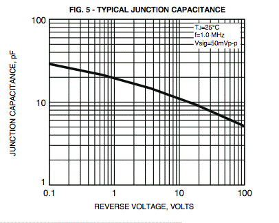
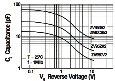
In place of R3 in the SAW Oscillator circuit, we inserted a 10 nH inductor in series with a 100-pF capacitor and a reverse-biased 1N4001 rectifier diode. The 100-pF has negligible impedance at 900 MHz. According to the graph above, the 1N4001 will present a 15-pF capacitance when reverse-biased by 3 V. A 15-pF resonates with 10 nH at roughly 400 MHz, at which point the phase shift of the two in series is close to zero. Our idea was to change the capacitance of the diode by varying its reverse bias. With a slight forward bias, we expect the diode's capacitance to rise to around 100 pF, at which point the impedance of our SAW filter coupling will be close to 90°. With a slight forward-bias, the phase shift will drop to something like 60°.

We bias the diode with two 1-kΩ resistors. We apply a voltage to the MOD input and measure the oscillator output frequency.
| MOD (V) | Frequency (MHz) |
|---|---|
| −1.0 | 900 |
| −0.8 | 901 |
| −0.6 | 902 |
| −0.4 | 903 |
| −0.2 | 903 |
| 0.0 | 903 |
| 0.2 | 903 |
| 0.4 | 903 |
With the diode forward-biased (MOD = −1.0 V), the diode presents a large capacitance. The 10-nH inductor dominates the coupling network. The oscillation frequency is 900 MHz, which is consistent with our earlier observations. With the diode reverse-biased, the diode presents a capacitance of around 15 pF. The frequency rises to 903 MHz. We know from previous observations that a 15-pF capacitor alone would give us an oscillation frequency of 910 MHz. Here the phase shift of the coupling network is somewhere between that of a 10-nF inductor alone and a 15-pF capacitor alone.
We apply a square wave to MOD. Our modulation of the output frequency is slowed down by the time-constant of the 1-kΩ resistors and the diode capacitance. We drop the resistors to 100-Ω. Now, of course, we are loading the coupling network and the SAW input. But we press on. To measure the change in output frequency, we need some kind of frequency-to-amplitude conversion. We use our BNC 21-MHz low-pass filter in series with our downshifted oscillator output frequency. The downshifted frequency varies from 35 to 43 MHz, so we get attenuation of 43 MHz with respect to 35 MHz in the filter. Below is what we see.
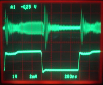
It appears to take around 200 ns for our A3014SO to settle to a new output frequency. If our SAW oscillator is to be a viable candidate for use in the 5-MHz modulation of one of our subcutaneous transmitters, it will have to settle to a new frequency in 50 ns.
We discovered elsewhere that the passband of the AFS915S3 is not 915±4 MHz, but 900−930 MHz. A 30-MHz passband can support frequency modulation at up to 15 MHz. In theory, there is nothing to stop the A3014SO with AFS915S3 from modulating its output frequency at 5 MHz or higher. The fact that it turns on and settles to its final output frequency in only 100 ns when we switch its power supply is itself a sign of 5-MHz modulation. We resolved to get some low-value capacitors and inductors, and to invest in some variable-capacitance diodes (varactors).
The AFS915S3 SAW filter has the phase response shown above. It's phase shift varies linearly from +180° at 897 down to −180° at 930 MHz. For every 10° by which we change the phase of the feedback path, the A3014SO oscillation frequency will change by 1 MHz. The AFS915S3 is not suitable for a compact SAW filter, because it requires long feedback traces to add phase shift to the oscillation loop. But we can assume that the magnitude of the slope of its phase response is typical of SAW filters, and so use the AFS915S3 to test a variable-phase coupling network.
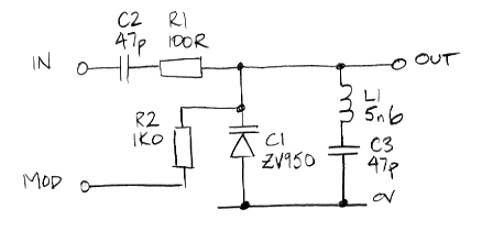
The Tank_Coupler page of our spreadsheet allows us to calculate the phase of OUT with respect to IN for various component values. We assume the SAW input looks like a pure 50-Ω resistor at 900 MHz. We let R1 be 100 Ω so that is will develop a phase shift with the tank circuit, but will not attenuate the oscillation by more than a factor of two. We choose L so it will resonate with C1 at around 915 MHz. We let C2 and C3 be 47 pF so that its impedance is far lower than that of the other components. We let R2 be 1 kΩ so that it looks large compared to the high-frequency impedances, but still has a short 47-ns time constant with C2.
We now consider the effect of MOD, assuming a ZV950 in place of C1. As we increase MOD from 0V to 2.7V, C1 decreases from 15 pF to 4 pF. According to our spreadsheet, the phase of our coupling network at 915 MHz will vary from −54° to +11°. When combined with the 10 °/MHz slope of a typical SAW filter phase response, we expect this 65° phase change to modulate the oscillation frequency by 6.5 MHz.
In theory, our tank coupler, combined with the UPC2746 amplifier and AFS915S3 SAW filter could provide the RF power for a battery-powered subcutaneous transmitter. The existing A3013 transmitter uses five P0603 packages (R4..R8 in the schematic) and one MSOP-8 (U3) to provide RF power and modulation. The tank coupler requires five P0603 packages, one SOD-523 (ZV950), one SOT-363, and one SAW-3MM. We assume we can power the amplifier with ten parallel outputs from the transmitter's logic chip, so we don't add another footprint for a power switch.
An alternative to using a tuning circuit is to use an RF switch and two PCB tracks of different lengths. We switch between the tracks and so change the phase shift of the feedback loop. A 50-mm difference in length gives us a 100° difference in phase. Assuming we use the UPC2746 as our amplifier, its phase shift will be −170°. We could tracks of length 70 mm and 120 mm to give phase shifts of ±50° outside the SAW filter. When combined with the AFS915S3, the graph above implies we will get oscillation frequencies of 905 MHz and 920 MHz.
It's hard to see how we could fit a 120-mm track on a small transmitter. We can avoid the long tracks and improve our ability to drive an antenna by adding another amplifier. With two UPC2746 amplifiers in series, we have a natural phase shift of +20°, which gives us a frequency of around 912 MHz. By switching to a 35-mm track between the two amplifiers, we subtract 70° from the phase, and so increase the oscillation frequency to 920 MHz.
This circuit attempted to use Zeltek's SA248 adaptor to connect a Lattice Semiconductor J-TAG programming interface to a bare 48-pin TQFP (thin quad flat-pack) chip.

We assumed that pin 1 on the SA248's DIP-48 footprint corresponded to pin 1 of the TQFP-48. We were wrong. Pin 1 on the DIP-48 corresponds to pin 42 on the TQFP.
| DIP-48 Pin | TQFP-48 Pin |
|---|---|
| 7 | 1 |
| 8 | 2 |
| 24 | 18 |
| 25 | 19 |
| 31 | 25 |
| 43 | 37 |
| 48 | 42 |
| 1 | 43 |
| 6 | 48 |
Because of our mistake, the board does not program chips. We will have to remove the adaptor and correct the layout if we want to program TQFP-48s in this way.
This circuit uses a MAX2624 to produce −3 dBm anywhere from 875 MHz to 1050 MHz.
The A3014MT circuit works well, and is far more convenient than our earlier A3001A. We did destroy one MAX2624 by applying too large a waveform to the modulation input, and taking TUNE down below −1 V. We added a zener diode from TUNE to 0V to clamp it between −0.6 V and +3.9 V.
We measured the output of two A3014MTs using our ZAD-11 mixer, as described here. Both appeared to produce around −7 dBm. This is 4 dBm below the −3 dB advertised in the MAX2624 data sheet. Perhaps this reduced power is caused by inadequate power-supply decoupling, as we observed here in the Subcutaneous Transmitter (A3009).
We tried various changes in the MAX2624 decoupling, and measured the A3014MT output power with our ZAD-11. In the table below, we record the peak-to-peak IF output voltage, as well as the A3014MT power it implies.
| Decoupling | IF (mV p-p) | A3014MT Output Power (dBm) | |
|---|---|---|---|
| 0 pF as C14 (rely on C11 and C12 70 mm away) | 75 | −10.6 | |
| 100 pF Panasonic ECJ as C14 | 117 | −6.7 | |
| 100 pF Panasonic ECJ on chip | 154 | −4.3 | |
| 1 nF TDK C2012X7R1H102K on chip | 140 | −5.1 | |
| 10 nF TDK C2012X7R1H103K on chip | 145 | −4.9 | |
| 100 nF Unknown on chip | 148 | −4.7 | |
| 1 μF Murata GRM on chip | 148 | −4.7 | |
| 47 pF Murata GQM as C14 | 126 | −6.0 | |
| 47 pF Murata GQM on chip | 160 | −4.0 | |
| 100 pF Murata GQM on chip | 151 | −4.5 | |
| 22 pF Murata GQM on chip | 151 | −4.5 | |
| 10 pF Murata GQM on chip | 123 | −6.3 |
| TUNE (V) | IF (MHz) | RF (MHz) |
|---|---|---|
| 0.1 | 53.3 | 883 |
| 0.2 | 36.2 | 892 |
| 0.3 | 28.1 | 900 |
| 0.4 | 23.4 | 907 |
| 0.5 | 19.6 | 915 |
| 0.6 | 16.8 | 924 |
| 0.7 | 15.3 | 929 |
| 0.8 | 14.0 | 935 |
| 0.9 | 12.8 | 942 |
We calibrated our A3014MT Serial Number 1 by downshifting its output using an 864±1 MHz Local Oscillator and measuring the IF frequency on our oscilloscope for a range of TUNE voltages. The table above gives this calibration.
[28-DEC-12] We replace the VCO on A3014MT#1 and calibrate both #1 and #2. Power output is −5 dBm and −6 dBm respectively. We use an 868 MHz local oscilattor and ZAD-11 mixer. We measure the intermediate frequency and so deduce the VCO output frequency.
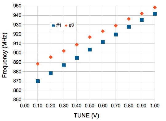
We adjust the tuning potentiometer on each board so as to place its frequency near 910 MHz.
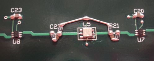
We started by building the RF amplifier with SAW filter and mixer: U7, L5, U8, and L6. We used the our 864-MHz A3014SO (AFS869S3 with capacitive coupling) to drive the LO input of the mixer. We shorted the RF input (J6) to ground with a 50-Ω terminator. At the IF output of L6 we observed a 100 mV, 20 MHz signal. When we touched the amplifier the frequency changed. With copper tape over the amplifier, the IF was 100 mV and 100 MHz. We were able to vary the frequency by moving our hands and touching parts. But we could never get the frequency into the range 30 MHz to 70 MHz.
With our 864 MHz LO, we downshift the nominal 902−928 MHz pass band of the SAW filter to 33−64 MHz. It appears that our RF amplifier is oscillating at frequencies outside the SAW filter pass band, never within it. We experienced something similar in our A3014SO, but in that case, the output of the amplifier was being fed back to the input.
We considered our decoupling capacitors. Our schematic called for 1 nF decoupling capacitors for U7 and U8. We found a report on parasitic inductance in surface-mount capacitors. It appears that all our P0805 capacitors are burdened with a minimum 1-nH inductance. At 1 GHz, this inductance presents an impedance of 6 Ω. The following graph is from another report. It shows capacitor impedance versus frequency for various capacitor values, assuming that the capacitor's parasitic inductance is 1 nH.

We have no reason to believe that our general-purpose capacitors achieve this minimum series inductance. But we are confident that the series inductance decreases with decreasing capacitance. Given that the impedance of a pure 100 pF capacitor at 900 MHz is less than 2 Ω, while its absolute minimum impedance due to its series inductance is 6 Ω, there seems little point in using a capacitor larger than 100 pF. (You will find more about capacitors and series inductance in our later work on the RF Combo (A3016).
The inductance of the 1 nF capacitors, combined with the inductance of our power supply leads, might have caused fluctuations to propagate around and cause oscillations. But if that were the case, why didn't we see oscillations within the SAW filter pass band? We replaced all the 1 nF capacitors with 100 pF capacitors. The parasitic oscillations persisted.
We inserted resistor networks between both sides of the SAW filter and the RF amplifiers, as shown below. Each resistor network acts something like a -8 dB 50-Ω attenuator. The parasitic oscillations stopped.
The UPC2764 oscillates when its source or load impedances deviate too far from 50-Ω. The source impedance seen by U8 at the SAW filter output is far from 50 Ω outside the SAW filter pass band. So U8 oscillated at some frequency outside the pass band, and never within the pass band.
We confirmed this theory with an application engineer at Minicircuits. He said that their MAR-6SM+ amplifiers (which we used in our A3005C receiver) will oscillate if the its source or load impedances deviate sufficiently from a pure resistive 50 Ω. He said 3-dB 50-Ω attenuators placed between any load or source and the output or input of a MAR-6SM+ would be sufficient to stop such oscillations. The ERA-3SM, however, is unconditionally stable.
With this network in place, we applied our 910-MHz A3014SO output to the RF input at J6. The +16 dBm input power destroyed U7. We replaced U7 and added a 12-dB attenuator in series with the A3014SO output. Our IF was 46 MHz. We added L7, the low-pass filter. The 46 MHz amplitude at the output of L7 was 100 mV, or 70 mV rms, or -10 dBm. The mixer's conversion loss is about -7 dB at 900 MHz, so our RF power is probably -3 dBm.
We apply the output of our A3014MT directly to the RF input at J6 using a BNC cable and no attenuator. The A3014MT output should be around −3 dBm, which is the typical power output of a MAX2624 powered at +5 V. Here is the IF output with A3014MT TUNE voltage.
We add a 12-dB attenuator in series with our A3014SO LO signal, and we obtain the following result, which shows that conversion loss is just as low, but more uniform, when we reduce our LO power from +16 dBm to +4 dBm. The mixer is designed for +7 dBm.
We insert a 36-dB attenuator in series with the RF input at J6. The IF output in the SAW pass band is around 100 mV. Additional attenuation reduces amplitude. If the output of the A3014MT is −3 dBm, then the input at J6 is −39 dBm. The output of the mixer is −10 dBm, so we expect the output of U8 to be around −3 dBm. Our amplifier and SAW filter provide a gain of roughly 36 dB. Given that the SAW filter has an insertion loss of at least 2 dB, and our two resistor networks each attenuate by 8 dB, our measurements suggest that U7 and U8 together provide a gain of 54 dB, or 27 dB each, which is higher than the 18 dB suggested by the UPC2746 data sheet. We attenuate the RF signal, and suddenly the IF disappears. We disconnect the RF power, leaving the attenuators on, and the IF comes back, but this time at 100 MHz. We conclude that our RF amplifier, consisting of U7 and U8 is unstable. The antenna or RF cable impedance can provoke oscillations in U7, and the SAW filter impedance itself comes close to causing oscillations in U8.
When we add U9 and U10, we find the output of U9 is a 0.5-V square wave, or +7 dBm. The absolute maximum input power of the UPC2764 is +0 dBm. We find that U10 is damaged. We conclude it has been damaged by excessive input power. We cannot build a limiting amplifier out of the UPC2764 without attenuators between stages. We connect the output of U9 to C33, the input of the Discriminator. We look at the amplitude at the top of C34. We adjust our A3014MT frequency until the amplitude on C34 reaches a peak. This peak occurs when C34 and L10 resonate together.
f = 1/2π√(LC)
Here f is the resonant frequency, and L and C are the values of L10 and C34 respectively. We measure the frequency on our oscilloscope, and find it to be 45 MHz. The nominal values of L10 and C34 were 100 nH and 100 pF, so the nominal resonance frequency is 50 MHz.
| C34 | f (MHz) | Comment |
|---|---|---|
| 47 | 62 | 47 pF axial through-hole |
| 50 | 60 | two 100 pF P0805 in series |
| 57 | 56 | 47 pF axial through-hole and 10 pF P0805 |
| 60 | 55 | two 100 pF P0805 in series, and one 10 pF P0805 in parallel |
| 100 | 45 | 100 pF P0805 |
It may be that our 100 nH inductor is closer to 125 nH, but it's a 10% inductor. It may be that our probe is disturbing the resonance. When we added U12, we found that the peak output at U12-1 occurred at a slightly higher frequency than we observed on C34.
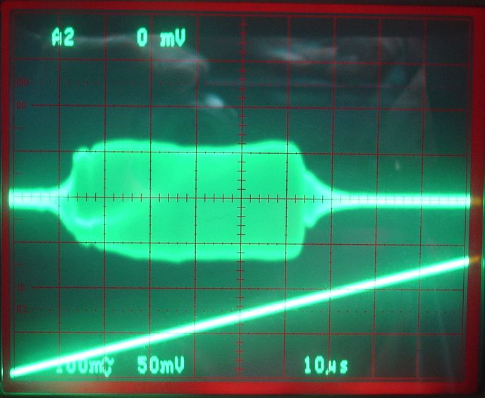
We built the diode demodulator, D1−D4, and found that it worked well. Here's the output from the A3014DR, J8, connected to our oscilloscope with a coaxial cable and a 50-Ω termination. We have 20 MHz bandwidth limiting on the scope traces, to remove the residual IF frequency.
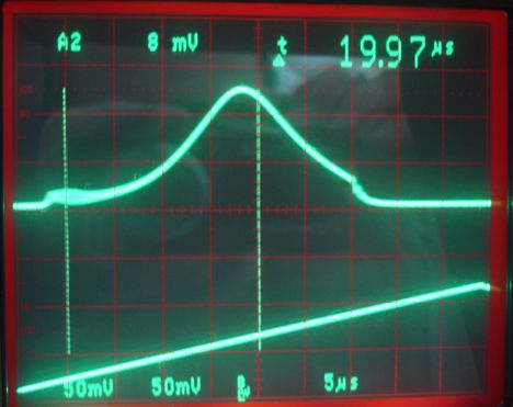
The demodulated output plot shows good response within the ISM band.
We measured IF frequency and amplitude for a range of TUNE inputs, as shown below. We attenuated the RF input to the A3014DR by 36 dB, so that the RF amplifiers would not saturate. The IF amplitude is an indication of the SAW filter attenuation. At each value of TUNE, we determine RF frequency from IF frequency by adding our LO (local oscillator) frequency. Our LO frequency is 864 MHz.
| TUNE (V) | IF Frequency (MHz) | RF Frequency (MHz) | IF Amplitude (mV) |
|---|---|---|---|
| 0.15 | 25 | 889 | 30 |
| 0.20 | 28 | 892 | 90 |
| 0.25 | 31 | 895 | 100 |
| 0.30 | 36 | 900 | 110 |
| 0.40 | 44 | 908 | 110 |
| 0.50 | 51 | 915 | 110 |
| 0.60 | 57 | 921 | 110 |
| 0.65 | 61 | 925 | 110 |
| 0.70 | 64 | 928 | 110 |
| 0.80 | 70 | 934 | 110 |
| 0.85 | 74 | 938 | 110 |
| 0.90 | 79 | 943 | 30 |
Our B3588 SAW filter pass-band appears to be roughly 900 MHz to 940 MHz. Its center is at 920 MHz, not 915 MHz. All our previous measurements, we have assumed that the center of the B3588 pass-band was 915 MHz. Our Demodulating Receiver (A3005C) was sensitive to signals all through the pass-band, which meant it was sensitive to signals between 930 MHz and 940 MHz. In the UK, the 930−940 MHz band is used for cell phones. The spectrum we took in Guildford, UK, shows how our transmitter signal overlapped the cell phone signals. This overlap was the 930−940 MHz band.
We can try to reject the power we receive above 930 MHz. The SCLF-65 filter from Minicircuits, in place of the SCLF-95 for L7 should do the trick. Its 3-dB point is around 70 MHz, and its 20-dB point is 80 MHz.
We conclude that we need to re-design our RF amplifier with stable gain stages, and insert attenuators between each stage as a guarantee of stability. The gain stages should be robust, and unable to destroy one another. Our IF filter needs to cut off sharply at the top end of the ISM band. Our discriminator and demodulator work well, but we would like to add a filter to eliminate the second harmonic of the intermediate frequency.