Test Transmitter (A3020)
© 2010, Kevan Hashemi,
Open Source Instruments Inc.
Contents
Description
Design
Hall Effect Switch
Current Consumption
Amplifier and Filter
Noise
Programming
SAW Oscillator
Modifications
Description
The Test Transmitter (A3020) is a combination of three circuits. Its purpose is to allow us to test the Subcutaneous Transmitter (A3019) and to investigate SAW (surface acoustic wave) VCOs (voltage-controlled oscillators). The A3020 contains the complete A3019 circuit in its center section. The circuit is almost identical to that of the Subcutaneous Transmitter (A3013). The most significant changes are as follows.
- Replace reed switch with Hall Effect Switch. The old magnetic switch was easy to break and large, not to mention its being discontinued by the manufacturer.
- Magnet turns off all power to circuit except Hall Effect Switch. The transmitter is either ON or OFF. When it's OFF, the only current drain is the Hall Effect Switch. When it is ON, it is transmitting.
- One input channel only, this saves us one op-amp.
- Two op-amps used for amplification and filtering instead of three. We reduce the DC gain of the main amplifier stage by adding a capacitor to its feeback loop. The capacitor sets the lower limit of the operating bandwidth at around 1 Hz.
- Power supply decoupling done so as to favor analog circuits. We use the battery and regulator directly for analog circuits, and supply current to the digital circuits and VCO through resistors that keep transmission noise off the analog supplies.
The SAW VCO circuits continue the earlier work we did with our RF Tester (A3014) and RF Combo (A3016) circuits. In the new SAW circuits, we are able to vary the feedback track length in order to provoke oscillations, and we are able to short a stub track to ground in order to cause phase changes.
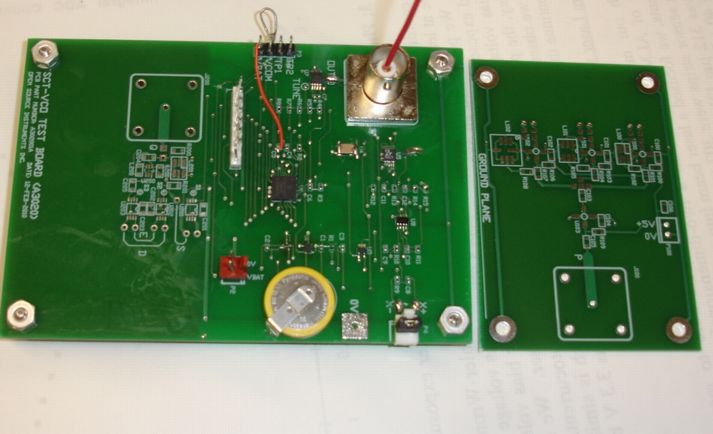
Figure: The A3020A Circuit. The middle section provides the circuit drawn in S3020_1, the test transmitter. The right section, which we have cut off because it is independent, provides S3020_2, the SAW oscillator. The left section uses signals from the logic chip in the test transmitter, and provides S3020_3.
In the following sections we chronicle our work debugging the A3019 circuit and seeing if we can get a SAW oscillator to provide frequency modulation.
Design
S3020_1: Subcutaneous Transmitter.
S3020_2: SAW Oscillators with Variable Track Length.
S3020_3: SAW VCOs with RF Switches.
Firmware: Logic Chip Firmware Library.
Hall Effect Switch
[26-FEB-10] The Hall Effect Switch consists of R1, C1, U1, U2, and C2 (see S3020_1). Component U1 is a A1171 Hall Effect sensor. Its quiescent consumption is a few microamps. It turns on for 80 μs out of every 60 ms (roughly 18 Hz switching). With R1 = 50 kΩ and C1 = 4.7 μF, we see a 100-mV linear drop on at U1-6 during the active period, or 1.2 V/ms, which indicates 5.9 mA out of C1. After the active period, the voltage on U1-6 rises with a time constant of around 30 ms, which is consistent with RC = 50 kΩ × 4.7 μF = 24 ms.
The average voltage drop across R1, meanwhile, is 280 mV when measured with a 10-MΩ, ×10 probe, indicating an average current of 5.6 μA. Our DVM measures 5.3 μA (after subtracting 0.2-μA offset). If we use a 1-MΩ, ×1 probe to measure the voltage drop, we see 420-mV drop because of current drawn by the probe, bringing the total to 8.4 μA. The current measured by our DVM increases to 5.6 μA when we touch R1 with the ×10 probe.
On VBAT, we see a 0.5-mV drop over 5 ms synchronous with the active period of U1. After that, VBAT rises 0.5 mV over 55 ms. At first, we had R1 = 1 kΩ, but with this smaller value we saw 50-mV of noise on VBAT as a result of the current surges through U1. We increased R1 to 50 kΩ. But we now find that U1 does not turn on reliably when we connect power. It will get stuck consuming 40 μA, with roughly 1.5 V across R1. We must short R1 with tweezers to get the chip to start up, after which it runs normally.
When we move a magnet near U1, it turns clocks U2, which is a D-type flip flop. The output of U1, which is U1-1, toggles between LO, or 0V, and HI, or VBAT. We use U1-1 as our source of power for the entire transmitter circuit, and decouple it with C2, a 4.7 μF capacitor.
The 18-Hz internal switching frequency of U1 is a potential source of 18-Hz noise in the transmitter amplifiers. With C1 and R1 functioning correctly, the amplitude of this noise at the input is less than 5 μA.
Current Consumption
[26-FEB-10] We measured current consumption at various stages of transmitter construction and programming.
| Components | Currrent |
|---|
| Off, switch only | 5.3 μA |
| Off, all components | 5.3 μA |
| On, switch, amplifier, clock | 9.9 μA |
| On, switch, amplifier, clock, dormant logic | 23.7 μA |
On, switch, amplifier, clock, dormant logic,
clock disconnected | 20.6 μA |
| On, switch, amplifier, clock, active logic | 42.9 μA |
| On, switch, amplifier, clock, active logic, RF VCO, no antenna | 74 μA |
| On, switch, amplifier, clock, active logic, RF VCO, 80-mm antenna | 76 μA |
| All components, transitting at full power. | 80 μA |
Table: Subcutaneous Transmitter Current Consumption. In each case we allow the circuit to settle fo 60 s before we record the current. We subtract an offset of 0.2 μA from our meter measurements to obtain the currents in the table.
Component U4 is the oscillator (see S3020_1). The oscillator produces CK, a 32.768-kHz, 1.8-V clock that connects to pins A7 and C5 of U6. When we break this connection, the current consumption of the circuit decreases by 3.1 μA. Component U6 is an LC4064ZC-75M56C programmable logic chip. It's the same chip in a BGA-56 package we used in the Subcutaneous Transmitter (A3009). In the Subcutaneous Transmitter (A3013) we used the same chip, but in a TQFP-44 package. The LC4064ZC has I/O capacitance 8 pF on pin A7 and clock input capacitance 6 pF on C5. Signal CK must fill and empty these capacitances 32,768 times per second, which accounts for a current of 14 pF × 1.8 V × 65536 /s = 1.7 μA. The remaining 1.4 μA could be explained by further gates within the logic chip buffering the signal into its global routing pool. We routed CK through A7 to the dedicated clock pin, C5, in order to penetrate the outer square of balls beneath the BGA-56 package. We resolve to break the connection between CK and C5, and use only pin A7. We expect this change to reduce the current consumption by roughly 1.5 μA. Given that total consumption is around 75 μA in the finished transmitter, we see that this simple omission of one connection will give us a 2% increase in battery life.
[01-MAR-10] We install the RF VCO, calibrate the firmware, and observe RF transmission. We install the ADC. Total current is now 80 μV. With a 48 mA-hr battery, we will get 600 hours of operation, or 25 days.
[07-MAY-10] Install a new 48 mA-hr battery and leave running.
[03-JUN-10] Circuit is still going, with battery voltage 2.48 V. That's 28 days so far.
[08-JUN-10] The circuit was not working today. So the battery life is something greater than 28 days = 672 hr. The measured quiescent current was 80 μA, so the battery capacity turned out to be 54 mA-hr, which is 10% higher than expected.
Amplifier and Filter
[26-FEB-10] The amplifier uses two op-amps. Both are contained in a single package, U8. The X+ input connects through 100 nF to the non-inverting input of the first op-amp, pin U8-5. Resistor R9 provides a DC path to the signal ground which is VCOM. We use VCOM for X− also. The transmitter is battery-powered and floating, so the X inputs present a pure, differential 10-MΩ impedance to high frequenies, and an infinite impedance to DC. The combination of C8 and R9 produces a single-pole high-pass filter with 3-dB frequency 0.16 Hz.
Resistor R10 and C9 control the gain of the first amplifier stage. Resistor R11 is fixed at 2 MΩ because of its involvement in the subsequent low-pass filter. The mid-frequency gain of the amplifier is 2 MΩ / R10. In our initial prototype, we use R10 = 50 kΩ, for a mid-frequency gain of 40. Capacitor C9 is 4.7 μF, and so produces a single-pole high-pass filter with 3-dB frequency 0.68 Hz, four times higher than the pole created by the input capacitor. This 0.68 Hz marks the low end of the transmitter's operating bandwidth.
The second op-amp provides a DC gain of 2.5. Combined with the first stage's gain of 40, we get a total mid-frequency gain of 100 from X to the input of U5, the sixteen-bit ADC. The ADC input range is 2.7 V, so we have a dynamic range of 27 mV at X. Each ADC count is 400 nV. The second op-amp provides the two imaginary poles of a three-pole 3-dB ripple Chebyshev low-pass filter. We measured and calculated the response of this filter when we applied it in the A3009, and again for the A3013. The plot below shows the low-pass filter combined with the C8-R9 and C9-C10 high-pass filters, with R10 = 50 kΩ.
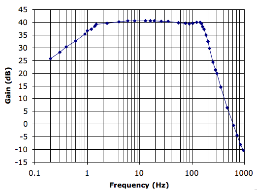
Figure: Gain versus Frequency for R10 = 50 kΩ. The nominal 3-dB frequency for the low-pass filter is 160 Hz. The nominal mid-frequency gain is ×100, or 40 dB. Note that both the gain and frequency axes are logarithmic.
With a gain of 40 dB, or ×100 in voltage, each ADC count is 2.7 V / 100 / 65536 = 400 nV.
Noise
[26-FEB-10] With no ADC (U5) or VCO (U7) installed, but the logic chip (U6) and the resitor DAC (R4..R8) installed, we see no sign of spikes on VBAT or VCOM, which shows that our new power supply decoupling is working. But we see the following noise upon the amplified X at U8-1 when we connect the X inputs with 0 Ω
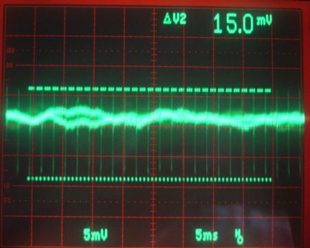
Figure: Noise on Amplified X with X Input Shorted and No RF or ADC.
Here we see what appears to be a combination of three noise signals. We have 2 mV p-p noise in the 1−160 Hz pass-band of our amplifier. We have less than 0.5 mV p-p white noise above the pass-band. And we have 15 mV p-p synchronous spikes from the logic chip activity.
The 2-mV p-p noise in the 1−160 Hz range corresponse to 20-μV p-p at the X input, or roughly 5 μV rms. The typical 0.1-Hz to 10-Hz noise at the input of U8 (see OPA2349) is 8 μV p-p, or roughly 2 μV rms. In the remaining 150 Hz of bandwidth, U8's noise density is 0.3 μV/√Hz, for another 4 μV rms. Adding these two noise signals in quadrature, we expect U8 to generate 5 μV rms in our 1−160 Hz bandwidth, which compares well to our observations. It appears that the noise at the output of our amplifier is U8's input noise.
The 15-μV p-p of synchronous noise is a potential problem. We turn off the resistive DAC by setting frequency_low and frequency step to 0 in the firmware. Now there is no current flowing through resistors R4..R8. The synchronous spikes drop to 4.0 mV p-p. With the DAC turned on again, we press our fingers against the DAC resistors and the synchronous spikes drop to 4.0 mV p-p. This 4.0 mV p-p is equivalent to 40 μV p-p at the X input. We will have to trust that our final transmitter layout with ground plane and short tracks will reduce the synchronous noise, and that what remains of it will have an effect less than our target input noise of 12 μV rms (that's what we obtained with the A3013A).
The high-frequency noise on the amplifier output is only 0.5 mV p-p, or 0.12 mV rms, which is equivalent to 1.2 μV at the X input. This 1.2 μV is insignificant compared to our existing 5 μV rms pass-band noise.
[01-MAR-10] We install the RF VCO and ADC and look at the noise on amplified X again. We see a large synchronous effect, as shown below.
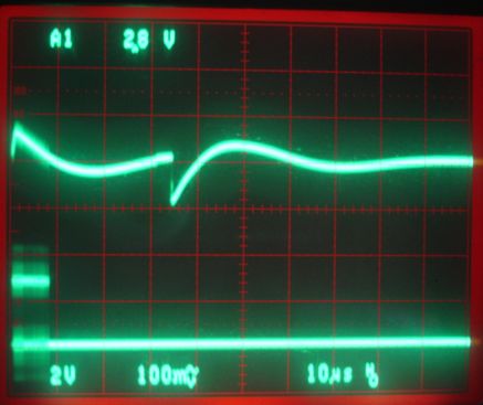
Figure: Noise on Amplified X with X Input Shorted and Full Transmission. Upper trace is the X input to the ADC, shown with 10 μs per division and 100 mV. The lower trace is the TP1 output, showing the transmission bits, with 2 V per division.
The sharp 100 mV drop at time 35 μs we also observe in the A3013A. The drop occurs when the ADC samples its X input. The sharp 80-mV rise at time 0 μs and subsequent roll we do not observe in the A3013A. In the previous circuit, we drove the ADC input with a ×11 gain stage with no filter function. In the A3020, we drive the ADC with the output of our low-pass filter (see schematic). The sharp changes occur in half a microsecond, suggesting a slew rate of 100 mV / 500 ns = 0.2 V/μs. The OPA2349 op-amp maximum slew rate is 0.02 V/μs. The jumps cannot be caused by amplification of noise spikes. Nor do we see spikes of this size upon the analog power supplies (see table below). We conclude that the sharp drops are a result of capacitors being connected to the op-amp output during the ADC's sampling process. Despite the alarming size of these jumps, they are synchronous with sampling, and will be common to all samples.
When we place the A3020A next to our receiving antenna, we see input noise of 20 ADC counts with X input shorted. Each count is 400 nV, so 20 counts rms is 8 μV rms input noise.
We remove the short and apply a 30-μV p-p 35-Hz square wave to X. We obtain the following plot of the signal, and its spectrum.
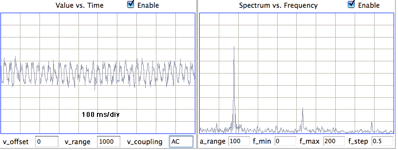
Figure: Neuroarchiver Display for 30-μV 35-Hz Square Wave Input.
The fifth harmonic has amplitude only 3 μV, and yet it is perfectly clear in the fourier transform of only a 1-s interval. The following plots we obtained with 10 MΩ across the X input. The tacks on the PCB pick up mains hum.
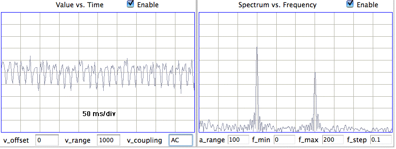
Figure: Neuroarchiver Display for 60-μV 60-Hz Mains Hum.
We see the first and second harmonic of an 80-μV 60-Hz hum. When we short the input, we get a spectrum that is, on average, flat with amplitude 3 counts, or 1.2 μV.
[01-MAR-10] We examine the power supplies, starting with 0V with a ×1 probe grouned to 0V, as a control. We move on to the other supplies, and fill out the table below.
| Supply | Spikes (mV p-p) | Ripple (mV p-p) |
|---|
| 0V | 1 | 0 |
| VBAT | 4 | 4 |
| 3V | 4 | 10 |
| 3VD | 50 | 50 |
| VCOM | 0 | 3 |
| 1V8 | 30 | 30 |
Table: Noise on the Power Supplies. Use ×1 probe grounded to 0V. The spikes and the ripple are synchronous with the transmitter active period of 1.953 ms.
The 3VD and 1.8V power supplies experience a rapid, linear drop during the 8-μs active period, followed by a damped return to their former value. If we assume each power supplies is decoupled by a perfect 4.7 μF capacitor, we conclude that the active current consumption is 30 mA from 3VD and 18 mA from 1.8 V. A total of 48 mA during 8 μs once every 1.953 ms suggests an average consumption of 200 μA. But our total current consumption is only 80 μA. It appears that our capacitors C6 and C4 have effective capacitance closer to 2 μF.
Programming
We cannot program U1 with a 1-kΩ resistor (R2 in schematic) in series with the 1.8-V power supply. The current required by the programming cycle is over 2 mA at times. Thus we connect P1-1 to 1V8 instead of VBAT. We use a jumper to short P3-1 to P3-2 (1V8 to VCOM) during programming. We remove the jumper afterwards to allow R2 to isolate VCOM from the digital noise on 1V8.
We copy A3013A05.able into A3020A01.abl. We re-assign pin names, remove reed switch code, change auxilliary channel to be 15 always in anticipation of slow data channel. We remove the reference transmitter code. We compile and find that the number of logic blocks required has dropped from 48 to 44. We have a batch of 100 LC4064ZC-75M56C chips (U6, cost $2.80 each). To obtain our 200-ns bit period, we set tcd_divisor = 27, half_tcd_divisor = 14. For RF calibration we set frequency_low = 8.
SAW Oscillator
The upper section of the A3020A is the SAW Oscillator (A3020SO). Its schematic is S3020_2. These circuits are RF amplifiers with SAW filters in a feedback loop so that oscillation will occur within the pass-band of the SAW filter. The ERA-3SM amplifiers are unconditionally stable, so we have no fear of parasitic oscillations outide the SAW filter passband. The SAW oscillators are layed out so that we can vary the feedback path length by adding wire links to solder pads.
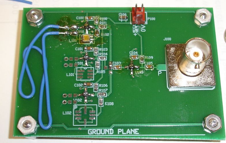
Figure: SAW Oscillator. The blue wire is a 150-mm addition to the feedback path length. The total path length is 178 mm.
We vary the feedback path length by inserting a wire cut to shorter and shorter length. We bend the wire back upon itself. It may be that the signal couples to itself where the wire is pressed against itself, and such coupling may have disturbed our measurements of frequency versus path length, shown below.
The A3020SO provides SAW-3MM, SAW-3.8MM, and SAW-5MM footprints. In the course of our experiments, we discovered we had the wrong pinout for the B3570 in the SAW-5MM package. This mistake we carried over from the A3014SO and A3016SO. The SAW filter ground connections are used for the signal while the signal connections are grounded.
| Part | Nominal Pass Band (MHz) | Package |
|---|
| AFS869S3 | 865.0-873.0 | 3.8-mm |
| AFS915S3 | 911.5-918.5 | 3.8-mm |
| AFS916.5S3 | 913.0-920.0 | 3.8-mm |
| B3563 | 862.5-865.5 | 3.0-mm |
| B3570 | 867.4-869.4 | 5.0-mm |
| B3574 | 867.3-869.3 | 5.0-mm |
| B3588 | 902.0-928.0 | 3.0-mm |
| B3715 | 868.0-870.0 | 3.0-mm |
Table: SAW Filters Used With the A3020SO.
We measure frequency with path length and plot for two sets of SAW filters: those with frequency around 868 MHz, and those with frequency around 915 MHz. We measure frequency by mixing the oscillator output with an LO of 910 MHz (when the oscillator is near 868 MHz) or 868 MHz (when the oscillator is near 910 MHz). We use the more distant LO so as to remove ambiguity in the IF output. Our mixer is the ZAD-11. Our LO sources are A3014SOs with B3588 for 910 MHz and B3570 for 868 MHz.
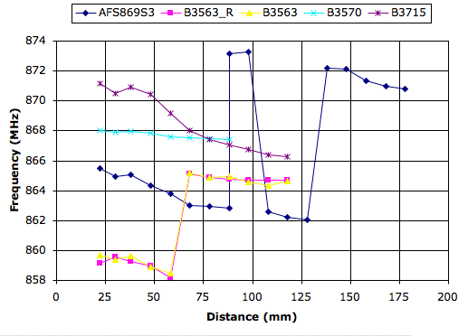
Figure: Oscillation Frequency versus Feedback Path Length for Various SAW Filters.
We see oscillation at exactly 686 MHz with the B3570 when the path length is the shortest possible. The B3563 is the filter we use in the A3018C, where it is soldered to an A3016SO in location L100 and provides 864-MHz for the demodulating receiver. The B3563 we tried in two orientations. In the A3563_R plot, we had pin 2 as the input instead of pin 5. We obtained the same result, and so conclude that SAW filters are symmetric. The AFS869S3 frequency is unstable for path lengths 80-110 mm. At 130 mm its frequency jumps by 10 MHz.
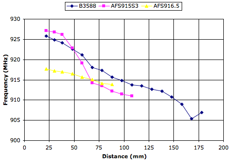
Figure: Oscillation Frequency versus Feedback Path Length for Various SAW Filters.
Our new circuit provokes oscillations in all three of the 902−928 MHz SAW filters we tried, but oscillations do not occur at certain path lengths. The B3588 behaves well all the way through its pass-band, with oscillation frequency falling uniformly from 925 MHz at the shortest path length, to 905 MHz at the longest.
The A3020SO uses a 5-V power supply for its four ERA-3SM amplifiers. Total current consumption is 140 mA. The power output at the oscillation frequency is +7 dBm, which we measure by placing a 6-dB attenuator in series with the output and downshifting with the ZAD-11, whose insertion loss is 7 dB. We see a 320-mV p-p output, or −6 dBm. We assume this +7 dBm is the maximum power output of the ERA-3SM with a 5-V power supply and 50-Ω bias resistor.
We now try the AFS869S3 with various feedback path and stub combinations. A stub is a line that leads nowhere, which we can either leave open-circuit at the end, or short to ground. If open-circuit, the incoming voltage wave will reflect with a 0° phase change. If short-circuit, the voltage wave will reflect with a 180° phase change. When it combines with the original wave at the base of the stub, we will get a different combined phase depending upon whether we short or leave open the end of the stub. We add a 100-pF capacitor in the feedback loop at either end of our path-stub combination. The stub path is a 2.54-mm copper tape with 1.6 mm of G4 circuit board between it and the ground plane. This 2.5-mm track makes a 50-Ω transmission line, with wave velocity 200 mm/ns. At 869 MHz (period 1.15 ns), we expect a 1.6°/mm phase change along the track, so that a 29-mm track will give a 45° phase shift. The round-trip will be −90° when the end is open-circuit. With the end shorted, the total round-trip will be +90°.
| SAW Filter |
Main
Path (mm) |
Stub
Path (mm) |
Termination
to 0V (Ω) |
Frequency |
| AFS869S3 | 30 | none | ∞ | 865.5 |
| AFS869S3 | 30 | 30 | ∞ | 864.1 |
| AFS869S3 | 30 | 30 | 0 | 866.2 |
| AFS869S3 | 30 | 45 | ∞ | 863.9 |
| AFS869S3 | 30 | 45 | 0 | 865.7 |
| B3588 | 30 | none | ∞ | 924.0 |
| B3588 | 30 | 45 | 0 | 923.4 |
| B3588 | 30 | 45 | ∞ | none |
| B3588 | 30 | 30 | 0 | 927.4 |
| B3588 | 30 | 30 | ∞ | 922.6 |
| B3588 | 30 | 17 | 0 | 929.1 |
| B3588 | 30 | 17 | ∞ | 921.9 |
| B3588 | 100 | none | ∞ | 912.0 |
| B3588 | 100 | 15 | 0 | none |
| B3588 | 100 | 15 | ∞ | 910.6 |
| B3588 | 100 | 30 | 0 | 918.6 |
| B3588 | 100 | 30 | ∞ | 909.7 |
| AFS915S3 | 30 | 30* | 0 | 928.3 |
| AFS915S3 | 30 | 30* | ∞ | 924.3 |
| AFS915S3 | 60 | 30* | 0 | 927.0 |
| AFS915S3 | 60 | 30* | ∞ | 922.7 |
Table: Effect of Stub upon Oscillation. The * paths are insulated wires instead of coper tracks.
With the B3588, a 100-mm feedback path, and a 30-mm stub, we can change the oscillation frequency from 909.7 MHz to 918.6 MHz by shorting the end of the stub to 0 V. We did this by hand with a wire, but in theory we could short the stub to ground with an RF switch, and so make a digital VCO.
With an AFS915S3 in position L101, we have oscillations at 913 MHz. We remove U103, the output buffer and connect C102 directly to C105. Output power drops from +7 dBm to 0 dBm. We replace R104 with 0 Ω and output power rises to 2.7 dBm. We replace R105 with 120 Ω. Output power remains unchanged.
With the B3588 we could make a ready-calibrated, temperature-stable, digital VCO switching in the 902-928 MHz ISM band. It would require a 100-mm feedback track, a 30-mm stub, the 3-mm SAW package, the RF amplifier, and an RF switch for the end of the stub. Compare this to our MAX2624, which we must calibrate to place its frequency in the ISM band, and which drifts at −0.4 MHz/°C. But the advantage of the MAX2624 is that it is one component. The current consumption of the A3016SO, if we eliminate three of the four amplifiers, is 35 mA for +2.7 dB, while that of the MAX2624 is 10 mA for −4 dB.
Modifications
Here we list modification to the test transmitter circuit that we expect to carry over in some form to the Subcutaneous Transmitter (A3019).
- Connect U4-1 to 1.8V in order to enable the oscillator. Leaving the input floating is not reliable.
- Increase R1 to 50 kΩ to remove U1 power spikes from VBAT.
- Change P3-1 to 1V8. Was previously VBAT. Allows us to short P3-1 to P3-2 for programming.
- Break connection from U1-3 to U6-C5. Use only U6-A7 for the CK input, to save on current.
Here are other modifications.
- Correct pinout of the SAW-5MM. Should have L102 input as pin 5 and output as pin 1.