Command Transmitter (A3029)

© 2014-2023 Kevan Hashemi, Open Source Instruments Inc.

Contents

Description
Design
Firmware Versions
146 MHz Oscillator
915 MHz Oscillator
910 MHz SAW Oscillator
146 MHz Amplifier
915 MHz Amplifier
910 MHz Amplifier
Command Transmission
Power Measurement
Development

Description

[10-MAY-24] The Command Transmitter (A3029) will soon be replaced by the Telemetry Control Box (TCB-B16), which combines telemtry reception and command transmission on all its antennas, as well as providing four general-purpose digital input-outputs.

[27-JUL-22] The Command Transmitter (A3029) is a 1-W, 50-Ω, on-off modulated radio-frequency transmitter with a BNC socket for a transmit antenna. The A3029A produces 146 MHz and the A3029B produces 915 MHz. The A3029 is intended for use with our Implantable Sensors with Lamp (ISL), such as the A3024 and A3030. The A3030A and A3030B respond to 146-MHz commands, and are compatible with the A3029A. The A3030C responds to 915 MHz commands, and is compatible with the A3029B. The 146 MHz and 915 MHz command frequencies are accurate to ±0.01 MHz, which permits sharp, fixed tuning of the the ISL crystal radios.


Figure: 910-MHz Command Transmitter (A3029C) in Enclosure. The enclosure top is machined out of one piece of cast aluminum for better heat conduction and grounding. We see the LWDAQ branch cable and 24-V boost power cable entering on the left. Output power on the BNC socket of the enclosure is 1 W. A Loop Antenna (A3015C) provides omnidirectional transmission for implanted 910-MHz crystal radio receivers. There are four indicator lamps, from top to bottom: LWDAQ Power (green), Boost Power (blue), Activity (amber), and Transmit (white). For the 146-MHz Command Transmitter (A3029A), see here.

The A3029 can operate from the LWDAQ power supplies alone, in which case it produces its non-boost power output. The non-boost output is 240 mW into 20 Ω for the 910 MHz A3029C, but lower for the earlier versions. With a 24-V, 500 mA boost power supply connected, output power jumps up to 1 W into 50 Ω (+30 dBm) for all versions of the A3029. For the boost power supply we can use a power adaptor like the CENB1010A2403F01. The power adaptor must deliver 10 W at anything from 18-36 V on a 5.5-mm power plug. The connector can be wired with either polarity. With or without boost power, the A3029 output is unconditionally stable.


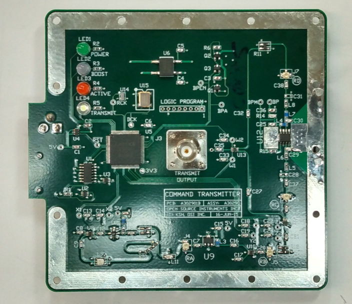
Figure: 910-MHz Command Transmitter (A3029C) Circuit, Top Side. Made with A302901B PCB. For bottom side with DC-DC converter and connectors see here.

The Transmit lamp turns on only when the antenna output is generating command power. The Activity lamp turns on when the A3029 is exercising some communication or stimulation function, even when it is waiting to transmit command power. The LWDAQ Power lamp indicates that power is being delivered by the LWDAQ cable. The Boost Power lamp indicates the boost power is available.

Version Oscillator
Type
Frequency (MHz) Non-Boost
Power (W)
Boost
Power (W)
A3029A Crystal 146.000 MHz 60 mW 1.0 W
A3029B Crystal 915.000 MHz 100 mW 1.0 W
A3029C SAW 910 MHz 240 mW 1.0 W
A3029F None None None None
Table: Versions of the Command Transmitter (A3029). The A3029F is a repurposing of the logic on the A3029 for command transmission over a wired serial interface.

The A3029 uses a fixed-frequency oscillator to produce its output frequency. We cannot sweep the oscillator frequency. We can, however, inject power from a radio-frequency sweep into the intermediate and power amplifiers so as to measure their frequency response and adjust their matching networks. We use the Command Transmitter (A3023CT) to produce sweep frequency around 146 MHz and the Modulating Transmitter (A3014MT) for sweeps around 915 MHz.

The A3029 radio-frequency amplifier consists of two stages and four switches. The switches perform on-off modulation and select automatically between the boost and non-boost output depending upon whether we have the 24-V boost power connected.

Design

S3029_1: Logic and Boost Power Input for A3029A/B/C.
S3029A_2: 146-MHz Oscillator and Power Amplifier for A3029A.
S3029_3: 915 MHz Crystal Oscillator for A3029B.
S3029B_2: 915-MHz Power Amplifier for A3029B.
S3029C_2: 910-MHz Oscillator and Power Amplifier for A3029C.
A3029C.ods: Bill of Materials for A3029C.
Code: Firmware for the logic chip, Jedec compiled files and ABEL source files.
A302901A.zip: PCB Version A Gerber, Main.
A302902A.zip: PCB Version A Gerber, 915 MHz Oscillator.
A302901B.zip: PCB Version B Gerber, Main, for A3029C.
A302901B.dxf: Drawing of A302901B PCB.
A302901B_Top: Top view drawing of A302901B.
A302901B_Bottom: Bottom view drawing of A302901B.
A302902B.png: PCB Version B View, 915 MHz Oscillator, for A3029B.
A302902B.zip: PCB Version B Gerber, 915 MHz Oscillator.
A302902A.png: PCB Version A, 915 MHz Oscillator, for A3029B.
A3029A.easm: Solid Model of circuit and enclosure.
A3029A_Top.pdf: Drawing of enclosure top.
A3029A_Base.pdf: Drawing of enclosure base.
SI-510: Programmable oscillator, 146.000 MHz.
SI-590: Programmable oscillator, 457.500 MHz.
MGA-31189: Amplifier, 21 dB gain, 250 mW output.
RFPA-3800: Amplifier, 18 dB gain, 5 W output.

Firmware Versions

[10-FEB-17] Firmware version P3029C01.abl configures the A3029C as a command transmitter for the Implantable Sensor with Lamp (A3030). The A3029C provides three operations through LWDAQ commands. The rf_on operation turns on continuous RF power. We execute this operation by sending LWDAQ command "0081" to the A3029C. The rf_off operation turns off continuous RF power. We send "0000" to turn off the RF power. The rf_xmit operation transmits the upper eight command bits as a serial byte using the ISL command transmission protocol. We execute this operation by sending LWDAQ command "XX82", where "XX" is the hexadecimal representation of the eight-bit value we want to transmit. We describe the transmission protocol here. The bit period is 8192 bits/s, with ten bits being used for each byte transmission. A start bit of 1 is followed by the eight data bits, then a stop bit of 0. At the end of the transmission, the RF power remains off until another command to turn it on is issued. Even if the RF power were turned on continuously before the byte transmission, it remains off afterwards, but boost power will remain connected to the 1-W amplifier unless we follow with a shut-down command "0000".

Earlier versions of the firmare work with earlier versions of the circuit board. The P3029B01 firmware configures the A3029B 915-MHz command transmitter to work with the Implantable Sensor with Lamp (A3030C/D). The P3029A03 firmware configures the A3029A as a command transmitter for the Implantable Sensor with Lamp (A3030A/B). The P3029A02 firmware configures the A3029A to to emmulate a Command Transmitter (A3023CT) and Lamp Controller (A2060L). We generate periodic pulses and finite-length stimuli from this firmware with the Lamp Controller tool.

[02-FEB-23] The A3029F01.abl code re-purposes the A3029 for command transmission using the same on-off protocol, but using the X1 logic signal as the outgoing carrier, rather than a radio frequency burst. All the RF amplifiers are disabled by removing their current delivery inductors and resistors. Current consumption is 27 mA from +5 V and 0 mA from ±15 V.

146 MHz Oscillator

[22-APR-14] We have 10 of the SI-510BCA-146M000-BAG crystal oscillator programmed to 146.000 MHz. The oscillator comes in a 3.2 mm × 5.0 mm DFN-6 package is supposed to be accurate to ±30 ppm, takes 3.3-V power and produces a 100-Ω LVDS output. We assemble the following circuit.


Figure: Oscillator Test Circuit Schematic.

The photograph below shows our hand-wired and epoxy-potted assembly on an old antenna board, with a BNC connector on the back.


Figure: Oscillator Test Circuit Assembled.

We connect 3.3-V power to our circuit. The oscillator draws 20 mA. We connect the output to our oscilloscope with a 1-m coaxial cable and terminate with 50 Ω. We get a 380-mVp-p square wave, frequency 145±1.5 MHz. We connect a BLP-150 coaxial 150-MHz low-pass filter directly to the oscillator. We connect the filter to our oscilloscope with a 1-m coaxial cable. We obtain a sinusoid of amplitude 380 mVp-p, or −4.4 dBm.

In the command transmitter circuit, we will use the LFCN-160 160-MHz low-pass filter with insertion loss similar to the BLP-150 at 146 MHz. We will amplify the −4.4 dBm sinusoid in two stages: first by 21 dB with the MGA-31189 and then by 18 dB with the RFPA-3800. We can accommodate 5 dB in stabilizing attenuition and other losses, and still get 30 dBm at the antenna output.

[14-MAY-14] We receive our A302901A circuit board. We load the 146-MHz SI-510 into position U7. With R8 = 0.1 Ω, C9 = 1.0 nF, and R7 and C8 omitted, we divert the output of L2, a LFCN-160 low-pass filter, to our auxiliary BNC connector, and observe −2.4 dBm. The insertion loss of L2 at 146 MHz is around 0.8 dBm, so U7 generates −1.6 dBm.

915 MHz Oscillator

We plan to use an SI-590 at 457.5 MHz, followed by an AMK-2-13+ frequency doubler, a UPC2746 amplifier, and a 2-dB attenuator to produce 3 dBm of unconditionally-stable 915.000 MHz. This we will connect to U9 with switch U8 when we want to tansmit command power at J3.

[19-MAR-15] We receive our A302902A printed circuit board, which implements our 915 MHz oscillator, schematic S3029_3. We load all components, including BNC-V for J1. We have to bend the leads up on U2 and load it upside down because we have the pinout reflected on the A302902A printed circuit board. We supply 3.3 V and measure 110 mA quiescent current. We connect −20 dB to J1 and mix the result with our 910 MHz SAW Oscillator (A3014SO). We get IF −20 dBm of 4.0 MHz added to −34 dBm of 446 MHz. The oscillator produces +7 dBm of 915 MHz and −7 dBm of 457.5 MHz. The SI-590 is accurate to ±25 ppm, so our 915 MHz output should be accurate to ±25 kHz. Our 910 MHz oscillator is closer to 911 MHz. We call our oscillator crystal oscillator the A3029XO-915.


Figure: A3029XO-915 Crystal Oscillator. According to our vector voltmeter, its output power is 14 dBm. According to our mixer-based power measurement, its output is 11 dBm.

We connect the output of the A3029XO-915 to the auxiliary input of our A3029B prototype. We run the transmit output through −33 dB and mix with 910 MHz. We measure +27.2 dBm of 915 MHz added to +0.4 dBm of 457.5 MHz. We touch the A3029B first amplifier stage and get 28.5 dB out. We mix the A3029XO-915 output with our 868 MHz SAW Oscillator (A3024SO) and get 47.0 MHz IF.

[21-APR-15] We run the output of our A3029XO-915 through a ZB4PD1-2000 four-way coaxial splitter. We measure amplitude at one port with our vector voltmeter probe and a 50Ω terminator and get 538 mV rms, or 7.6 dBm, which implies A3029XO output 14 dBm. We measure amplitude on another port with your second vector voltmeter probe, a ×10 dividor, and a 50-Ω terminator, and get 54 mV rms, which also implies 14 dB at the A3029XO. We pass the output from another port through −10 dB, mix in our ZAD-11 with 868 MHz, and get IF 155 mV pp of 45 MHz, which implies +11 dBm at the A3029XO.

For comparison, we replace the A3029XO with our A3014MT and repeat the same three measurements. We get −2 dBm, −3 dBm, and −5 dBm respectively for the A3014MT output.

[01-MAY-15] We receive A302902B printed circuit boards with the U2 footprint corrected. We load parts on three of them. The amplifier oscillates, so we damp oscillations by placing 100 Ω J1 to 0V. We connect one A3029XO-915 to the underside of an A3029B, as shown below.


Figure: A3029XO-915 Crystal Oscillator Mounted on A3029B. A 15-Ω resistor connects +5 V to 3.3 V. We add a 1-μF decoupling capacitor where power enters. A 100 Ω resistor connects output to 0V on C4 to stop local oscillations. A 100-pF capacitor on U2 to stop oscillations caused by communication with the boost power amplifier.

When we connect the 120-mA current drain of the oscillator to the A3029B's 3V3 power supply, the 3V3 regulator becomes unstable. We connect the oscillator 3V3 to +5V through 15 Ω and add a 1-μF decoupling capacitor where power arrives on the oscillator circuit board. The maximum supply voltage will be 3.2 V. In practice, the +5V power supply will be around 4.6 V, so the circuit runs at 2.8 V. With boost power applied, oscillator's amplifier picks up the transmit output and oscillations far from 915 MHz start up. We place 100 pF in P0402 package across U2-5 and U2-6. The oscillations stop.

910 MHz SAW Oscillator

[13-JUN-15] The A3029XO-915 produces sub-harmonics, consumes 120 mA, and is vulnerable to parasitic oscillation. We welcome its precise 915.000 MHz frequency, but we can accept a ±2 MHz uncertainty in the command transmitter's output. Furthermore, the oscillator is always running, which means there is always the possibility of its power reaching the antenna. We decide to build a new circuit board, in which we incorporate what we have learned about the amplifier tuning, and we switch to a SAW-filter oscillator. The A3027D's local oscillator runs at 911 MHz when we load it with a B3588 SAW filter. This local oscillator is an ERA-3SM amplifier from which we take a small fraction of its output and feed it back to the input through a SAW filter and a delay line. The total length of the loop is 134 mm.


Figure: The 910-MHz SAW Oscillator on the A3029C. We have eliminated one of the bends in the feedback loop so as to reduce the feedback phase delay and raise the oscillation frequency. Final value for the feedback resistor is 30 Ω made out of three 10-Ω resistors in series.

The A302901A circuit board has four copper layer. The second layer is the ground plane, and lies a nominal 9.3 mils below the top layer. The radio-frequency signal traces on the A302901A are 16 mils wide. Their impedance is 51 Ω. Propagation velocity is 185 mm/ns. At 915 MHz, phase delay is 1.8°/mm.

We measured the B3588's phase shift versus frequency and plotted it here. The phase is 0° at 916 MHz and varies by −13°/MHz. The phase shift introduced by a delay line at 915 MHz is −2°/mm. Using the A3027D's oscillator as a starting point, if we want 915 MHz, we should decrease the total propagation length of the delay line by (915-911)*13/1.8 = 29 mm to around 105 mm, which is consistent with our observations with the A3020. By including an RF switch in the feedback loop, we believe we can start and stop oscillations within tens of nanoseconds. By turning on and off power, we observed a SAW filter oscillator turning on and off in only 50 ns.

[07-AUG-15] We received the A302901B circuit boards a few weeks ago, and load parts today, only to discover that the GM1 layer, which should be layer three with positive polarity, was made in layer three with negative polarity. We have no power distribution but we may be able to test the SAW oscillator.

[12-AUG-15] We apply 5-V power to our A3029C SAW oscillator. We bypass U8 with a wire link, since our A302901B circuit board cannot support logic with its faulty middle copper layer. With R10 = R9 = 100 Ω, we get parasitic oscillation at an unknown frequency, but within the range of our vector voltmeter. We reduce R10 to 0 Ω and get 908.5 MHz, 1.0 V amplitude, +13 dBm at J4, where we extract the signal using a coaxial cable, and we have removed C7. We lengthen our U8 bypass link by a few millimeters and get 908.1 MHz. We shorten it as much as we can and get 908.6 MHz. We cool with freezer spray and frequency drops to 906.5 MHz. We wash, dry, and heat with our heat gun. Frequency is 908.1 MHz. We bypass the R10-R9 loop, reducing the feedback path length by around 20 mm. Frequency is now 913.3 MHz.

[13-AUG-15] We apply 5.0-V power. We load L11, the LFCN-1000 1-GHz low-pass filter. We use the entire feedback loop with a wire bridge between the input and output pins of the U8 footprint. We replace our UMC cable because the socket on the end is damaged. We attenuate the RA output by 20 dB and mix with 869.4 MHz. We get 38.6 MHz, 65 mVpp. We connect the attenuated RA output to our vector voltmeter and get 84 mV rms. It looks like RA is +11 dBm at 908 MHz. Current from +5.0 V is 32 mA.

[17-AUG-15] We assemble a complete A3029C on our second batch of A302901B circuit boards. Firmware P3029C01.abl changes the polarity of X1 to suit the new arrangement. The oscillator produces 908.5 MHz. At RB we see 3.9 V rms (24.8 dBm) and after 2-dB attenuator at RC 3.0 V rms (22.6 dBm). For these measurements we remove R12 and C37 respectively to make sure all signal leaves via J5 and J6 respectively. With RFON unasserted, we find that U7 oscillates until we increase C10 from 1 nF to 1 μF. We send a square wave to the RFON signal. When we assert RFON, the feedback loop closes. On the scope we measure start-up time s 650 ns. Stop time is 50 ns.

[17-AUG-15] With switch U8 loaded, our SAW oscillator produces 906.4 MHz. We eliminate one of the bends in the feedback loop and the output frequency rises to 910.3 MHz (we are mixing with our 915.000 MHz source). We load the entire A3029C in its metal enclosure, with all mounting screws. Output frequency is now 910.0 MHz. We are using three 10-Ω resistors to eliminate the bend, so R9 and R10 in the schematic have been replaced by three 10-Ω resistors on the surface of the board.

146 MHz Amplifier

[30-APR-14] In the Octal Data Receiver (A3027) we used a top-layer coplanar waveguide with a bottom-layer ground plane. The result is attractive, but hard to lay out. We want to try something different in this circuit. We cut open two old 62-mil (1.57 mm) four-layer circuit boards and find they both have the same three-layer stack-up. We measure the top and bottom layers to be 12 mils (300 μm) and the center layer 39 mils (1.0 mm) thick. We consult with Advanced Circuits and find that they build four-layer boards of FR4 and copper like this. If we make the layer-two copper a ground plane, we will have 10 mil (250 μm) of dielectric between layer-one and the ground plane. Let us assume the relative permittivity of FR4 is 4.8. A 50-Ω top-layer microstrip waveguide will be 16 mils (460 μm) wide.

[14-MAY-14] We receive our A302901A circuit board. We load the RF switches (U8, U10, U11, U13, RF3024), the 2-dB attenuator (R12, LAT-2) and the first amplifier stage (U9, MGA-31189). With the switches set correctly, and a 1.0-μH ceramic inductor in place of L3 we get +15 dBm (3.7 Vp-p) of 146 MHz at OUT. This particular inductor, LQM21NN1R0K10D has self-resonant frequency of around 100 MHz. With the ceramic wire-wound 100-nH AISC-0805-R10J-T, self-resonant frequency 1200 MHz, in place of L3 we get +16 dBm (3.9 Vp-p). Assuming 0.15 dB insertion loss in U10, U11, and U13, and including the 2-dB attenuator, we see that U9 is generating roughly 19 dBm (5.3 Vp-p). After the insertion loss of U8, its input is around −2.5 dBm, so U9 is giving us gain of 21 dB, which agrees well with the data sheet.

We load RFPA-3800 in location U12 with 100 nH for L4. We omit C28-C31. We load 51 Ω for L5, 0 Ω for L6, 51 Ω for L7, and 0 Ω for L8. We have 1 dB attenutors for R17 and R18 and 0 dB for R19. With 49 mVp-p at U12 input we get 355 mVp-p at the output, for gain of 17 dB gain. We measure the phase and amplitude of the voltage on either side of our 51-Ω resistors, with respect to the signal on OUT, using a 10-MΩ probe. We have OUT connected to our oscilloscope with a 36" cable. At R13/L5 we have 142 mVp-p and −4.49 ns, at L6/U12 48.5 mVp-p and −5.42 ns, at U12/L7 355 mVp-p and −2.26 ns, at L8/R16 148 mVp-p and −1.95 ns.

[15-MAY-14] We note that L3 nd L4, 100 nH AISC-0805-R10J-T, have DC resistance 0.46 Ω and rated current 400 mA. With RF power on (the 146 MHz oscillator output is connected to U9), the A3029 draws 160 mA from +5 V. With RF power off, it draws 148 mA. The oscillator uses 20 mA and the logic chips another 3 mA, so the U9's quiescent current appears to be 125 mA. We attach boost power and measure 16 mV across R14 (0.1 Ω) with RF power off, so U12's quiescent current is 160 mA. We drop R15 to 500 Ω and quiescent current increases to 520 mA. After a few minutes, L4 and U12 are hot.

[16-MAY-14] We attach boost power and leave the RF power off. We measure the quiescent current of the RFPA-3800 (U12) with the help of resistor R14. We try various values of bias resistor (R15). The boost power is +5.0 V throughout.


Figure: RFPA-3800 Quiescent Current versus Bias Resistance. Power supply is +5.0 V.

We choose 767 Ω (3.3 kΩ || 1.0 kΩ) for 270 mA, because this is closest to the recommended quiescent current in a document we obtained from the manufacturer. With boost power on and RF power off, U12 gets warm but not hot.

We Load R13 with 51 Ω, L5, L6, L7, and L8 with 0 Ω, and R16 with 51 Ω. We apply boost power and turn on the 146 MHz RF. We connect OUT to our oscilloscope and measure amplitude and phase of the 146 MHz RF at various points in the circuit. Each time we touch the signal path with our 10-MΩ probe, the output power drops by 1.3 dB.


Figure: RF Signal Amplitude and Phase. Measured with ×10 passive probe. We have R8 = 0 Ω, R13 = R16 = 51 Ω, L5-L8 = 0 Ω, C28-C31 = 0 pF.

We see the signal drop from 3.2 Vp-p at 115° to 0.83 Vp-p at 52° as it passes through R13 = 51 Ω. This resistor is in series with U12's input impedance. The gain, G, across the resistor is 0.26∠−63°. The reflection coefficient, Γ, from U12's input is Γ = 2G − 1 = −0.76 −0.41j = 0.86∠−152°. According to the Smith Chart, we can adjust Γ to −0.1∠180 by 15 nH in parallel with U12's input. We try this and get G = 0.36∠0.0°, Γ = 0.28∠180°. We mark the point 0.28∠180° and move clockwise around along an acceptance curve by 3.6 Ω−1 to mimic removing the 15 nH. We arrive at Γ = 0.81∠−154°. From Γ = 0.81∠−154°, the Smith Chart suggests that 200 pF in L5/L6 and 18 nH in C28/C29 will give zero reflection coefficient. We measure G = 0.44∠49°, Γ = 0.55∠−141°. With 22 nH we have G = 0.56∠21°, Γ = 0.40∠90°. The output of U12 is now 7.6 Vp-p, up from 4.0 Vp-p before matching. Nevertheless, the reflection coefficient is not behaving well. We suspect that our 10-MΩ, 10-pF passive probe is unable to make reliable phase measurements.

We take out our HP8508A vector voltmeter. When we touch the active probe to the signal path, the output power drops by only 0.15 dB. We load 1.0 kΩ for R8 so as to attenuate the 146 MHz by 26 dB. The HP8505A's dynamic range is 2 Vp-p, so we want to make sure our signal is less than 2 Vp-p everywhere. We measure power and phase along the signal path, with our zero reference as the output of L2.


Figure: RF Signal Amplitude and Phase. Measured with active probe. We have R8 = 1.0 kΩ, R13 = R16 = 51 Ω, L5-L8 = 0 nH, C28-C31 = 0 pF.

Amplifier U9 delivers 24.3 dB of gain, and U12 delivers 15.1 dB with no matching networks. Across R13, we have G = 0.24∠−57° so Γ = 0.84∠−151. We load L5 with 150 pF. We get G = 0.39∠−55°, so Γ = 0.84∠−131°. We restore L5 to 0 Ω and load C28 with 15 nH. We have G = 0.43∠10°, so Γ = 0.21∠136°. We add 1.0 nF in L5 and get G = 0.45∠10°, so Γ = 0.19∠126°. We are well-satisfied with this match.


Figure: The Power Amplifier Component Names and Locations. From A3029A_1. At 146 MHz 54.5 nH and 21.8 pF have impedance 50 Ω.

We replace R13 with 0 Ω. We measure 23.5 dB of gain in U9. From U9-3 to R13 the gain is −0.63∠−2°. We measure the following intermediate losses, with precision ±0.2 dB: 0.1 dB in C16, 0.5 dB in U10, 0.0 dB in C20, 2.2 dB in R12, 0.0 dB in C21, 0.6 dB in U11, and −0.2 dB in C23.

[19-MAY-14] We turn off the RF power but leave boost power connected. We apply 146 MHz through J3 from another oscillator. We have 51 Ω in place of R16. We see 92 mV rms at R16/C26. The gain from R16/C26 to R16/U12-6 is 0.056∠40° (−25 dB), Γ = 0.917∠176°, which implies the output impedance of U12 is 2.2 + 1.7j Ω. An impedance calculator suggests we match with 9.3 nH in series with the U12 output and 100 pF in parallel on the far side of the inductor from the amplifier. The Smith Chart suggests 9.8 nH and 98 pF.

We load 10 nH in L7 and 56 pF in C30+C31 (we meant to load 86 pF, but discovered later that one capacitor was not soldered at one end). Gain through R16 is 0.40∠6°, so Γ = 0.22∠158°. We disconnect our external 146 MHz and turn on the internal 146 MHz oscillator. Output amplitude is now 8 Vp-p, which is out of range for our vector voltmeter's active probes. According to our oscilloscope's passive probes, the gain from U13-3 to L7/R16 is ×14. We note that the output is loaded by 100 Ω, not 50 Ω.

[20-MAY-14] We load 1-dB attenuators for R17-R19, 2 dB for R12, 0 Ω for R8, R13, and R16, 15 nH for C28, 10 nH for L7, and 56 pF for C30. We switch on RF power and boost power. At J3 we place 30-dB of attenuation and attach our active probe. Amplitude is 180 mV, which means the power at OUT is 0.65 W or 28 dBm. When we had 2 dB of attenuition from R16-4 to J3-1, we measured 2 dB loss with the passive probe and 4 dB with the active probe. Now we have 3 dB of attenuators, so let us assume a 4-dB loss from R16 to J3. Thus U12 generates +32 dBm or 1.6 W. Current into U12 is 940 mA, for power consumptino 4.7 W and efficiency 34%. U12 is warm to the touch, but not hot.

We use our Command Transmitter (A3023CT) to provide a sweep of 120-200 MHz at 23 dBm. We pass the A3023CT output through a 20-dB attenuator to provide 3 dB through our auxiliary BNC input (not marked on the schematic, but connects to U8-1 through a solder lump). We look at the output of U9 versus frequency and find it to be flat to within ±0.5 dB. We look at OUT through a 30-dB attenuator and observe the amplitude peaking at around 165 MHz. We have C30+C31 = 56 pF. We set C30+C31 = 78 pF. We keep L7 = 10 nH. Now we observe the following traces.


Figure: Output Amplitude versus Frequency. We apply 3 dBm to U9. Frequency sweeps from 120-200 MHz, and is 146 MHz at the third vertical division from the left. We observe OUT through a 30-dB attenuator and get 0.588 Vp-p. The sweep is observed with a ×10 probe on the tuning input of the A3023CT oscillator. The RF is connected with coaxial cable to a 50-Ω termination.

We see resonance of the matching network at 140 MHz. At 146 MHz we see 0.588 Vp-p on the oscilloscope, which implies 29 dBm on OUT. We switch back to the A3029's internal 146 MHz oscillator. We get 195 mV rms on our active probe with 30 dB of attenuition attached to OUT, which implies 29 dBm = 0.76 W at OUT. Amplifier U12 produces 33 dBm = 2.0 W and draws 950 mA from +5V. Its efficiency is 42%. From our measurements at lower amplitudes, U12 receives 12±1 dBm from U9 via R12. We estimate a total of 34 dB attenuition from R16 to our active probe, but we must allow for at least ±1 dB error in this estimate. So the gain of U12 is +21±2 dB, which is consistent with the 22 dB measured by the manufacturer at 163 MHz.

[21-MAY-14] We turn on RF power and boost power. We connect a 20-dB coaxial attenuator to the output and from there to our oscilloscope with coax. We see 1.97 Vp-p, so OUT is 29.9 dBm = 970 mW. We wait a few minutes. The 20-dB attenuator is warm. Amplifier U12 is very warm. Inductor L4 is hot. The 1-dB attenuators R17-R19 are hot. Power at OUT has dropped to 29.7 dBm.

We drop L4 from 100 nH (0.46 Ω) to 47 nH (0.31 Ω). Output power remains 29.7 dBm. We disconnect boost power and observe 15.8 dBm at OUT. We drop L3 from 100 nH to 47 nH. Without boost power, OUT is 16.1 dBm. With boost power, OUT is 30.0 dBm. We load 0.1 Ω for R13 and R16 and OUT remains 30.0 dBm. Given that is a 3-dB attenuator between U12's matching network at OUT, we see that U12 with its matching network is generating at least 33 dBm, or 28 Vpp. The U12 power supply is 5V. With inductor L4 can give at most a 10 Vpp swing at the output of the amplifier. Our matching gives us a gain of at least 2.8.

We try 8.8 nH for L7+L8 and 100 pF for C30+C31 and OUT drops to 28.6 dBm. We try 8.8 nH and 94 pF and get 29.9 dBm. We try 8.8 nH and 87 pF and get 29.8 dBm. We try 9.3 nH and 87 pF and get 29.9 dBm. We try 9.3 nH and 94 pF and get 29.8 dBm. We go back to 10.0 nH and 78 pF with 0.1 Ω in the empty L6 and L8 footprints, and get 29.9 dBm.

[10-JUN-14] We have settled upon the following values for L5-L8 and C28-C31, which give peak gain within a few megahertz of 146 MHz.

ComponentValue
L347 nH
L447 nH
L51.0 nF
L60.10 Ω
C28OMIT
C2915 nH
L710 nH
L80.10 Ω
C3056 pF
C3122 pF
Table: Component Values for Matching at Input and Output of U12. See schematic for component locations. These values give maximum gain at 146 MHz.

[13-JUN-14] We assemble two more A3029As, clean and test. Both work perfectly first time with the same components given above. We measure the frequency of each oscillator by mixing it with our reference oscillator. The intermediate frequency is too low to appear out of our ZAD-11 mixer, but beats in the sum frequency show us the IF frequency.


Figure: Modulation of the Sum Frequency by Intermedicate Frequency.

By this means, we measure the difference between each of our three A3029A oscillators and our reference oscillator. We measure output power of all three circuits with and without boost power.

CircuitLow Power
(dBm)
Boost Power
(dBm)
Frequency
Offset (Hz)
116.029.9250
216.129.61000
315.829.61200
Table: Output Power and Frequency. We measure the power output of No2 with and without the aluminum enclosure, the change is less than 0.2 dBm.

We apply boost power to No1, sitting on standoffs in open air with a 50-Ω terminator in the RF output socket. With the RF turned off, U12 and L1 are very warm. With RF turned on, U12, L4, and L7 are too hot to touch for more than a second, L1 and the terminator are very warm. We apply boost power to No2 in the aluminum enclosure. With RF power off, the enclosure is slightly warm, the circuit board under U12 is warm, and L1 is warm. With RF power on, the entire enclosure is warm. The underside of the circuit board, beneath U12, is too hot to touch for more than ten seconds. The terminator is very warm.

[25-JUN-14] We have the bases for our enclosure. We screw the base on the enclosure of Circuit No2, apply boost power, and turn on the RF amplifier continuously with a 50-Ω terminator on the antenna output. After two hours, the aluminum chassis is warm, the terminator is hot, boost power is 29.6 dBm and low power is 16.1 dBm.

[17-SEP-14] We attach serial numbers to A3030A No2 (Q0198) and No3 (Q0199). We ship Q0198 to ION as part of ISL4C.

915 MHz Amplifier

[03-DEC-14] We re-program A3030A No1 so that it uses the auxiliary input connector as its source of RF. We do not connect the boost power. We apply a −6 dBm 890-930 MHz sweep. The output is 7.6±0.5 dBm through the sweep. Allowing for 0.25 dB loss in each of four RF3024 switches, and 2 dB loss in R12, the gain in U9 at 910 MHz is around 18 dB. We apply −0.5 dBm of 910 MHz and our output is 14.3 dBm, which implies gain in U9 of 19 dBm. The No1 circuit is now our A3030B prototype.

[13-FEB-15] We remove U8 from No1, the first RF switch, because it appears to be faulty. We generate a 910 MHz signal. When we mix this signal with 868 MHz our IF has amplitude 25 mVp-p. We apply this signal to the A3029B auxiliary input and connect the transmit output to the RF of our mixer. We now see IF amplitude 183 mVp-p. We do not have boost power connected. Gain through the circuit is 17 dB. Allowing for 0.75 dB loss in the three switches and 2 dB in R12, the gain of U9 is around 20 dB.

We lock on to 910 MHz with our HP8508A Probe A. We hold the second probe firmly in our fingers, so as to touch its outer metallic case, and press our hand on the ground strip around the A3029B circuit board. We probe U9-1 and IF amplitude drops to 150 mVp-p while we measure 16 mV rms. We probe U9-3 and IF amplitude drops to 133 mVp-p while we measure 170 mV rms. The 2.5-pF capacitance of our probe has impedance −70j Ω at 910 MHz. Such a load in parallel with 50-Ω driven by a 50-Ω source would give us a 0.5 dB drop in power, or amplitude loss of 6%. The probe includes a 30-mm conductor to the input of its amplifier. Suppose this 30 mm is 1/8 of a wavelength of 910 MHz along the conductor, and suppose the characteristic impedance of the conductor is 100 Ω. Such a stub, terminated with −70j, would look like 35 + 35j Ω, and this would give us a 4 dB drop in power, or amplitude loss of 38%. By looking at the output amplitude, we can correct for the attenuition due to the probe. The un-probed signal at U9-1 should be around 183/150 × 16 mV = 20 mV, and un-probed U9-3 should be 183/133 × 170 mV = 234 mV. Its gain appears to be 21 dB.

[16-FEB-15] We lock on to 910 MHz with our HP8508A Probe A. We supply 910 MHz to U9 through our auxiliary input (AUX) and a wire that crosses the empty U8 footprint. We remove the 146-MHz matching network around U12, and load 51 Ω for L6 and L7. We have 0.1 Ω for C23, R13, R16, and C26. We have 100 pF for L5 and L8. Resistors L6 and L7 are as close to U12 as possible. These resistors will allow us to measure the reflection coefficient of U12's input and output at 910 MHz.

We take Probe B and we hold it so that we do not touch its conducting outer surface. We probe both sides of the 51-Ω L6 and find that the gain through this resistor is G = 0.25∠65°, so Γ = 2G − 1 = −0.79 + 0.45 j = 0.90∠150°. Our Smith Chart suggests a parallel capacitance of 12 pF to match this impedance to 50 Ω. We load 10 pF immediately next to L6. The power at the U12-3 increases by 11 dB. But U12 delivers only 5 dB of gain, which we assume is because we have to match its output impedance.

We note that Γ = 0.90∠150°, implies U12's output impedance at 910 MHz is 3.0 + 14j Ω. At 146 MHz, its output impedance was 2.2 + 1.7j Ω and we obtained matching network gain of 2.8. In theory, the maximum matching network gain is inversely proportional to the real part of U12's output impedance, so we expect our matching network gain at 910 MHz to be around 2.4, which means the maximum output amplitude will be 10 × 2.4 = 24 V, or 31.5 dBm.

[17-FEB-15] We measure the reflection coefficient through the 51-Ω resistor we have loaded in position L7. The gain through L7 is 0.25∠57°, so Γ = 0.89∠170°. The Smith Chart suggests that 10 pF in parallel with U13's output will help, so we load 10 pF from L4 to ground. We apply 910 MHz to AUX and see 13 dB of gain in U12, a little less than the 15 dB specified in the RFPA-3800 data sheet.

We try other matching networks suggested by the Smith Chart, but none of them prove any more effective than the 10 pF. We suspect that we are failing to measure Γ correctly.

We apply 0 dBm of 910 MHz to AUX and get 21 dBm at J3 (OUT). Given that we hvae 5 dB of attenuators in the signal path, and we have 20 dB of gain in U9, it appears we are getting only 6 db of gain from U12. The output if U12 is 24 dBm, which is 10 Vp-p. Given that U12 has a 5-V power supply and no series inductor in our matching network, this 10 Vp-p is the maximum amplitude the amplifier can produce.


Figure: The Power Amplifier Component Names and Locations. From A3029_1. At 910 MHz 8.75 nH and 3.50 pF have impedance 50 Ω.

[18-FEB-15] With the help of new probe adaptors, we calibrate our HP8508A vector voltmeter, comparing Probe A to Probe B, and find they agree to within 5% in amplitude and contain a 7° phase offset. We load 51 Ω in R16. We measure the reflection coefficient of U12's output combined with the 25-mm 50-Ω transmission line from U12-6 to R16. With our new 10:1 divider probe, we notice losses of up to 1 dB in the 1-nF capacitors in our signal path. We replace all 1-nF capacitors with 100 pF capacitors. The losses persist. We apply 8 dBm of 910 MHz to J3 and observe its reflection off U12's output. We measure gain through R16 with Probe B repeatedly and get an average 0.69∠39°. We do the same with Probe B/10 (with 10:1 divider) and get G = 0.67∠42°. Using the latter measurement, Γ = 0.90∠90°.

We add 3.3 pF in location L8. The Smith Chart tells us to expect Γ = 0.85∠−173°. We measure G = 0.50∠−65° for Γ = 0.91∠−131°. The phase difference between our prediction and measurement are significant.

[19-FEB-15] We apply 2.7 dBm to AUX. We load 51 Ω in R13 and C28, and we leave L5 unloaded. The signal approaching U12 sees two 51-Ω resistors in series to ground. With our 10:1 adaptor on Probe B, we measure G 0.48∠−19°. In theory, we expect 0.50∠0°. We have a gain offset of −0.35 dB and a phase offset of −19° in our measurement of reflection.

We remove the resistor in position C28 and we load 2.7 nH in L5, 6.8 nH in L7, and 10 pF from U12-3 to ground. We measure the gain through R13 again, and get G = 0.44∠−21°, which we normalize to GN = 0.46∠−2°, and so obtain Γ = 0.09∠−160°. We are well-satisfied with this input matching. We remove the resistor in R13 and replace with 0 Ω.

We Load 51 Ω in R16 and C31, and omit L8 so as to create a 51-Ω divider. We apply 8 dBm to J3. We measure significant RF power on C27, where there should be none. We check the control voltages on U11 and U13. They are correct. We remove all remaining RF3024 switches and hard-wire the signal through U9 and U12. Now we see no significant 910 MHz on C27, and amplitude 153 mV at the input to our R16-C31 divider. We measure G = 0.55∠−24° through R16. Our gain measurement has an offset of +0.8 dB and −24°. We remove the resistor in C31 and load 0 Ω for L7 and L8. We have 10 pF from U12-6 to ground. We measure gain in R16 G = 0.45∠−36°, GN = 0.41∠−12°, Γ = 0.26∠−139°. We load 6.8 nH in L8 and get G = 0.50∠−7°, GN = 0.45∠17°, Γ = 0.3∠118°. We add 2.2 pF in C30 and get G = 0.50∠−25°, GN = 0.45∠−1°, Γ = 0.10∠−171°. We are well-satisfied with this match.

We remove R16 and replace with 0 Ω. We mix OUT with 868 MHz and look at the IF amplitude on our oscilloscope. We add 2.7 nH to L8 and amplitude remains constant. We add 6.8 nH instead and gain drops by 1 dB. We remove the 6.8 nH. We add 2.2 pF to the existing 2.2 pF and gain drops by 0.5 dB. We remove the 2.2 pF altogether and gain remains unchanged. Our matching network now consists of 10 pF from U12-6 to ground, and 6.8 nH in series. We apply a 850-950 MHz sweep of −10 dBm to AUX. The figure below shows OUT attenuated by 20 dB and mixed with 868 MHz in a ZAD-11.


Figure: Output Amplitude versus Frequency. We attenuate OUT by 20 dB before connecting to our mixer. The envelope is the IF from the mixer, and pinches to zero at 868 MHz. The center of the display is 910 MHz. Frequency is 15 MHz/div. For the same display of the −10 dBm input on AUX, see here. Note that we later replaced two cracked capacitors and the peak amplitude increases to 144 mV for the same input.

Comparing the AUX and OUT amplitudes, the gain from AUX to OUT is around 22 dB. We connect 910 MHz to AUX with a tee. With one side of the tee open-circuit, the amplitude at OUT remains unchanced. When we connect Probe B with its BNC adaptor, OUT drops by 15 dB, but Probe B measures 97 mV rms, while Probe A measuring another output from our splitter, measures 95.0 mV rms. With the 10:1 divider, the drop is 9 dB and Probe B/10 measures 92.4 mV. We remove the tee. We touch Probe B/10 to C12 and OUT drops by 0.4 dB, while Probe B/10 sees only 24 mV rms. At the output of U9, 230 mV, so U9 is providing 19.6 dB of gain. At R13, on the far side of the 2-dB attenuator R12, we see 193 mV, or 1.5 dB less. At R16, we see 1000 mV, for a gain of 14.3 dB in U12. At C35, just before J3, we see 640 mV, or 3.9 dB less. We expect at least 3 dB less from R17-R19, all 1-dB attenuators. According to our Probe B/10, our amplifier delivers a 29 dB of gain, with 20 dB in U9, 14 dB in U12, and 5 dB in attenuators. When Probe B/10 measures 640 mV = 9.1 dBm at OUT, our mixer-based power measurement for OUT is 9.5 dBm.

It appears that power is not getting from the AUX connector to the input of U9. We apply +12 dBm to AUX. At C12 we see 210 mV rms and at C35 we see 2.1 V rms. The amplifier is saturating. Output power with the mixer-based power measurement is +24 dBm. At R16 we see 5.5 V rms, which is 0.6 W, or 28 dBm. We are close to our target of 1.0 W, 30 dBm.

[20-FEB-15] We set up our 850-950 MHz sweep and find the gain today is 6 dB lower than yesterday. Capacitor C16 turns out to be cracked. We check all the capacitors. Capacitor C32 is also cracked. The amplitude of our sweep is now 144 mVpp, compared to 89 mVpp yesterday. Maximum power output remains 24 dBm. We note that U12-2 and U12-4 are not connected to 0 V as they should be. Only U12-P (the pad) is serving to connect 0 V to the amplifier. We add wire links to connect the two additional pins to 0 V. The gain remains unchanged. The matching around U12 is now as shown below.


Figure: Matching Networks Around 915 MHz Power Amplifier. Note: we later reduce R15 to 620 Ω.

With the above matching and −10 dBm sweep, 20 dB attenuator on OUT, and downshifted by ZAD-11, peak output is 144 mVpp at 925 MHz. With C37 = 15.6 pF, peak is below 850 MHz. With C38 = 5.6 pF, peak is 80 mVpp at 940 MHz. With C38 = 5.6 pF, L7/L8 = 13.6 nH, peak is 110 mVpp at 920 MHz. We restore all components to the values shown above, then let C30/C31 = 2.2 pF. Peak output is 130 mVpp at 930 MHz. With C30/C31 = 10 pF peak is 80 mVpp at 950 MHz. We go back to values shown above and try C38 = 12 pF, peak is 117 mVpp at 925 MHz. Restore values and have peak 122 mVpp at 930 MHz. With L6/L7 = 10 nH, peak is 105 mVpp at 930 Hz. With L6/L7 = 5.6 nH, peak is 128 mVpp at 940 MHz. With L6/L7 = 3.3 nH, peak is 132 mVpp at 925 MHz. With C38 = 12 pF, L6/L7 = 3.3 nH peak is 121 mV at 915 MHz. With C38 = 12 pF, L6/L7 = 5.5 nH, peak is 125 mVpp at 915 MHz. With C38 = 12 pF, L6/L7 = 6.8 pF, peak is 112 mVpp at 915 MHz. We return to the values above and get 133 mVpp at 940 MHz. The peak is not sharp: at 915 MHz amplitude is 128 mVpp.

We apply 10 dBm of 910 MHz to AUX and get 26 dBm at OUT. The amplifier is saturating. We consult our measurement of U12's quiescent current versus R15 and decrease R15 from 770 Ω to 620 Ω. Quiescent current should increase from 270 mA to 400 mA. Output power increases to 26.5 dBm. We increase current to 500 mA. Output power does not increase. We drop R15 to 620 Ω again. We are now seeing 26.5 dBm at OUT, which implies that U12 is generating 4 dB more, or 31.5 dBm. This 31.5 dBm is what we expect from our consideration of U12's output impedance at 910 MHz. We concluded that our matching network would have a gain of 2.4, which when applied to the maximum 10 Vpp output at U12-3, gives us 24 Vpp, or 31.5 dBm.

According to its data sheet, the RFPA3800 provides 15 dB of gain and 36 dBm with a 7-V power supply. With a 5-V power supply we will get at most 5/7 of the output amplitude, probably less, which would give us 3 dB less power. And the lower supply voltage will increase the output resistance, which will further reduce the maximum power that can be generated by the matching network. Thus we believe that our observed maximum of 31.5 dBm is consistent with the data sheet.

We replace R18 and R19 with 0-dB attenuators, leaving only R17, a 1-dB attenuator, to stabilize the output of U12 before launching into the cable. Now we get 29 dBm at OUT (allowing for 7.2 dB loss in our ZAD-11 mixer with +6 dBm LO).

[19-MAR-15] We connect the 915 MHz output of our A3029XO to the auxiliary input. We run the A3029B output through −33 dB, 70 cm of cable and mix in a ZAD-11 with 868 MHz. We load 1.0 kΩ for bias resistor R15 and measure 157 mVpp IF. We load 760 Ω and get 158 mV pp. We load 620 Ω and get 165 mVpp. This last power level corresponds to 29.3 dBm at J3. We touch U9 and output power increases to +30.4 dBm. We restore RF switches U8, U10, U11, and U13. We get +29.4 dB at J1.

[20-APR-15] When we press on the X1 test pad on A3029B No1, output power increases. It turns out that C14 is cracked. We replace it and obtain the following variation in output amplitude for a −10 dBm frequency sweep. The peak gain is now at 936 MHz.


Figure: Output Amplitude versus Frequency. Input power is −10 dBm. We attenuate OUT by 30 dB before connecting to our mixer. The envelope is the IF from the mixer, and pinches to zero at 868 MHz. The center of the display is 915 MHz. The two vertical lines are 894 MHz and 936 MHz.

The peak amplitude in the above trace is 37 mVpp, which implies the amplifier gain is 22 db, which is the same gain we observed on 19-FEB-15. We assemble a second A3029B, circuit No4, with 1 dB of attenuition between U12 and OUT, according to the updated schematic. We apply the same sweep as above. The peak amplitude occurs at 936 MHz, but the peak is 49 mVpp instead of 37 mVpp.

[21-APR-15] We apply the output of our A3029XO-915 to a four-way splitter. One port we measure with our vector voltmeter and get 534 mV rms, or 7.6 dBm. Another portion we run through −3 dB to the input of our A3029B No1. We do not have boost power connected. The transmit output we measure with a ×10 divider and a 50-Ω terminator on our second vector voltmeter probe and get 175 mV rms, which implies output power +17.9 dBm. We connect boost power and get 643 mV rms, or 29 dBm. We connect the output of the A3029XO directly to the A3029B No1 auxiliary input and observe 31.5 dBm through −20 dB, ×10 divider and 50-Ω terminator. We take the output of A3029B No1, pass it through −40 dB, mix it in our ZAD-11, and observe on our oscilloscope 67.5 mVpp, which implies 28 dBm at the A3028B output. We switch to A3029B No4 and observe 30 dBm and 27 dBm with the voltmeter and mixer methods.

[01-MAY-15] We have the A3029XO-915 mounted directly upon the underside of A3029B No4. Output power is less than 30 dBm so we load a 0 dB attenuator in place of R12. We now have 0 dB for all attenuators except R17, which is 1 dB. When fastened inside its metal box, the A3029B continuous output power is 30.2 dBm according to our vector voltmeter, and 28 dBm according to ZAD-11 mixer. As we discuss below, the vector voltmeter is the more reliable measurement. We ship No4 to ION with ISL6.

910 MHz Amplifier

[19-AUG-15] We assemble the power amplifier of the A302901B printed circuit board, following the 910 MHz SAW oscillator, as shown in S3029C_2. This board provides UMC plugs to inject and extract the RF signal along the oscillator and amplifier transmission lines. The signal at RC with C37 removed is +22.6 dBm of 908.5 MHz. With C37 restored, and matching networks as in our 915 MHz power amplifier (see S3029B_2), we get −10 dB gain through U12 with R11 removed and connection to RD at J7. We correct errors in the boost power supply. We get +0 dB gain. We replace passives and try new values. We still get +0 dB gain. We replace U12, set the inductors to 0 nH and C29 = C30 = 10 pF. At 910 MHz we get +10 dB. When we add 10-nH matching inductor either to input or output, we get less gain at 910 MHz. The layout is flawed in that beyond J7 there is a 40-mm open-circuit trace that we cannot remove. In our 915 MHz amplifier, U12 gave us +14 dB.

[25-AUG-15] We vary the input and output matching networks around U12 so as to maximize the 910 MHz power at OUT. With L5 = L6 = 0.0 nH, C29 = 15 pF, C30 = 10 pF, L7 = 6.8 nH, and L8 = 0.0 nH (see S3029C_2) we get 29.7 dBm on OUT as measured through one 20-dB attenuator by our vector voltmeter. We mount the circuit in its metal enclosure. We get 7.0 V rms at OUT, or 29.9 dBm. Without boost power, we get 3.6 V rms, or 24.1 dBm. Given that R11 is a 2-dB attenuator, we see that U12 delivers 32 dBm at RA, which is 25 Vpp. Given that our power supply is +5 V, the maximum amplitude at the output of the transistor in U12 is 10 Vpp, so our output matching network is giving us a gain of ×2.5. The gain of U12 for output 32 dB is 8 dB. After a five-minute warm-up, boost output power drops to 29.5 dBm and non-boost power drops to 23.9 dBm. We mix with 915.000 MHz and so measure the output frequency to be 906.4 MHz.

We increase the SAW oscillator frequency to 910.0 MHz by shortening the oscillator's feedback loop with the help of a 100-Ω resistor and 0-Ω resistor to cut out some of the track length (see here). Boost output power is now 29.5 dBm and non-boost is 23.9 dBm. The power amplifier matching is not as effective at the new frequency. But output power is still adequate.

[26-AUG-15] The A3029C has been generating boost power for 20 hours. It is hot to the touch. Output power is 29.1 dBm, down from 29.5 dBm. When we turn off the RF generator, we get −46 dBm at the output. After a five-minute cool-down, boost power increases to 29.4 dBm.

[04-SEP-15] We compare operating range of ISLs C6.1 and D7.7 with our A3029C 910-MHz and A3029B 915-MHz command transmitters. We move the ISL away from the A3015C Loop Antenna until it no longer responds to stimulus commands. With both command transmitters, this range is 50 cm on our open bench top.

Command Transmission

[12-SEP-14] We have firmware P3029A03, which transmits commands according to the command transmission protocol we define for the Implantable Sensor with Lamp (A3030A). The result is bursts of power 120 μs long. The figure below shows how the output power and amplifier supply voltage vary during such a pulse.


Figure: Pulsed Power for Command Transmission. Top trace shows the change in the +5V supply, BP, when we turn on the RF power, 1 V/div. The middle trace is the RF output, 5 V/div. The bottom trace is switching signal Y2, 5 V/div. Timebase is 20 μs/div.

In the first, the A3029A produces 29.3 dBm. But this drops to 28.9 dBm as the amplifier supply voltage drops from 5V to 4.5 V. When we connect RF power to the U12, its current consumption increases by roughly 1000 mA. The initial drop in supply voltage is consistent with a 40-μF total decoupling capacitance. We add another 100 μF to C36 and the supply voltage drops to 4.5 V in 60 μs. It appears that this drop is necessary to motivate L1 to increase its current output. The average output power during the 120-μs pulse is slightly higher without the additional decoupling capacitor.

[19-MAR-15] Our first A3029B produces +29.4 dBm of 915 MHz at the transmit output. We use the Diagnostic Instrument to produce 120-μs pulses of RF power at 4.4 kHz. We mix the RF power with 868 MHz and view the IF on the scope, obtaining the 915-MHz equivalent of the figure above. During a pulse, we get 165 mVpp of 47 MHz. Outside a pulse we get less than 2.3 mVpp, which is the same amplitude we obtain when we disconnect the 915 MHz oscillator from our A3029B auxiliary input. Isolation during the off periods is at least 37 dB.

[23-DEC-15] We set up our A3029C 910 MHz Command Transmitter and connect its output to a single antenna, or two two antennas through a ZAPD-1 passive splitter. We place the two antennas near the corners of an FE2F faraday enclosure. We place an A3030D in a beaker of water with a white LED above water to show stimulation. With boost power connected, we move the beaker around in twenty different positions and get command reception in 19/20. Without boost power, we get reception in 19/20 as well. With just one antenna connected, we get 18/20 with boost power and 18/20 without boost power. It appears that the boost power offers little or no improvement to reception within the faraday enclosure, while the dual antenna appears to halve the probability of a missed command.

Power Measurement

Here we present the history of our efforts to measure the power of radio frequency signals. As the years go by, we acquire better instruments, but the purpose remains the same: to supply frequency sweeps to our tuned amplifiers with known power and observe the amplifier gain versus frequency on our oscilloscope.

[31-JAN-07] We ordered a ZAD-11 mixer from Minicircuits. This mixer has conversion loss at 900 MHz of 7±0.2 dB for LO powers 4 dBm to 10 dBm at 910 MHz. The cable that carries our RF signal to the mixer is 36" long, or almost 1 m. According to the table here, we can expect 0.7 dB loss in such a cable.


Figure: Power Measurement with ZAD-11 Mixer. A 910-MHz A3014SO provides the LO input to the mixer through a 6-dB attenuator. An 864-MHz A3016SO provides the RF input through a 12-dB attenuator and a 36" cable. We carry the IF output directly to the oscilloscope through another 36" coaxial cable.

The following figure shows what the oscilloscope output looks like with a 26-dB attenuator in series with the RF input, instead of the 12-dB attenuator shown above. The higher RF attenuation allows us to see the LO feed-through in the IF signal.


Figure: IF Output from ZAD-11 Power Measurement. The LO is +10 dBm at 910 MHz. The RF is 864 MHz from an A3016SO with a 26-dB attenuator (6 dB plus 20 dB).

The IF amplitude is 42 mV p-p. The power is −23.6 dBm, which means the RF input to the ZAD-11 is −16.6 dBm. There is a 0.7-dB cable loss and a 26-dB attenuator in series with the A3016SO output, so the A3016SO output must be around 10 dBm.

The high-frequency ripple on the IF output is 910 MHz LO feed-through. The feed-through has amplitude 5 mV p-p on our oscilloscope screen, but the oscilloscope attenuates frequencies higher than 300 MHz. According to the ZAD-11 data sheet, the LO to IF isolation is 40 dB at 910 MHz MHz. Our LO input power is around +7 dBm. We expect the LO power on the IF output to be around −33 dBm.

[18-FEB-15] We receive a 10:1 divider adaptor for our HP8508A Vector Voltmeter probes, and another BNC adaptor. We attenuate the output of our A3014SO 910 MHz SAW oscillator by 6 dB and split into four parts with a ZB4PD1-20000+ four-way splitter with BNC connectors. We terminate all splitter with 50 Ω. Two outputs we connect also to Probe A and Probe B of our HP8508A vector voltmeter, both with BNC probe adaptors. We measure 327 mV (rms amplitude) at Probe A and 309 mV with Probe B. Phase B−A is 11.4°. We exchange their positions and measure A = 297 mV and B = 297 mV and B−A = 2.6°. It appears that the relative gain of the two channels agrees within 5%, and B−A contains an offset of 7°. We measure B with and without our 10:1 divider and get 319 mV and 33.2 mV. We do the same with A and get 305 mV and 31.6 mV. It looks like our 10:1 divider divides by 9.5 instead of 10 for these 50-Ω 910 MHz signals.

The HP8508A suggests that each output of our splitter is around 320 mV rms, or 3.1 dBm. The splitter loss is 6.4 dB, and we have 6 dB on the output of the A3014SO. So our A3014SO output power appears to be 15.5 dBm, higher than our previous calibration using a ZAD-11 mixer, which suggested 13.3 dBm. We suspect that the combination of the high-impedance probe and the BNC adaptor are adding 2 dB to the HP8508A's measured gain, so we will trust our ZAD-11 for absolute power calibration, and the HP8508A for relative measurements of phase and gain.

[11-JUN-15] The HP8508A is a vector voltmeter made in the 1980s. Ours is equipped with an HP85081A pair of high-impedance probes. It won't measure frequency, but its high-impedance, active probes will measure absolute amplitude and relative phase for signals from 100 kHz to 1 GHz. In this section, we quote amplitudes as root mean square by default. We are measuring amplitude with the voltmeter by connecting the probe to a BNC adaptor on a T with a 50-Ohm terminator.

We connect our vector voltmeter to 500 mVpp 5 MHz provided by our function generator and it reads 175 mV, which is 494 mVpp. We use our A3029XO-915 as a frequency reference with which to calibrate our other microwave sources. We use 869.4 MHz as our LO and our 915 MHz with 20 dB of attenuition as our RF for a ZAD-11 mixer. We measure the same 45.6 MHz IF amplitude with the voltmeter (28.3 mV) and our oscilloscope (27.4 mV). We measure the 915 MHz RF signal directly with the voltmeter and get 107 mV. The voltmeter suggests a conversion loss of 11.6 dB. We try another ZAD-11 mixer. The voltmeter says 28.7 mV and the scope says 27.4 mV. We measure a 5-MHz sine wave and get the same amplitude on the scope and voltmeter to within 1%.

We add a 150-MHz low-pass filter in series with the IF to remove the 2-GHz component. The voltmeter says 29.7 mV and the scope says 28.6 mV. We examine the 915 MHz directly with the scope and see 13 mVpp of 457.5 MHz that has made it through the frequency doubler. The vector voltmeter itself mixes a local sine wave with the signal on the probe, selecting the sine wave frequency with a phase-locked loop. The harmonics on our 915 MHz signal should not add to the voltmeter amplitude measurement.

We take the output of our 146-MHz stand-alone oscillator, pass it through −20 dB and a 150-MHz low-pass filter. With the voltmeter we measure 16.1 mV and with the scope 14.8 mV. We take out an A3023CT and adjust its frequency to 139 MHz. With a 20-dB attenuator and 150-MHz low-pass filter, the voltmeter measures 208 mV and the scope measures 200 mV. We take an A3029A with no boost power and feed its output through −30 dB. The voltmeter measures 44.9 mV and the scope 40.8 mV. We mix the A3029A attenuated output with the A3023CT attenuated output. We pass the 7-MHz IF through a 150-MHz low-pass filter and measure with voltmeter 15.0 mV and scope 14.5 mV. Here we measure the conversion loss in the ZAD-11 directly at 140 MHz with the voltmeter 9.5 dB and with the scope 9.0 dB. The data sheet says 6.5 dB.

[17-MAY-16] We measure the oscillator output power from an Octal Data Receiver and get +4.1 dBm with the HP8508A. We measure with the ZAD-11, assuming conversion loss of 7 dB and cable loss of 0.6 dB, and get −0.4 dBm. We use the oscillator output to drive the LO input of the ZAD-11. We obtain the same IF amplitude as if we drive the mixer with +7 dBm or higher. We conclude that our ZAD-11 power measurements are 3-4 dB lower than they should be.

[07-MAR-17] We have an SSG6001RC frequency generator with a new calibration from the manufacturer. We compare our oscilloscope, ZAD-11 mixer, and vector voltmeter to the calibration at various frequencies.

Frequency (MHz)Requested
Power (dbm)
Calibrated
Power (dBm)
Measured
Power (dBm)
Instrument
101010.1710.1Tektronix 2465B 400 MHz 50-Ω Termination
60109.999.7Tektronix 2465B 400 MHz 50-Ω Termination
2501010.149.4Tektronix 2465B 400 MHz 50-Ω Termination
2501010.1411.2HP8508 Vector Voltmeter
3001010.168.8Tektronix 2465B 400 MHz 50-Ω Termination
3501010.189.0Tektronix 2465B 400 MHz 50-Ω Termination
3751010.139.0Tektronix 2465B 400 MHz 50-Ω Termination
4001010.148.4Tektronix 2465B 400 MHz 50-Ω Termination
4001010.1411.5HP8508 Vector Voltmeter
5001010.2612.4HP8508 Vector Voltmeter
9001010.2613.1HP8508 Vector Voltmeter
90000.193.6HP8508 Vector Voltmeter
90000.19−0.82ZAD-11 Mixer and Tektronix 2465B
900−10−9.75−10.6ZAD-11 Mixer and Tektronix 2465B
100000.072.8HP8508 Vector Voltmeter
1000−10−9.91−9.8ZAD-11 Mixer and Tektronix 2465B
110000.130.2HP8508 Vector Voltmeter
1100−10−9.77−10.5ZAD-11 Mixer and Tektronix 2465B
150000.35−7.8HP8508 Vector Voltmeter
Table: Comparison of SSG-6001RC Calibration and Our Measurements. We assume loss of 7.0 dB in the ZAD-11 mixer, which we are driving with 10 dBm of 869 MHz.

At 900 MHz, our HP8508A produces a +3.4 dB error at 900 MHz. Our oscilloscope performs well up to 375 MHz and produces a −1.6 dB error at 400 MHz. Our ZAD-11 mixer turns out to be accurate to within ±1 dB when we assume a conversion loss of 7 dB.

[27-NOV-19] We have a Handheld Spectrum Analyzer, made by RF Explorer. We connect the output of our SSG-6001RC synthisizer to the 50-Ω 240-960 MHz input of the analyzer. With the stynthisizer set to 900.000 MHz −30 dBm, the analyzer measures 900.090 MHz −29.0 dBm after 1 m of RG-58C/U, which we expect to introduce a loss of 0.7 dBm. From −60 dBm to −10 dBm, and 890-930 MHz we find the two agree to within ±0.2 MHz and ±1 dBm.

Development

[01-MAY-15] We have the A3029XO-915 mounted directly upon the underside of A3029B No4. Output power is less than 30 dBm so we load a 0 dB attenuator in place of R12. We now have 0 dB for all attenuators except R17, which is 1 dB. When fastened inside its metal box, the A3029B continuous output power is 30.2 dBm according to our vector voltmeter, and 28 dBm according to ZAD-11 mixer. As we discuss below, the vector voltmeter is the more reliable measurement. We ship No4 to ION with ISL6.

[28-MAY-15] We upgrade No2 from A3029A to A3029B. We received No2 from ION. WE add a 915-MHz oscillator and modifying the tuning networks around the power amplifier. With no boost power, we get 20 dBm of 915 MHz. With boost power we get 28 dBm. We compare to No1, which gives 20 dBm and 30 dBm respectively.

[04-JUN-15] We replace 1-nF capacitors with 100-pF in the signal path of No2. We replace a bunch of 1-nF with 100 pF, and vary C37 trying to increase the output power of U12. When we replace C38, the output amplitude jumps up to 7.9 V rms. We wash and dry the board, and output amplitude is back down to 4.1 V rms. We compare to No1, which produces 8.0 V rms.

[08-JUN-15] We note that our A3029XO-915 No1 is damaged. The ground pads adjacent to L1, the frequency doubler, have been pushed through the board, breaking the closest ground connections to the doubler. We build No2. Before baking dry, some water must have remained in L1 because we saw more 457.5 MHz at the output than 915 MHz. After baking we mix with 910 MHz and get 9.4 dBm of 915 MHz and −10 dBm of 457.5 MHz. We connect this signal to the input of our our A3029B No1 without boost power and get 18 dB of 915 MHz and −2 dBm of 457.5 MHz. With boost power we get +27 dBm of 915 MHz and less than −2 dBm of 457.5 MHz. With our vector voltmeter, we measure 8.4 V rms of 915 MHz with boost power, 3.3 V rms without boost power, and less than 1 mV with the RF power turned off. If the vector voltmeter is correct, the power output is 1.4 W, or 31 dBm.

Returning to our No2 A3029B, we get 5.1 V rms with boost power and 2.3 V rms without. We find a bad joint on the output RF switch, U13. We replace and now we get 3.3 V rms without boost power and 6.6 V rms with boost power.

[09-JUN-15] We apply a frequency sweep to No2 and compare to No1. We change the No2 power amplifier matching networks, trying to get resonance at 915 MHz, but fail to do so.

[10-JUN-15] After another three hours working on No2, we still cannot get full output power, and the U9 amplifier appears to be giving 6 dB too little gain also. We put the circuit in the broken circuit draw.

[25-AUG-15] We have the first fully-functional 908-MHz Command Transmitter (A3029C) mounted in its enclosure, serial number Q0198. Its boost output power is 30 dBm (1 W), non-boost is 24 dBm (250 mW), at 908.5 MHz.

[16-FEB-16] We have three new A3029C circuits, C0004, C0005, and C0006. We turn on at full power and wait five minutes for them to warm up. We measure output power with and without the boost amplifier. We measure frequency and test that they transmit commands. We compare with the existing Q0198 circuit.


Figure: Output Power and Frequency of A3029Cs. We mix with 915.000 MHz to obtain our frequency measurement.

We note that our new measurement of Q0198's output frequency is 910 MHz, up from 908 MHz a year ago. Further investigation reveals that our 869 MHz oscillator has two stable states, one is 869.7 MHz, the other is 867.9 MHz. Meanwhile, our 910 MHz oscillator is running at 910.88 MHz rather than the 910.3 MHz on its current calibration label.

[28-NOV-19] We use our RF Explorer Spectrum Analyzer to measure the frequency and output power of four A3029C without warm-up before measurement. We connect the A3029C output through a BNC elbow, a 20-dB attenuator, 1 m of cable, and a 40-dB attenuator. We turn on power with the 0x0081 command and make our measurement within the next few seconds. We add 61.0 dB to obtain the power at the A3029C output. We connect boost power to the A3029C and measure frequency and output power, then disconnect boost power and measure output power and check that output frequency is within ±0.1 MHz of previous measurement.

DeviceFrequency
(MHz)
High Power
(dBm)
Low Power
(dBm)
Q0198910.9027.021.5
C0004911.2627.021.0
C0005911.2628.523.0
C0006910.9027.021.5
Table: A3029C Output Frequency and Power. Power measurement precision ±0.5 dBm, frequency ±0.1 MHz.

Our power measurements are 3 dB lower than those we made earlier with our ZAD-11 mixer method.

[13-APR-20] We order another 20 of the A302901B PCBs on a ten-day turn.

[05-MAY-20] The LWDAQ-delivered +5V power supply oscillates at 100 kHz with amplitude 1 Vpp when C1 = C2 = 1 μF. We exchange C1 for 10 μF and oscillations stop. We exchange C2 for 10 μF as well, adjust BOM and schematic. We have a new batch of ERA-3SM amplifiers. The SAW oscillator produces no signal with the 100-Ω resistor shown here. We instead use three 10-Ω resistors in series. WE get 907 MHz. With boost power on, we see +25 dBm at J3. We have yet to tune the power amplfier. U12 consumes 220 mA quiescent and 510 mA with signal.

[04-JUN-20] With L7 = 6.8 nH, we see +25 dBm high-power output from our eight new boards, compared to +28 dBm from C0005. The low-power output is around 21 dBm, and frequency is 906-913 MHz. We load 2.2 nH for L8 and 0.0 nH for L7. Output power is +28 dBm.

[05-JUN-20] We find that our eight new command transmitters with C2 = 10 μF often fail to power up when we plug them in. We drop C2 to 1 μF and this problem stops. We still have C1 = 10 μF, which stops oscillations on the +5-V incoming power supply.

[10-JUN-20] We have eight new A3029C assemblies tested and calibrated. Four are in boxes. We are waiting for five more boxes. Here are their frequencies, low-power, and high-power outputs.


Figure: Output Power and Frequency of A3029Cs. We measure output power and frequency with a 40-dB attenuator, a 1-m coaxial cable, and our RFExplorer handheld spectrometer.

[23-OCT-20] We load five A3029C into enclosures and measure normal and boost power output. Something has gone wrong with D0603 compared to June. The others perform well.

[02-FEB-21] We scrap the original D0603 circuit and build two new A3029C. We cannot get the power amplifiers to deliver full gain. We have new RFPA3800 from an alternate manufacturer, RFMD having stopped making them. Quiescent current of U12 with R15 = 620 Ω is 1 A. We increase R15 to 2.2 kΩ and current is 500 mA. We see 0 dB gain and 7 dB gain in the two amplifiers. We set them aside.