Octal Data Receiver (A3027)

© 2013-2024 Kevan Hashemi, Open Source Instruments Inc.

Contents

Description
Design
Operation
Antennas
Local Oscillator
Demodulating Amplifier
Discriminator
Robustness of Reception
Power Supplies
Message Control
Memory
Digital Input-Output
Firmware Versions
Firmware Reprogramming
Indicator Lamps
Modifications
Development
2013201420152016
2017201820192020
2021202220222023
2024

Description

Retirement Notice: The A3027 is no longer in production. It has been replaced by the Telemetry Control Box (TCB, or A3042).
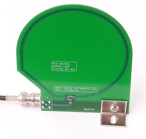
The Octal Data Receiver (ODR, part number A3027) is a receiver for use with our Subcutaneous Transmitters. The ODR provides eight independent antenna inputs for eight separate receiving antennas. We connect the antennas to the BNC sockets along the back of the enclosure with 50-Ω coaxial cables. The antennas are typically 915-MHz Damped Loop Antennas (A3015A). The ODR also provides four general-purpose digital signals on the front panel that we can configure for particular experiments.


Figure: Octal Data Receiver (A3027D), Front View.

The top row of fifteen LEDs show us transmitter activity. Activity on any channel number with remainder one (1) when divided by sixteen (16) will contribute to the brightness of the channel one (1) activity light. The channel seven (7) activity light is for channel numbers with remainder seven (7) when divided by sixteen (16). The fifteenth channel activity light is blue, for the auxiliary channels, which are those with remainder fifteen (15). The bottom row of eight LEDs tell us the activity on each of the eight antenna inputs. The two green lights indicate power is on. The yellow light is UPLOAD to the LWDAQ Driver. The red light is EMPTY message buffer. These two lights shine together when the LWDAQ is reading out messages as they are received by the ODR. The red switch is hardware RESET. The red light beside it is the RESET indicator. The brown and black switches, with their neighboring orange lamps, are the display function switches, SHOW and HIDE. When we press SHOW, all activity lights turn on. When we press HIDE, the activity lights toggle between being disabled and enabled. We disable the lights to reduce the current consumption of the ODR, which permits us to connect two ODRs to one LWDAQ Driver (A2071E).


Figure: Octal Data Receiver (A3027B) Inside View.

With its eight antennas, the ODR can pick up multiple copies of each transmitter message. The ODR eliminates almost all such duplicates before it stores them to its message buffer. Some duplicates remain. These are eliminated by the Receiver Instrument as soon as it receives the data from the ODR.


Figure: Schematic of SCT System with Octal Data Receiver. In this example, we are recording from thirty mice in six cages within an IVC rack.

The following assembly versions exist. For each, we give the minimum firmware version used to program the circuit's logic chips. The firmware version is available in the last byte of every clock message retrieved from the ODR, as it is with the older A3018. In order to distinguish the Octal Data Receiver (A3027) from the earlier Data Receiver (A3018), we add 30 to the ODR firmware version to create the number in the final byte of the clock message. When the ODR firmware version is 4, the last byte of the clock message will be 34. You can determine the firmware version of your ODR by setting show_messages to 1 in the Neurplayer's configuration panel. When you play back an interval, the firmware version number will be printed.

Assembly
Version
Description
A First prototype, no display board, no enclosure. 2
B Second prototype, hand-written labels. 3
C First production version, with hide and show buttons, printed labels. 4+
D Increased demodulator gain, otherwise as A3027C. 4+
E Stabilized intermediate frequency amplifier, dramatic performance improvement. 4+
Table: Versions of the A3027. For more details, see Modifications.

We describe the firmware versions below. Starting with firmware version nine (9), the A3027 supports communication with Animal Location Trackers (A3032). Starting with firmware version ten (11), the A3027 supports channel numbers 1-222 rather than the original 1-14. The Set Select Register on the A3027 permits the Receiver Instrument to configure the A3027 to record from only one transmitter set or from all of them.

Design

S3027_1: Amplifiers and Demodulators (Values as A3027D).
S3027E_1: Amplifiers and Demodulators (Values as A3027E).
S3027_2: Local Oscillator (Values as A3027D).
S3027_3: Power Supplies (Values as A3027E).
S3027E_3: Power Supplies (Values as A3027E).
S3027_4: Message Control.
S3027_5: Digital Input-Output.
S3027_6: Display Lamps.
Firmware: Logic code and compiled programs.
A3027D.ods: BOM and Pick-and-Place for A3027D.
A3027E.ods: BOM and Pick-and-Place for A3027E.
A3027D.pdf: Component map for A3027D.
A302701C: Gerber files and drawing fof main circuit board version C.
A302701C_Top: Top view of A302701C.
A302701C_Bottom: Bottom view of A302701C.
A302701D: Gerber files and drawing of main circuit board version D.
A302701D_Top: Top view of A302701D Main Board.
A302701D_Bottom: Bottom view of A302701D Main Board.
A302702A: Gerber and drawing files for display circuit board version A.
A302702A_Top: Top view of A302702A Display Board.
A302702A_Bottom: Bottom view of A302702A Display Board.

Operation

We control the Octal Data Receiver (ODR) through its LWDAQ interface, and read out the telemetry data through the same interface. The LWDAQ interface is the RJ-45 socket on the back of the ODR enclosure. This RJ-45 socket is not for Ethernet, but for a LWDAQ cable connecting the ODR to the driver. The driver can send sixteen-bit LWDAQ commands to the ODR, and it can read consecutive bytes from the ODR data buffer. The following table gives the ODR's allocation of LWDAQ command bits.

DC16DC15DC14DC13DC12DC11 DC10DC9DC8DC7DC6DC5 DC4DC3DC2DC1
R7R6R5R4R3R2 R1R0WAKELBXDTX XXISTSRESET
Table: Command Bit Allocation of the A3027.

The WAKE bit is reserved for LWDAQ, but serves no function on the ODR. The LB (loop-back) bit sets up the ODR's LWDAQ interface for a measurement of the total propagation delay from the driver to the ODR and back again. We use the loop-back function when looking for problems with the LWDAQ communication. The DTX (data transmit) bit directs the ODR to transmit the next byte from its data buffer when it receives a falling edge on the logic signal from the driver. The RESET bit resets the storage and readout memory addresses and many other internal state machines. It's the bit we write to from the Receiver Instrument to reset the data receiver. The ISTS (instant sample transmission select) bit is available in most, but not all, firmware versions. When we set ISTS, the upper bits R0..R7 represent a seven-bit channel number that the A3027 will match for immediate sample transmission on one of the general-purpose digital outputs.

Antennas

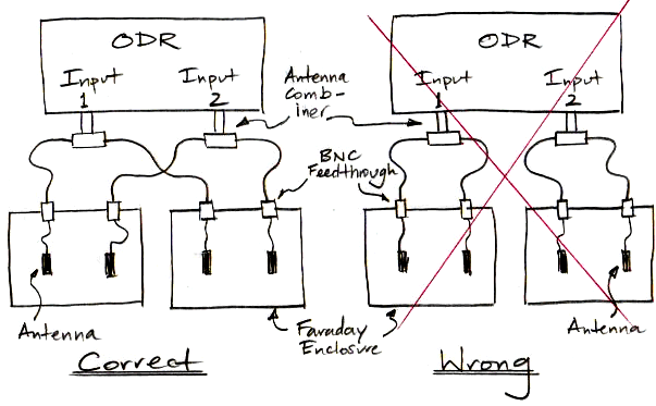
[22-MAR-21] We ship the ODR with eight 2.4-m RG58/U coaxial cables and eight 915-MHz Loop Antennas (A3015C). This antenna will stand upright on the floor of a faraday enclosure or on the surface of a shelf. We can remove its support brackets and strap it to the the structure of an IVC rack. The antennas will almost always be deployed within a Faraday enclosure, and we will carry the antenna signal to the ODR with two coaxial cables and a feedthrough connector.


Figure: Loop Antenna, A3015C, for use with ODR (A3027) Antenna Inputs. This antenna has a stabilizing 3-dB attenuator built in, to stop resonance in the cable between the antenna and the amplifier input.

The purpose of our Faraday enclosures is to isolate the receiving antenna from ambient microwave interference. If we run a coaxial antenna cable out of a Faraday enclosure without connecting its shield to the enclosure wall as it leaves, the cable becomes a conduit for microwave interference to enter the enclosure. Whenver we bring antenna signals out of an enclosure, we connect the antenna cable to a feedthrough in the enclosure wall, and then connect this feedthrough to the ODR with another coaxial cable. We have a variety of coaxial feedthroughs available, see here. Some are connectors mounted in the back walls of our bench-top Faraday enclosures, others are circuit boards we tape to the floor of our canopy enclosures.

The ODR provides eight independent antenna inputs so as to permit robust reception from moving subcutaneous transmitters. In order for the loop antennas to be independent in their reception of radio-frequency waves, we must place them at least 30 cm apart, which is one wavelength of 915 MHz in air. When we arrange antennas in a Faraday enclosure, we should make sure they are at least 5 cm from the conducting walls of the enclosure as well as separated by at least 30 cm. If the antennas are too close to the conducting walls, they stop working. If they are too close to one another, they receive the same signal, and so do not provide the independent reception that permits us to increase overall reception from many animals to ≥98%. The figure below is an example of an effective antenna arrangement.


Figure: An Effective Antenna Arrangement in an FE3A Faraday Enclosure. All antennas are at least 5 cm from the enclosure walls. Try to keep the antennas separated by 30 cm or more. The four coaxial cables should connect to separate antenna inputs on your ODR.

We can increase the operating area of our recording system by connecting multiple antennas to each ODR antenna input. Two antennas connected to the same antenna input will provide additional operating range provided the two antennas are in separate Faraday enclosures, or are least 60 cm apart (two wavelengths of 915 MHz). One way to connect multiple antennas to a single antenna input is with passive power combiners. The ZAPD-1 is a two-way power combiner that will keep the two antennas isolated from one another. The ZB4PD1-2000 allows us to connect four antennas with mutual isolation. Or we can connect two antennas with a BNC T-junction, like this one, and accept that the signal on one antenna will be carried to the other antenna. A BNC T costs about $5 and is readily available, while the two-way isolating combiner is $50 and is a speciality radio-frequency item. We recommend the BNC T as the simplest power combiner.


Figure: Correct and Wrong Way to Use Antenna Combiners. The combiner can be a "BNC T" adaptor.

When combining antenna signals, we must ensure that combined antennas are far apart from one another, or in separate Faraday enclosures. When arranging antennas in an IVC rack, we can use two Eight-to-Four Coaxial Feedthroughs (A3039C) to connect sixteen antennas to an ODR and so provide one antenna on either side of twelve animal cages. We make sure that each pair of antennas connected to each ODR antenna input is a pair that is separated by at least 60 cm in the rack. When arranging sixteen antennas among four Faraday enclosures, we make sure that none of the four antennas in each enclosure share an ODR antenna input with any other antenna in the same Faraday enclosure.

[25-SEP-15] We set up four antennas in our FE4A isolation chamber, one at the center of each wall, on the floor. We place a self-propelled ball with an A3028E attached to it on the floor, so that the ball moves and rotates the transmitter at random about the enclosure floor. We connect the four antennas to an A3027D in various ways. When we connect the antennas in pairs, we make sure that each corner of the enclosure has one antenna from each pair. We measure reception in one-minute periods, repeating the measurement several times for some configurations, in order to account for the dramatic variation in interference power in our office.


Figure: Reception from Moving Transmitter for Various Connections of Four Antennas. Separating lines indicate the passage of an hour or more between series of measurements. Local interference varies by two orders of magnitude on the timescale of one hour.

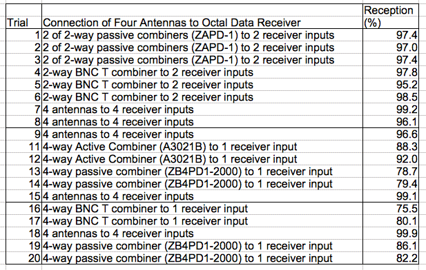
We see no significant difference between the $50 passive two-way combiner and the $5 BNC-T two-way connector in tests 1-8. The $100 passive four-way combiner, however, gives slightly better performance than a BNC-T four-way combiner. The BNC-T four-way combiner includes two cables as well as three BNC-T connectors.

[01-MAR-16] Reception from a subcutaneous transmitter varies dramatically with the relative orientation of the transmit and receive antennas. The axis of the transmitting antenna is the line bisecting the antenna loop and the transmitter body. When this axis is parallel to the plane containing the receiving loop antenna, we receive ten to a hundred times less power than when the axis is perpendicular to the receiving loop. If we have two antennas available to pick up signals from within one animal cage, we will do better to place the two loops perpendicular to one another. If we have three antennas that are mutually perpendicular, there is no orientation of the transmitter that will place its antenna axis perpendicular to all three receive antennas.

In practice, the reflecting walls of faraday enclosures and isolation chambers rotate the radio waves emitted by our subcutaneous transmitters, so that two antennas with parallel faces, but in different places, will receive the signal from a particular transmitter with a different orientation. Thus, if we keep two parallel antennas 30 cm apart, the chances of the signal received from the transmitter being unfavorably oriented with respect to both antennas is reduce. Nevertheless, we recommend that your antenna arrangement provide perpendicular antennas to make more certain of robust reception.

Local Oscillator

[02-APR-16] The local oscillator (LO), shown in S3027_2, generates a sinusoidal waveform of 866±1 MHz MHz that the A3027 uses to down-shift its antenna signals from 900-930 MHz to 34-64 MHz. The oscillator is based upon that of the A3016SO. We have an ERA-3SM amplifier, U1, whose output is fed back to its input through a 4-way splitter, a 6-dB attenuator, a delay line, and an 866-MHz SAW filter. Thermal noise is amplified by U1. Noise in the pass-band of the SAW filter arrives back at the input and is amplified again. A sustained oscillation develops at a frequency for which the net phase delay around the loop is 360°. The total distance the wave travels around this loop is roughly 134 mm, including the distance traveled through the components. According to our observations, with the ERA-3SM amplifier and a B3563 filter, we should get oscillation at around 865 MHz, and we find we get 866±1 MHz.

The SAW filter we used from 2013-2019 in the A3027A through A3027E is the B3563 with nominal center-frequency 864 MHz. We observed when working with our A3020SO that the B3563 supported oscillation at 865 MHz when combined with the phase shift of a 100-mm delay line and an ERA-3SM amplifier. The delay line is a way of introducing a known phase shift. We found that the phase shift of a SAW filter varies dramatically in its pass-band when we worked with our A3014SO. Thus we can tune our SAW oscillator by picking the correct delay line length.

The A3027 must provide a local oscillator for eight separate mixer. So we split it into four equal parts. One part goes back to the input of U1. One part we take through an attenuator to a BNC socket so we can measure the LO frequency. The other two parts we amplify with U2 and U3 and split into four parts each. The eight LO signals are nominally +6.6 dBm each, which is sufficient to drive the ADE-2ASK mixer used in the A3027 demodulating amplifier. We transport the LO signal with coplanar waveguides. We first used the coplanar waveguide in the Active Antenna Combiner (A3021B). The A3027 circuit board provides four copper layers. To build the waveguides, we clear the second copper layer, which is elsewhere the ground plane, and allow occasional power and low frequency tracks on the third layer. The bottom layer is the ground plane. The top layer is ground plane except where the curving signal traces run through it. The traces are 50-mil wide with a 7-mil gap to the ground plane on either side. The nominal trace impedance is 50 Ω. Phase delay is around 1.8°/mm. The distinctive curving tracks of the waveguides carry the LO power across the circuit board to the eight mixers of the demodulating amplifiers.

The J1 socket provides us with a convenient means to measure the LO power and frequency. In three separate A3027s, we measure +4 dBm and 866 MHz at J1. The four-way splitter (L4) and attenuator (R2) between U1 and J1 introduce a loss of 13 dB, so we believe U1 is producing 17 dBm. The input to L1, the SAW filter, is 4 dBm, which is a above its maximum power rating of 0 dBm. The inputs of U2 and U3 see 10 dBm, and we assume they produce 17 dBm also. Our LO1-LO8 signals for the eight antenna amplifiers will be roughly 11 dBm.

Demodulating Amplifier

[02-APR-16] The Demodulating Amplifier of the A3027E is shown in S3027_1. The circuit is similar to that of the A3017, except that we now use coplanar waveguides with ground planes to carry the RF signals before they are down-shifted. The demodulating amplifier circuit is repeated eight times, for n from 1 to 8, so as to provide eight antenna inputs.

At the intput of the amplifier, we connect an antenna. The antenna's all-frequency signal (AFn) is amplified by Un01, ERA-3SM, which provides ≈20 dB gain from 0.1-3 GHz. The amplified AFn passes through band-pass filter Ln03, B3588, which selects 900-930 MHz. The radio-frequency signal (RFn) output of the filter is amplified by Un02, ERA-3SM, and passes into mixer Ln04, ADE-2ASK, where it is multiplied by local oscillator signal LOn, which is 866±1 MHz. The mixer output is dominated by two components: the RFn signal downshifted by the LO frequency, and the RFn signal upshifted by the LO frequency. These two components occupy frequency ranges 34-64 MHz and 1766-1796 MHz respectively. The mixer output passes through low-pass filter Ln05, which passes frequencies 0-65 MHz, and so extracts the downshifted component of the mixer output, to produce the intermiediate frequency signal (IFn) in the range 34-64 MHz.

We amplify the IFn signal with a limiting amplifier made of three OPA699 op-amps. These op-amps limit their output to lie in the range VLB = 1.8 V to VLT = 3.2 V. We power the IF amplifier with a single +5 V so as to reduce power consumption. We use VCOM = 2.5 V as our signal ground. The VLB, VLT, and VCOM voltages generators are shown here. We couple the IF signal into each amplifier with 100 pF and 1.0 kΩ so as to provide a lower corner frquency of 1.6 MHz. When the corner frequency is below 100 kHz, the IF amplifier and the VLB, VLT, and VCOM generators can together sustain oscillate at a few tens of kilohertz. The limiting amplifier provides a total gain of around 65 dB, with output amplitude limited to 1.4 Vpp. The amplified IFn emerges as IFLn.

The IFLn signal passes through a 100-Ω resistor and a tank circuit made of a 100 nH inductor and a 47-pF capacitor. Depending upon the exact value of the inductor, we may add 10 pF to the capacitor to ensure the resonant frequency of the tank circuit is 930±3 MHz. The tank circuit takes the constant-amplitude, frequency-modulated IFLn signal and gives it an amplitude that increases with frequency from 900-930 MHz (Fn). We pass F into an amplifying demodulator made of diodes and op-amps. The rusult is the demodulated signal (Dn). The plots below show how D varies with frequency of the RF input.


Figure: Demodulated Output (Top, 500 mV/div) versus Frequency for One Antenna Input on the Octal Data Receiver (A3027A). Left −32 dBm sweep, right −80 dBm sweep. Bottom trace is the TUNE input to our Modulating Transmitter (A3014MT) Serial Number 1, see here for calibration. The left vertical line marks 900 MHz and the right is 930 MHz.

We obtained the above traces in the absence of significant local interference. In a city, we can expect a −80 dBm sweep to be overwhelmed by interference penetrating our A3027 enclosure, and expect our −73 dBm trace to look like the one on the right.

Discriminator

The output of the demodulator, D, passes through the discriminator filter to become the comparator signal C. The discriminator filter consists of Cn17, Cn18, Cn19, Rn20 and Rn21, as shown S3027_1. The filter combines a low-pass filter of 100 pF and 135 Ω with a high-pass filter of 200 pF and 540 Ω. Its step response is as shown below.


Figure: Step Response of Discriminator.

The discriminator filter extracts signals of average value zero and modulated at approximately 5 MHz from D. The modulation signal generated by reception of a subcutaneous transmitter message consists of transitions from one level every 100 ns or 200 ns. The step response decays slowly enough that 200-ns steps will be preserved adequately for discrimination, but longer HI or LO periods will be attenuated. In particular, the average value of the demodulated signal will be subtracted, so that it is only transitions in D that will be passed to the comparator. Steps shorter than 10 ns will also be attenuated, which reduces transitions caused by noise, and so reduces the bad message rate in the receiver.

The filter output passes into a comparator, and so becomes a sequence of logic levels, Qn. The combination of the discriminator filter and the discriminator comparator are the discriminator. The filter is based upon that of our Data Receiver (A3018D). We have increased the resistors by a factor of ten and reduced the capacitors by a factor of ten so as to increase the network's impedance by a factor of ten while leaving its step response the same.

Robustness of Reception

With eight independent antennas, the A3027 is supposed to provide far more opportunities for a transmitter message to be received and decoded. Transmitter messages are received correctly when their power is more than ten times the power of the ambient radio-frequency interference in the 900-930 MHz band. Otherwise, the interference dominates.

[30-AUG-13] We place two A3015B loop antennas beside a piece of letter paper on a table. The antennas are on adjacent sides of the paper. We connect one antenna to our A3027 and move an A3019D around over the paper in our hand at random. Reception is 24% over one minute. If the chance of a message being lost is 75%, the chance of it being lost by two independent antennas is 50%. With two antennas we expect 50% reception. We connect the second antenna and repeat the measurements. Reception is 74%.

[20-SEP-13] We set up three A3015B loop antennas all in a row, separated by 30 cm, with their loops co-axial. Our ambient interference power is −49 dBm as measured by our A3008B spectrometer. We take an A3019D transmitter in hand, with its antenna exposed to air and move it at random in the 30 cm cube between the left and center antennas for one minute. Reception is 100.0%. We disconnect the right-side antenna. Reception drops to 98.2%. We disconnect the left-side antenna. Reception drops to 96.6%. We repeat these three measurements, but holding the transmitter entirely enclosed in our hand, so the antenna is enclosed in human body tissue at least 2 cm deep. We obtain 94.4%, 84.6%, and 53.8%.

Let us suppose that the chance of a message failing to arrive at an antenna is independent for the three antennas. In that case, the chance of losing a message is 3.4% for antenna in air and 46.2% for antenna in hand. We would then expect reception for two antennas to be 99.9% and 78.7% respectively. We see 98.2% and 84.6%. For three antennas we would expect 100.0% and 91.9%. We see 100.0% and 94.4%. It appears that the chance of one antenna missing a message is slightly lower if another antenna is missing the same message at the same time, so an assumption of independence gives us a conservative estimate of the benefit of multiple antennas.

[31-OCT-13] At ION, we set up an Octal Data Receiver and plug in four antennas. We arrange them as if they were on the shelves of an IVC rack, with no enclosure or absorbers around about. We measure reception as if in a cage between them by holding the entire transmitter in our fist and rotating at random for ten seconds, while watching reception in the Receiver Instrument. With one antenna we get 30±10% reception, two give us 60±10%, three gives us 90±5%, and four gives is 97±3%.

[31-DEC-13] The Octal Data Receiver, like the Data Receiver (A3018), requires that transmit clock period of the messages it receives be close to 200 ns, for 5 MBPS. Today we used a batch of A3028s to obtain the following graph of reception efficiency versus transmit clock period. In all cases we ensured that the mark-space ratio was 48-50%.


Figure: Reception versus Transmit Clock Period. Reception is from two-channel transmitters, so we have two graphs, one for the first channels and another for the second channels.

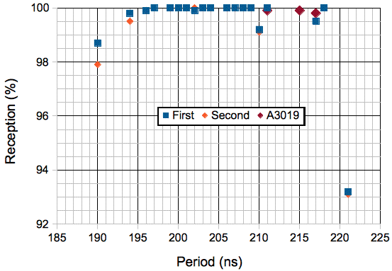
Reception works well for clock periods 195-218 ns, but poorly outside that range.

[10-MAR-14] We set up eight antennas in an IVC rack at ION and measure reception with and without the walls of a radio-frequency isolation chamber around the rack. Without the isolating walls, reception is adequate in the cages well-covered by antennas. With the isolating walls, reception is 100.0% everywhere in the rack. For photograph and more details see Performance of Chamber for IVC Rack.

[08-OCT-14] We set up a 1.2 m × 0.6 m isolation chamber on our concrete basement office floor with a sheet of reflecting steel mesh fabric on top. We attach an A3019D transmitter to a self-propelled ball and allow the ball to move the transmitter at random across the floor of the enclosure. Click on the figure below for a video of the ball in action.


Figure: Radio Frequency Isolation Chamber and Self-Propelled Ball with Transmitter.

We record for one minute within the chamber with between 1 and 4 antennas, and with the roof on and off in the case of 4 antennas. The graph below shows how reception varied during a minute under each arrangement.


Figure: Reception During Sixty Seconds for Various Arrangements of Antennas and Roof. For each plot we give the number of active antennas and whether or not the roof is on or off.

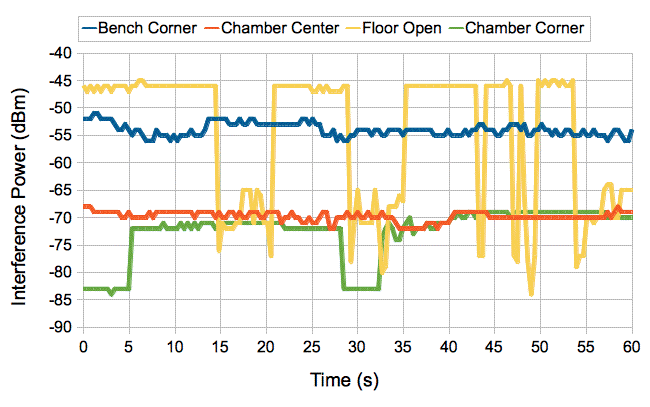
The average reception during the one minute is for 4-ON 99.9%, 4-OFF 86.8%, 3-ON 98.8%, 2-ON 96.5%, 1-ON 82.9%, and 4-ON repeated 99.7%. Our intermittent local Ê is particularly powerful. As shown here, the power outside our chamber reaches −45 dBm, while within the chamber we get no more than −70 dBm. We see today that the roof of the isolation chamber is necessary to ensure robust reception, which we define as ≥95%. We need two or more antennas.

[07-JUN-17] We have a ten-minute recording of a transmitter attached to a self-propelled ball rolling around in a box with two receiving antennas in an FE2F enclosure. We obtain the following loss of signal.


Figure: Reception from Transmitter on Self-Propelled Ball in FE2F Enclosure with Two Antennas.

[09-JUN-17] We have 10 of A3028L dual-channel 1024 SPS transmitters, channel numbers in the range 71-94. We turn them all on and place them in water within a faraday enclosure with two antennas connected to an A3027E. The total sample rate is 20 kSPS. We plot reception versus time in one-second intervals for the channels with the best and worst reception.


Figure: Reception from Ten Dual-Channel 1024 SPS Transmitters with Two Antennas. We plot the best and worste channels. Their average reception is 96% and 77% respectively.

Each channel has eighteen others with which it can collide (transmitters don't collide with themselves). We discuss collions in detail here. Each transmission is 7 μs, so the likelyhood of a given sample colliding with another is, on average, 7 μs × 2 × 18 × 1024 ÷ 1E6 = 25%. With one antenna we expect an average 75% reception. We observe an average of 87% with two antennas for all channels combined, and a minimum average of 77% for any one channel.

[25-OCT-23] We have four SCTs in boxes with connectors, each with a different center frequency. We have measured their power output. With attenuators, we can vary the SCT signal power we deliver to a combiner, in which we combine the SCT signal with a constant-frequency interference signal that we adjust to the center frequency of the SCT signal. For SCT signals −47 dBm to −5 dBm we measure the maximum interference power for which we can still obtain 90% SCT reception. We plot the ratio of interference power to signal power. This ratio is our interference tolerance.


Figure: Interference Tolerance of the Octal Data Receiver (A3027E). For four center frequencies, and a range of signal powers, we give the maximum ratio of constant-frequency interference power to signal power for which we obtain 90% reception. (By Nathan Sayer)

The interference tolerance of the ODR is between −10 and −5 dBm for the range of signal powers we are likely to see on a telemetry antenna.

Power Supplies

[25-APR-17] We measure the current consumption of five A3027Es and get 240-243 mA from ±15V and 222-230 mA from +5 V when the circuits are idle. There are no antenna or activity lights illuminated. Given that the power supplies of the LWDAQ Driver (A2071E) are rated at 500 mA at ±15V and 2000 mA at +5V we see that a single LWDAQ driver should, in theory, be able to support two A3027E ODRs. When we press the SHOW button to turn on all the white LEDs, current consumption increases to 330 mA, at which point we cannot connect two A3027s to one LWDAQ Driver (A2071E). If you want to connect two A3027s, press the HIDE button to disable the indicator lights, and current consumption will be reduced.

[25-APR-14] The A3027 uses only +5 V and +3.3 V power. The +5 V runs the Local Oscillator, the Radio-Frequency Amplifiers, the Intermediate Frequency Amplifiers, and Demodulators for the eight antenna inputs, as well as the white and blue indicator lamps on the front panel. This +5 V we obtain with a CC10-2405SR-E 5-V isolated output DC-DC converter, L10, from the LWDAQ ±15 V power supply. The logic runs off +3.3 V. This voltage we obtain with an LTC3404 buck regulator, U7, with a 10-μH inductor, L9, from the LWDAQ +5 V power supply.


Figure: Current Consumption of the A3027 as Measured by LWDAQ Power Monitors.

The difference between the +15V and −15V current is due to a scaling error in the current measurement made with the LWDAQ power monitors. When we plug a second A3027C into one A2037E driver, the ±15-V power supplies turn off. When the A3027C starts up, it's light flash and it draws a total of 341 mA. This adds to the first A3027C's 255 mA to make almost 600 mA. The LWDAQ ±15-V current limit is 500 mA. With the white indicator lamps turned off, the A3027C to consumes 250 mA from 30 V. The L10 converter is 86% efficient, so it appears that the A3027 is drawing around 1.2 A from its +5-V power supply, which is what we estimate from looking at the typical current consumption of the amplifier and local oscillator components.

Message Control

[27-JAN-17] The A3027 message control consists of a Message Detector, Message Router, and Message Memory. Messages are detected, selected, stored in memory and uploaded to the LWDAQ driver when requested by the data acquisition software.

The Message Detector is U16, a 512-gate programmable logic chip. The outputs of all eight Demodulating Amplifiers are connected to the Message Detector, which provides eight independent message decoding circuits to identify SCT messages in the random sequence of bits generated by noise, interference, and SCT signals in each Demodulating Amplifier. The Message Detector uses a temperature-compensated 32.768 kHz oscillator, U13, to provide a timestamp for message. It eliminates almost all duplicate messages detected by its multiple antennas. For details of how it works, see the P302702Axx.abl and P302702Axx_Decoder.abl files, where xx is the version number. The Message Detector functions use up 90% of the logic available in U15.

The Message Router is U15, another 512-gate programmable logic chip. It reads messages one byte at a time from the Message Detector and stores them in RAM at its storage address. When it receives a data strobe from the LWDAQ Driver, it fetches a byte from RAM at its transmit address. For details of how it works, see the P302701Axx.abl and P302702Axx_Indicator.abl files, where xx is the version number. The Message Router functions use only 30% of the logic available in U15.

Memory

[10-SEP-13] The A302701A layout provides U14, a 512 KByte, 10-ns static RAM. This works fine, and is identical to the memory used by the A3018. The Message Router has three hundred spare logic gates, which is enough to build an eight-bit microprocessor with a hardware multiplier (see ISL Conceptual Design). If we were to implement a microprocessor in the Message Router, we had best provide some non-volatile memory for an operating system. Thus we add a serial FRAM (Ferromagnetic Random Access Memory) in an SOP-8 package to the A302701B layout. The FM25V02 from Cypress provides 32 KBytes of 40-MHz non-volatile RAM.

Digital Input-Output

The A3027 provides two bi-directional low-voltage differential logic signals (LVDS) and two bi-directional 3.3-V single-ended logic signals. The S3027_5 schematic shows all four logic signals and their connectors. The LVDS signals are Y1 and Y2. They are available on the front panel of the A3027 on two USBA plugs. These plugs also provide 5-V power for auxiliary circuits. The single-ended signals are X1 and X2. They are available on the front panel on two BNC sockets. There is a 1-kΩ resistor in series with X1 and X2, and diode clamps, to protect the A3027 logic chips from electrostatic discharge and external over-voltages.

The A3027 firmware determines the behavior of each signal. We describe the behavior of the inputs and outputs in below.

Firmware Versions

The A3027 firmware version determines the behavior of the inputs and outputs, as well as correcting bugs in the operation of the logic, and adding features such as increasing the range of channel numbers from 0-15 to 0-255. To re-program your firwmare, see Firmware Reprogramming. For an example of a program that uses the A3027 logic outputs to control other hardware, consider the Slow Pulse Generator.

Firmware X1 X2 Y1 Y2 Features
4 Antenna One Detecting Unused Input Message Detector Code Unused Input None
5 Antenna One Detecting Immediate Sample Transmission Message Detector Code Unused Input None
6 User Logic Output User Logic Output Message Detector Code Immediate Sample Transmission None
7 User-Enabled Pulses, 1 ms at 24.6 Hz. User Logic Output Message Detector Code Immediate Sample Transmission None
8 User Logic Output Immediate Sample Transmission Prototype Message Notification Prototype Message Notification None
9 User Logic Output Immediate Sample Transmission Message Notificaion for Location Trackers Message Notification for Location Trackers None
10 User Logic Output Immediate Sample Transmission Message Notificaion for Location Trackers Message Notification for Location Trackers Support for SCT set numbers, default Set 0,
no duplicate rejection.
11 User Logic Output Immediate Sample Transmission Message Notificaion for Location Trackers Message Notification for Location Trackers Support for SCT channels 1-223, default Set 0,
no duplicate rejection.
12 User Logic Output Immediate Sample Transmission Message Notificaion for Location Trackers Message Notification for Location Trackers Support for SCT channels 1-223, default Set 0,
with duplicate rejection.
13 User Logic Output Immediate Sample Transmission Message Notificaion for Location Trackers Message Notification for Location Trackers Support for SCT channels 1-223, default all sets,
with duplicate rejection.
Table: Configuration of Digital Input-Outputs in Firmware Versions. You can determine the firmware version of your A3027 by looking at the Receiver Instrument panel, where there is a firmware version display box. The firmware version number will be displayed with 30 added to it to distinguish the A3027 firmware versions from those of the earlier A3018 recorder.

Firmware Version 4: The X1 output is Antenna One Detecting. Any time Antenna One receives something that starts to look like an SCT message, X1 goes HI. The photograph below shows X1 when we are receiving perfectly from three transmitters that are not colliding.


Figure: Antenna One Detecting Output on X1. We have a sharp rising edge for X1 on the A3027 circuit board, and a slower rising edge at the end of a 1-m coaxial cable with a 50-pF terminating capacitance.

We use the X1 signal to trigger on SCT transmissions so we can examine signals inside the A3027 and watch the transmit bits as they are amplified and demodulated. The X1 signal is asserted after five synchronizing edges are received from the transmitter. The 6.1 μs detection time is the remaining 31 bits transmitted by these SCTs, at a nominal 200 ns per bit, gives 6.2 μs. The actual bit time varies from one transmitter to the next, which is why there are three falling edge locations in the photograph.

Firmware Version 5: We configure the A3027 for Immediate Sample Transmission. By transmitting a command through the LWDAQ to the A3027 we select one channel number for immediate transmission as a sixteen-bit serial word on X2. A LWDAQ command is itself a sixteen-bit number. We can send individual commands to the A3027 with the Diagnostic Instrument. The sixteen-bit hexadecimal command 0n02 instructs the A3027 to transmit all samples it receives from channel number n. When the A3027 powers up, the selected channel number is zero, so the A3027 transmits the samples of channel zero, which is the timestamp channel. The transmitted samples start at zero and increase to 65535 at 128 SPS. If we turn on an A3028A dual-channel 512 SPS transmitter using channels 1 and 2, we can select the first channel for immediate transmission with command 0102. If we want to select channel number 141, we must translate 141 into hexadecimal, and enter 8D02. The channel selection will remain in place until we send another command to change its value, or we press the front-panel hardware reset button, or we cycle the power.

The speed with which we can transmit the sixteen-bit serial word is limited by the length of the coaxial cable we use to carry the signal to our external logic, and the terminating capacitance at the end of the cable. The photograph below shows a 333 kHz clock on X2 with a 2.6-m RG58C cable and a 50-pF terminating capacitor.


Figure: Rise Time of X2 with 2.6-m Coaxial Cable and 47 pF Load. The sharp rising edge is X2 on the A3027 circuit board, after the 1k0 series resistor (R21). The longer rising edge is X2 at the far end of the cable.

The flickering in the rising and falling edges are periodic steps in the edges with period 28 ns. Our coaxial cable has propagation delay 4.0 ns/ft and length 2.6 m. The signal takes 10.4 ns to reach the far end of the cable, where it is reflected, and 10.4 ns to come back. When we shorten the cable to 107 cm, the period of the steps drops to 11 ns. The immediate sample transmission proceeds at 4 μs per bit, so as to give plenty of time for the signal at the other end of a 2.6-m cable to settle for each bit. The photograph below shows the transmission of timestamp samples.


Figure: Immediate Sample Transmission on X1 at the End of 2.6-m Cable. Here we show transmission of channel zero, the timestamp channel. The transmission begins with a LO bit (far left), then the sixteen sample bits, most significant first and least significant last. The rightmost, least significant, bits appear to have two values at once because they are changing state even as we take the photograph. The dots in the transitions are the steps in the rising edge caused by reflections.

The X2 output has a rest state of 3.3 V, or logic HI. To initiate serial transmission, it asserts a 0.0 V, or logic LO, for one 4-μs bit period. It proceeds from there to transmit the sample bits one at at time, from the most significant to the least significant.


Figure: Transmission Scatter Seen on X2 from a 512 SPS Transmitter.

If we expand the oscilloscope view, we start to see subsequent samples. The photograph above shows the subsequent sample transmissions when we select a 512 SPS transmitter. Transmitters have sample scatter, as we describe elsewhere. Thus the samples do not arrive at a uniform rate, but rather at an average rate of 512 SPS.

Firmware Version 6: We configure X1 and X2 to be digital outputs set by LWDAQ Commands. The Immediate Sample Transmission of Version 5 now goes to Y2 and the Antenna One receiving signal goes to Y1. To set X1 to 1, or 3.3 V output, we transmit command 0x0104 to the A3027C (the 0x is for hexadecimal notation). To clear X1 to 0, or 0.0 V, we transmit 0x0004. To set and clear X2 we transmit 0x0108 and 0x0008 respectively. We can transmit these commands with the Diagnostic Instrument, which we set up like this. We set the transmit command in hexadecimal notation and press Transmit to send the command to the Diagnostic Instrument's target device.

The following oscilloscope traces show X1 and X2 being switched by the Diagnostic Instrument. We enter two commands and the Diagnostic Instrument will transmit both of them sequentially.


Figure: Switching X1 and X2 with Firmware Version 6. Top trace is X1, bottom trace X2. We have transmit commands "0104 0108 000C" being sent repeatedly. The result is that X1 goes HI (3.3 V), then X2 goes HI, then both go LO.

Because the immediate sample transmission is now a low-voltage differential signaling (LVDS) output, it's transitions are a thousand times faster than when they emerged on X2.


Figure: Immediate Sample Transmission on Y2 in Firmware Version 6. The logic transitions now take nanoseconds rather than microseconds.

In future versions of the firmware, it will be possible to reduce the clock speed of the sample transmission, from the existing 4 μs to 50 ns.

Firmware Version 7: We configure X1 to produce 1-ms, 3.3-V pulses at 24.6 Hz when we write 0x0104 to the A3027, and a continuous 0 V when we write 0x0004. Thus we replace the HI of Firmware Version 6 with a sequence of pulses. We intend for these pulses to be used to trigger image capture by closed circuit television recorders. The Y2 output is Immediate Sample Transmission, controlled as in Firmware Version 6.

Firmware Version 8: A prototype of Firmware Version 9 in which the message notification worked poorly. Exists only in receiver P0245. We restore immediate sample transmission to X2.

Firmware Version 9: The differential outputs, Y1 and Y2, transmit message notifications. These are 36-bit serial words transmitted at 20 MBPS (50 ns per bit). There are three types of notification. The first is message incoming, which the A3027 transmits when one of its message decoders has received eight complete and correct bits of a twenty-four bit message. The second is clock message, which carries the value of the A3027's clock. The third is data message, which carries the channel number, contents and timestamp of a data message.


Figure: Message Notification on Y1/Y2. The bottom trace is the transmit bit output from an A3028A dual-channel transmitter. The top trace is the message notification signal sent out of Y1 and Y2.

In the figure above, we see the Y1/Y2 signal is by default HI (1). The message incoming notification takes place roughly half-way through the transmitter radio-frequency burst, following eleven start synch bits, a start bit, and eight data bits received. The notification is a serial transmission of the value 0xA, followed by all ones. When the message has been decoded, we have a message data notification, which begins with the value 0xC, followed by the eight-bit channel number, sixteen bits of data, and an eight-bit timestamp. Clock messages are transmitted in a similar way, starting with value 0xB, eight zeros for the clock channel number, the top sixteen bits of the timestamp, and then the A3027 firmware version number.

In order to guarantee that all clock messages stored by the A3027 are transmitted in the notification data stream, all message notifications and incoming notifications are suppressed for 30 μs before each clock message. The clock messages are saved every 7.8 ms, so we miss 0.3% of data messages in this way.

The Message Notifications are designed for use with the Animal Location Tracker (A3032A). The X1 output is set by a LWDAQ command. To set X1 to HI, or 3.3 V, transmit 0x0104. To clear X1 to LO, or 0.0 V, transmit 0x0004. The X2 output is Immediate Sample Transmission, as in Firmware Version 5.

Firmware Version 10: Adds support for set numbers. All SCTs belong to a transmitter set between 0 and 13. By default, FV10 responds only to channels 1-14. Starting with FV=10, we can write to a four-bit register on the A3027 to change the set number it records from. The Receiver Instrument in LWDAQ 8.4.5+ includes a parameter daq_set_number that the Receiver Instrument writes to the data receiver before every interval download. The FV=10 firmware introduces a four-bit register space sixteen registers long. The first register, address zero, controls X1. To set or clear X1 we write 0x0104 and 0x0004 to the A3027. To assign the value S to the Set Select Register, we write to the second register, address one, with 0x1s04, s is the hexadecimal representation of S. The remaining fourteen registers are available for future use. If we write value 0xF (decimal 15) to the Set Select Register, the A3027 will accept messages from all sets. If two transmitters have the same channel number, but different set numbers, their signals will be combined into the same channel. The X2 output is Immediate Sample Transmission, as in Firmware Version 5.

Firmware Version 11: Supports channel numbers 1-223 as described here. By default, FV11 responds only to channels 1-14. receives only from Identical to firmware version 10 except for two changes. The set number is always stored in the top four bits of the channel number. When all sets are being recorded, duplicates messages are not elimiated. If eight antennas receive the same message, eight copies will be stored. The Receiver Instrument in LWDAQ 8.4.9+ purges duplicatse as soon as it receives them, but they must still be downloaded. Immediate sample transmission as for FV = 5.

Firmware Version 12: Supports channel numbers 1-223 as described here. By default, FV12 responds only to channels 1-14. Duplicate reduction replaces duplicate elimination. We remove >99% of duplicates. The remaining duplicates are eliminated by the Receiver Instrument. The X2 output is Immediate Sample Transmission, as in Firmware Version 5.


Movie: How to Set and Clear Logic Output X1. In this 150-s video, we demonstrate how we can set and clear the 3.3-V logic output X1 using the LWDAQ Diagnostic Instrument. This procedure works on any A3027E with firmware version 8+.

Firmware Version 13: As Version 12, but corrected error in implementation of antenna activity lights and the default configuration is to detect all channel number sets, rather than only set zero. The X1 output is user logic output as in FV6. The X2 output is Immediate Sample Transmission, as in FV5. The Y1 and Y2 outputs are both dedicated to message notification for location trackers.

Firmware Reprogramming

[28-FEB-17] There are three programmable logic chips in the A3027 enclosure. The Message Router chip controls how transmitter messages are stored in memory and uploaded to the LWDAQ Driver. In firmware version xx, the Message Router logic is defined in source file P302701Axx.abl. We program the chip itself with compiled file P302701Axx.jed. The second logic chip is the Message Decoder, which controls how incoming bit sequences are received. The Message Decoder is defined by P302702Axx.abl and programmed by P302702Axx.jed. The third logic chip is the Display Controller, which we define with P302703Axx.abl and program with P302703Axx.jed. The Message Router and Message Decoder are both on the main circuit board inside the A3027 enclosure, and we program them with one operation. The Display Controller chip is on the circuit board behind the display lights, and we program it with its own operation. Most likely, you will not have to upgrade your display board firmware, so the only operation you need to perform to update your A3027 firmware is to re-program the Message Router and Message Decoder on the main circuit board.

The A3027 logic chips are manufactured by Lattice Semiconductor. To re-program them, you need the programming cable and software. The cable is described on-line here. The programming cable is available from DigiKey and RadioSpares. The Windows version of the programming software you can download here. There is a Linux version also, but we do not maintain a copy of the Linux version ourselves. There is no MacOS version. The programming cable comes with many wires and a single-row eight-way socket adaptor that you use to connect the wires called VCC, TDO, TDI, TMS, GND, and TCK to the circuit you want to re-program. The following movie shows you how to attach the wires to the adaptor.


Movie: How to Assemble the Terminating Connector of the Lattice Semiconductor Programming Cable.

In the programming software, select Help and search for "USB Driver". Follow instructions to install USB port drivers. If the program tells you the drivers are already installed, re-install them. Plug the programming cable into your computer when the installer asks you to do so. Install all versions of the USB driver. Restart the programming software. You are now ready to reprogram the logic chips. In the following movie, we reprogram the two logic chips on the main circuit board.


Movie: Overview of Firmware Reprogramming. Here we are using the older, ispVM version of the programming software.

The software procedure is slightly different for the newer version of the programming software. We demonstrate the newer procedure in the video below.


Movie: Using the Diamond Stand-Alone Programming Software.

If the software scans the A3027 firmware correctly, but fails to program the firmware afterwards, go into the programmer software settings and adjust the programmer configuration by clicking "continue download on error". We have had to make this adjustment on some virtual Windows machines. The programming will now proceed, but you will get a warning at the end. In our experience, the firmware will be loaded correctly into the A3027 despite the warnings.

The programming software takes JEDEC files as input. The following table provides links to the JEDEC files you need for various firmware versions. In order to show when you have to reprogram the Display Controller, we provide the earliest version of Display Controller firmware that is compatible with each overall firmware version number. Firmware versions 4-12, for example, all use the Display Controller firmware of Firmware Version 4. So if your existing firmeware version is 4 and you are upgrading to 12, you don't need to re-program the Display Controller on the display board.

Version Message
Router
Message
Detector
Display
Controller
4 P302701A04.jed P302702A04.jed P302703A04.jed
5 P302701A05.jed P302702A05.jed P302703A05.jed
6 P302701A06.jed P302702A06.jed P302703A06.jed
7 P302701A07.jed P302702A07.jed P302703A07.jed
8 P302701A08.jed P302702A08.jed P302703A08.jed
9 P302701A09.jed P302702A09.jed P302703A09.jed
10 P302701A10.jed P302702A10.jed P302703A10.jed
11 P302701A11.jed P302702A11.jed P302703A11.jed
12 P302701A12.jed P302702A12.jed P302703A12.jed
13 P302701A13.jed P302702A13.jed P302703A13.jed
Table: JEDEC Files for Firmware Versions. Click on the links to download the files. Save them to disk.

Determine the firmware version of your A3027 by looking at the Receiver Instrument panel, where there is a firmware version display box. The firmware version will be displayed with 30 added to it, so 42 is firmware version 12.

Once you have downloaded the JEDEC files you need, scan the programming connector on the A3027 with the programming cable using the Scan button in the programming software. A new window will open and you will see two logic chips listed in the programming cable window. By clicking on the file entry box next to each logic chip, you can associate each chip with a JEDEC file. The first chip listed is the Message Router, which takes the 01Axx.jed files and the second is the Message Decoder, which takes the 02Axx.jed files. Press Go and the programming begins. When it is done, unplug the cable and test the A3027. You can reprogram the firmware as often as you like.

Indicator Lamps

[29-AUG-13] We have added a Receive indicator to the A302701B printed circuit board, and implemented the code for it in the Message Detector.

[10-SEP-13] We do not have the Display Board (PCB will be A302702A) laid out or built yet, but we have tested the use of SCK to provide flashing lights in the UPLOAD indicator. The Message Detector generates an eight-bit code every time it stores a message, and transmits this code to the Message Router. The code contains the antenna that received the message and the channel number of the message. This code is transmitted regardless of whether or not the message is transferred to the Message Router. Thus duplicate messages are reported by their own codes, so that the display board will be able to indicate which antennas are picking up a signal.

[02-OCT-13] We complete the Display Board layout A302701A. It includes white LEDs to indicate reception on channels 1 through 14, and on antennas 1 through 8. We have a blue LED for reception on channel 15. We have various red, amber, and green LEDs for other signals, and three switches, including a reset switch.

[16-OCT-13] We have the antenna and channel indicator lamps turning on correctly with reception.

[24-OCT-13] We improve the control of the white channel and antenna amplifiers. The Message Detector indicates incoming messages by sending an eight-bit message detector code every time a message is received. These codes come in bursts a few microseconds long. Each message provokes a 60-μs flash 30-60 μs after it is received.

Modifications

A3027A: Original prototype, only three amplifiers loaded, A302901A printed circuit board. The A302701A PCB has many problems and is not used in any production version of the A3027.

A3027B: First fully-populated prototype with hand-written labels in metal enclosure. Used the A302801B printed circuit board. Was later modified to become an A3027C, so no A3027B exists.

A3027C: First production version of the A3027. The first five use the A302801B printed circuit board, which does not include capacitors Cn24, while capacitors Cn21 are not close enough to comparators Un07 to be effective, and the layout does not include resistors R52-R54, which suppress 10-kHz oscillations in the IF amplifiers. We corrected these problems by hand in all 5 of A3027C that use the A302801B.

A3027C, Blue Dot: We insert a 6-dB attenuator, R55, before the input of L1 to protect if from damage. Without this modification, the LO will degenerate over a period of a few weeks continuous running. The result is shown below.


Figure: The Blue Dot Modification. This modification is required by A3027Cs using the A302701B circuit board. Component R55, a 6-dB attenuator, is in the lower right of the photograph.

We performed the blue dot modification on all five A3028Cs made with the A302701B printed circuit board. Assemblies P0245, Q0134, Q0135, Q0318 (original serial number Q0136), and Q0137 started off as A3027Cs with the blue dot. The A302701C printed circuit board adds capacitors Cn24, moves capacitors Cn21, includes resistors R52-R54, and attenuator R55. The A3027C made with the A302301C printed circuit board has no blue dot on its serial number label. Assemblies Q0196 and Q0197 started off as A3027Cs.

A3027D: We replace 1.0-kΩ Rn15 and Rn18 with 330 Ω and 56-pF Cn14 with 47 pF, to increase the gain and shift up the peak demodulation frequency. The result is the A3027D, made with A302701C circuit boards. Assemblies Q0211, Q0138, Q0139, Q0144, Q0145, and Q0153 started off as A3027Ds.


Figure: Correct Orientation of J3 on the Main Board.

A3027E: We change Cn06, Cn08, and Cn11 to 100 pF in place of 10 nF, raising the corner frequency of our IF amplifier to 1.6 MHz from 16 kHz. It is no longer possible for oscillations of a few tens of kilohertz to develop in VTL, VTB, and VCOM, allowing us to set R52-R54 to 0 Ω, which greatly improves the stability of the demodulation for both strong and weak signals, and for high and low frequencies, as shown below.


Figure: Reception (%) versus Signal Power (dBm). A Comparison of the A3027D (Lines D), A3027E (Lines E), and A3018D (Line OLD) at Various Frequencies. Power 0 dBm is 1 mW, and −60 dBm is 1 nW. Each plot is for a different amplifier and transmit center frequency in Megahertz. The signal is −5 dBm directly from an un-encapsulated A3028E, and attenuated with coaxial attenuators.

The plot above shows the 20-dB improvement in sensitivity provided by the A3027E modification for frequencies 911 MHz and below, and 10-dB improvement at higher requencies. Reception for powerful signals is now 100% at all frequencies. When compared to the A3018D, the A3027E has 10 dB higher sensitivity at all frequencies. Even an A3018D with active antenna combiner, which provides 6 dB more sensitivity, is still 4 dB behind the A3027E.

We recall all existing A3027C and A3027D circuits for upgrade to A3027E. The upgraded A3027D is identical to a newly-made A3027E. When we upgrade an A3027C, we check reception at 923 MHz on all antenna inputs. If reception is less than 98% on any amplifier, we replace Cn14, which is 56 pF, with 47 pF. Thus the value of Cn14 varies. All resistors Rn15 and Rn18 remain 1.0 kΩ, rather than 330 Ω.

When we have the A3027E assembled, we load 39 pF for Cn14. Sometimes this value is perfect. Sometimes it is too low, and we add a small capacitor in parallel to tune the demodulator.

A3027E, Blue Dot: The A3027E with a blue dot on its serial number label has a microwave absorber glued to the underside of the lid. The absorber provides better isolation of the A3027E amplifiers from 902-928 MHz interference outside the enclosure. We see a dramatic reduction in the bad message rate caused by interference sources when we add the absorber.

Development

2013

[08-AUG-13] The RF amplifier gain from the A1 to IF1 is 27.3 dB of gain. The gain in amplifiers U101 and U102 combined is 27.3 + 3 (loss in B3588 filter) + 7 (loss in mixer) + 1 (loss in L105) = 38.3 dB. Each ERA-3SM amplifier is providing around 19 dB of gain, which is satisfactory.

The IF amplifier oscillates until we realize that we must decouple +5V and VCOM directly to 0V instead of decoupling +5V to VCOM. We increase the decoupling capacitors to 1.0 μF and add one at the base of L106 and R104. The amplifier is now stable and provides sensitivity down to −82 dBm at the antenna input. We expect thermal noise at the antenna input of −93 dBm in our 30-MHz bandwidth. With the +2.6 dB noise figure of the ERA-3SM we get −90 dBm. Thus we are able to detect our sweep within 8 dB of the expected noise.

[28-AUG-13] We take out an un-encapsulated A3013A and trigger on its modulation test point to watch the comparator output from our No1 demodulator. All looks well. We place this transmitter 10 cm in front of the A3018C antenna in our office. With 30 dB of attenuation in line with the antenna, reception drops to 50%. We repeat the experiment with our A3027A antenna and find that 42 dB of attenuation is required to drop reception to 50%. The A3018C with an Active Antenna Combiner (A3021B) is 6 dB more sensitive, so the remaining 6 dB improvement we hope is due to the superior performance of the A3027 amplifiers.

[29-AUG-13] We build two more amplifiers. Their gain is within 2 dB of the first. We set the tuning capacitor Cn14 to 60 pF, which we construct using two 5% 30-pF. With 100 nH, we expect a resonant frequency of 65 MHz, which will correspond to 865 + 65 = 930 MHz. In all three demodulators, we find the peak frequency lies within 2 MHz of 930 MHz.

[30-AUG-13] We turn off the duplicate removal in our Message Detector. We terminate A2 and A3 with 50 Ω and connect A1 to an antenna through an attenuator. We have an A3019D 10 cm from the antenna. With 0 dB attenuation, we get 1450 MPS (message per second), which means that the other two antenna are receiving almost every message transmitted by the A3019D. With the antenna disconnected we get 0 MPS, which means A2 and A3 must have been receiving messages through coupling of RF from A1. With 50 dB attenuation, A1 receives 250 MPS, for 50% loss. With 3 dB we get 1100 MPS. We disable A3 in the firmware and get 838 MPS. These observations suggest that coupling from A1 to A2 is as strong as from A1 to A3, which means it takes place through the power supplies and ground plane. This coupling is around −47 dB. Even with −20 dB coupling, our antennas would still be sufficiently independent to provide redundant reception of messages.

With A1 terminated by 50 Ω, the No1 downshifting amplifiers develops a 59-MHz, 2 V p-p signal on its IF output. The No2 and No3 amplifiers develop the same signal, but in bursts. We remove two extra capacitors that distinguished No1 from the other two, but No1's 59-MHz output remains as before. We notice that C120 and C121 in No1 are only 10 nF so replace with 1 μF. The IF amplitude increases to 2.5 V p-p and is more stable. But at this point we notice that No2 and No3 are also showing the same, stable, 2.5 V p-p oscillation.

We use an un-encapsulated A3013A to obtain the following trace of the No1 demodulation signal (D) versus the bit signal in the transmitter. We have a 50-dB attenuator in series with the antenna. Despite the presence of 59 MHz in the IF when the transmitter is not emitting a signal, we get good reception.


Figure: Demodulated Output versus Transmitter Bit Signal. We have 50 dB in series with the antenna, the transmitter is 10 cm from the antenna loop. We have 20-MHz bandwidth limiting on the traces and we are using ×10 probes.

The 59 MHz signal on all three amplifiers is consistent with the pervasive 927 MHz interference we pick up with our spectrometer in our office. When downshifted by 866 MHz, this becomes 61 MHz, which is close enough to our observation of 59 MHz. Thus we believe our downshifting amplifiers are not oscillating.

[10-OCT-13] With all eight intermediate-frequency amplifiers populated, the op-amps that drive the VCOM, VLT, and VLB supplies are unstable when loaded by the capacitors of eight amplifiers and demodulators. In particular, the op-amp driving VCOM oscillates, creating a 10-kHz oscillation on IFL of all amplifiers. We cut tracks so as to insert 10 Ω in series with the op-amp outputs and the oscillation stop.

We apply a −76 dBm frequency sweep to each antenna input in turn and look at the demodulated output D. We see a ramp in each amplifier, with variation in clarity.

The output Q1 is being corrupted when it receives transmitter messages. We see bits flipping regardless of signal strength. It turns out that Q1 is feeding back into VCOM and C, causing erroneous transitions on the comparator input. We place a 10-nF capacitor between U107-2 and U107-4 to decouple VCOM right at the comparator. We place a 100-pF capacitor between Q1 and 0V to slow down the edges on the comparator output. These precautions bring back reception on Q1.

[16-OCT-13] We have the A3027B screwed to the base of its new box. We apply a transmitter signal through a loop antenna and a 50-dB attenuator. Amplifier No4 is not performing as well as the others. We add to all amplifiers the 100 pF from Q to 0V and the 10 nF from VCOM to 0V. This makes not difference.

[24-DEC-13] We have four A3027Cs, Q0134-Q0137. We apply a sweep of −69 dBm to all antenna inputs (A3014MT output of −5 dBm, 62 dB attenuator, 2.4-m coax). We check that D1 through D8 in all four assemblies is a clear and perfect sweep upwards from 900 MHz to 930 MHz. In amplifier No2 of Q0318, the RF gain is poor and the sweep is corrupted. The quiescent voltage at the output of U201 is 2.8V instead of 3.2V. We replace it and all is well. All IF amplifiers in Q0135 are oscillating. We see signs of oscillation on VCOM. We replace R53 with 27 Ω (was 10 Ω) and oscillations stop. All amplifiers performing well now.

We replace R53 on Q0134, Q0318, and Q0137. VCOM is well-behaved in all cases. We modify the schematic.

We apply a 900-930 MHz sweep to the A2 input of Q0134. At −79 dBm with the probe inside the sealed box with 50-Ω terminators on A1 and A3. We see a fine demodulator response like this when our local 926 MHz interference subsides, otherwise the response is more like this. We place an AN-75 absorber under the lid of the box, but this does nothing to improve reception. We try the same −79 dBm sweep for other inputs, and on other A3027s and find that some inputs perform better, but none perform worse.

[13-NOV-14] We assemble Q0211 and Q0212. We apply an 900-930 MHz sweep to the antenna inputs. The demodulator output peaks at 930 MHz, but the upward slope extends only from 910-930 MHz instead of the 900-930 MHz we expect. We obtain poor reception regardless of signal power. We add 10 pF to Cn14 on all eight tuners, which lowers the peak by 5 MHz. We obtain 100% reception on all antenna inputs with a 0-dB attenuator and with 30-dB, except A7, which gives only 80% reception with the 30-dB attenuator.

The plots below give the calculated tuner response for various component values, including the case where our 56 pF capacitor and 100 nH inductor are at the lower limit of their ±5% tolerance range (D).


Figure: Calculated Tuner Response for Various Component Values.

When we calibrate SCTs, their center frequency is between 913-918 MHz at 20°C and modulation is ±4 MHz. The tuner slope should be positive from 909-922 MHz.

[26-NOV-14] We have Q0211 and Q0212 working well. We increased the gain of the demodulating amplifiers, Un06, by decreasing Rn15 and Rn18 from 1.0 kΩ to 330 Ω. We decrease Cn14 in the tuner to 47 pF from 56 pF. The resonant frequency of the tuners corresponded to 925 MHz, when it should be at 930 MHz. We assign Cn14 the value 47 pF in the schematic also, because it will be easier to add capacitor to future assemblies than to replace the existing capacitors. We call these modified assemblies the A3027D.

We use a splitter to deliver a radio frequency sweep to a mixer and an A3027D. With −66 dBm at the antenna input, we obtain the following traces of the demodulator output, D, and the radio frequency mixed with 910 MHz and low-pass filtered to 20 MHz.


Figure: Demodulated Output versus Frequency for One Antenna Input on the Octal Data Receiver (A3027D). Input power is −66 dBm. The horizontal scale is 10 μs/div. The fuzzy trace is the sweep mixed with 910 MHz and low-pass filtered to 20 MHz. Vertical scale for the demodulator output is 500 mV/div.

The fuzzy trace crosses through zero when the sweep passes through 910 MHz and starts to cut off when the sweep is at 890 MHz and 930 MHz. Thus we can tell how the demodulator output behaves with input frequency. We see a robust positive slope from 902-928 MHz, which is exactly what we need for reception of SCT messages. The total range of the demodulator output is around 1.0 V, while for the A3027C it was 0.4 V.

[08-AUG-13] We assemble the power supplies. We have to insert 10 nF in parallel with R6 so that output ripple is conveyed without attenuation to the sense input of U7.

Assemble LO and mix with 910 MHz. We get 43.7 MHz, so LO is 866 MHz. We are passing the LO output from J1 through a 6-dB attenuator and 1-m cable (−1 dB), and mixing it with 910 MHz in a ZAD-11. The power on the IF output is −11.8 dBm. The mixer loss is −7 dB. We have 2.2 dBm at J1. We have −6 dB in R2, so the LO power on L4-1 is +8.2 dBm. The insertion loss of the BP4C splitter is −6.6 dB, so U1 must be producing 14.8 dBm. If we assume U2 and U3 will do the same, our LO1..LO8 outputs should be around +8 dBm also.

[10-SEP-13] Digital I/O dummy code installed. The Message Detector is packed full, so we pass the digital IO to the Message Router, which has plenty of spare logic. We test the USB ports and BNC ports and discover that +3.3V has not been connected to the X1 and X2 clamping diodes U21. Fix this in the A302701B layout. We get good discrimination of a 1 kHz input sinusoid at the input of the logic chip, which must have a Schmidt trigger.

[18-SEP-13] Our A3027A has been recording continuously for two weeks.

[20-SEP-13] We order 5 fully-populated A3027 circuit boards on a ten-day turn from Advanced Assembly. We have three A3015B antennas connected to our A3027A, serial number P0279, and the circuit is running well.

[09-OCT-13] We receive our 5 assembled A3027B circuits.

[16-OCT-13] We have a fully-operational A3027B in a metal enclosure.

[24-OCT-13] We ship the Octal Data Receiver (A3027B) prototype, serial number P0245 with firmware version 03 to ION. The firmware version read back with data will be 33. Accompanying the A3027B are 8 of Damped Loop Antenna (A3015C).

[31-OCT-13] Test the Octal Data Receiver with four antennas out in the open at ION and obtain robust reception with moving transmitter in fist.

[11-NOV-13] Power up the main board of a new A3027B. Mix LO output with +7 dBm 910 MHz using ZAD-11 and obtain −6.2 dBm 44.1 MHz, suggesting LO output is +1.0 dBm, 866 MHz. Mix with +7 dBm 686 MHz and obtain 0.9 MHz.

We set up a −35 dBm sweep with A3014MT No1. Resonance of the tank circuit L106 (100 nH 5%) and C114 (56 pF 5%) is roughly 10 MHz too high. We add 10 pF to C114 and resonance now corresponds to 930 MHz in the original RF. The resonance error exists in all eight amplifiers, so we correct them all with 10 pF. We apply −77 dBm and all amplifiers except No4 produce a fine demodulation ramp. No4's RF amplifier gain appears to be 3 dB lower.

[24-DEC-13] We have four A3027Cs assembled with display boards. They are serial numbers Q0134-Q0137. Number Q0134 has been powered upon on our desk for a month. We left the lid off over the weekend and came in today to find it would not receive, although it uploaded data. It turns out that the LO frequency has shifted from 866 MHz to 856 MHz. We replace U1. No change. We replace L1 and the frequency returns to 865 MHz. We now have reception. We measure LO frequencies: Q0135 866 MHz, Q0318 866 MHz, Q0137 866 MHz.

[30-DEC-13] The LO frequency of Q0134 is 866 MHz. We cool L1 in Q0134 with freezer spray. The LO frequency drops to 857 MHz. We heat, cool, heat, cycle the power but the LO remains around 857. We replace L1 and clean with alcohol. The LO is 866 MHz. We freeze, heat, freeze, heat, cycle power and LO remains 866 MHz. We apply the same treatment to L1 on Q0135. The LO remains 866 MHz.

2014

[19-MAR-14] Q0318 barely receives on all antennas. We mix the LO with 910 MHz and get 51 MHz. We mix with 868 MHz and get 7.5 MHz. We mix 868 MHz with 910 MHz and get 43 MHz. The LO appears to be around 860 MHz, when it should be 866 MHz. We saw this problem with Q0134 after a month on our desk, and we replaced L1, the B3563 SAW filter used in the 866 MHz ring oscillator. We replace L1 on Q0318. We mix the new LO with 868 MHz and get 1.6 MHz. We mix with 910 MHz and get 44 MHz. The LO appears to be around 866 MHz. Reception is now superb on all antennas. We heat the new L1 up to about 100°C and the frequency drops to 865 MHz. We cool it to −40°C and the frequency rises to 868 MHz. Reception is perfect throughout this experiment.

We read here that "Application of DC voltage to the SAW filters and the SAW resonators shall cause failures and deteriorations of the devices. DC voltages shall be cut by a capacitor." But in this application note from the manufacturer of the B3563 and B3588, they say, "Even if the LNA does not include a DC block capacitor, the SAW filter will block the DC current (see Figure 9). In the static model, EPCOS SAW filters are described by capacitors, which are connected in serial or in parallel. That is the reason why there is no direct connection to ground for DC currents."

We check the B3563 data sheet. The maximum DC voltage between the input and output pins is 6 V. Our ring oscillator power supply is 5 V. In normal operation, L1 has 0 V on its input and 2.5 V on its output. It is possible that the power supply exceeds 6 V on start-up, and more than 6 V is applied to the filter. We plug and unplug the LWDAQ power fifty times. The LO remains the same. We overload the driver and allow the power supplies to pulse as they fail to start up for a minute. The LO remains constant. We use B3563 in the A3018 ring oscillator, with the same 0 V input and 2.5 V output bias. We have never observed one of these SAW filters to fail.

Also in the circuit are eight B3588 SAW filters. Their data sheet gives a maximum DC input of 0 V. In normal operation, these eight filters have 3.3 V on their input and 2.7 V on their output. We have so far observed no failure of these B3588s in the A3027 nor in the A3018, which used the same DC-coupled circuit.

We have Q0137 in the lab as well. It have been powered up for several weeks. We mix its LO with 868 MHz and get 7.7 MHz, so its LO appears to have dropped already to 860 MHz. But reception is still perfect. Component L1 has lot code CDX1, as did the faulty part we removed from Q0318. Our replacement B3563s have lot code CLB5. We replace L1 on Q0137. We mix with 868 MHz and get 2.2 MHz. So LO is now 866 MHz once again.

We have five A3027s in existence today. All were made by Advanced Circuits with the CDX1 lot B3563s. P0245 is at ION with the original CDX1 marked L1, although this one we burned in for two months before we shipped it. Q0134 is at Edinburgh with a new CLB5 L1. Q0135 is at Harwell with the original CDX1 L1. Here we have Q0318 and Q0137 with the new CLB5 L1.

We take out our prototype A3027A, serial number P0279. It has L1 with lot code CLB5. Its LO is 860 MHz. We replace L1 with another and insert a 1.0 nF P0402 capacitor in series with its output. The DC voltage across the filter is now 0 V. The LO is 866 MHz. We leave it powered up. We leave Q0135 and Q0318 powered up also.

We measure the LO frequency in two A3016SO circuits in two Data Receivers (A3018D). These ring oscillators use the B3563 in position L100, see S3016_3. The circuits marked 862 MHz. We measure them to be 864 MHz. Both circuits have C100 and C104 replaced by solder lumps. But C108 is loaded, and the LAT-0 attenuator makes no connection to 0V, so there is no DC connection to the SAW filter input. The DC voltage on the output of L100 is 2.7 V. When we measure the DC voltage at the input, we measure 0 V, but this is because our probe provides 10 MΩ to ground, and in series with the 100 pF of C108, the probe has a time constant of only 1 ms.

[20-MAR-14] We have two B3563 that give 860 MHz instead of 866 MHz in our SAW oscillator. We load one of these onto our A3027A. We get 860 MHz. The following table shows how the difference between the LO frequency and our 868 MHz oscillator for various components and path lengths.

Filter LO−868 (MHz) Path (mm) Series
Damaged7.71000 Ω
Damaged8.210010 nH
Damagednone1001 pF
Damaged7.310010 pF
Damaged8.014010 pF
Damagednone1001 pF
Damaged6.61002 pF
Damaged5.94010 pF
Damagednone401 pF
Damaged4.9402 pF
Damaged5.2403 pF
New0.3402 pF
New1.310010 pF
New1.51001.0 nF
Q03181.31000 Ω
Q01371.71000 Ω
Table: LO Frequency with Various Components.

We compare these observations to those we made for frequency versus path length and coupling components in the A3020SO, A3014SO, and A3016SO. The damaged BR3536 does not behave as if its phase shift is increasing or decreasing with frequency. Nothing we do can force it to oscillate above 863 MHz. We conclude that it is indeed damaged. We look again at the B3563 data sheet. We see that the absolute maximum input power is 0 dBm. In the A3016SO we have 9 dBm produced by U100 and this is split into four parts, one part being delivered to the BR3563, so we have +3 dBm delivered. In the A3027 we have +15 dBm produced by U1 and split into four parts, on part being delivered to the BR3563, so we have +9 dBm delivered. In the reliable A3016SO we have 0 V DC bias and +3dBm input power. In the unreliable A3027 we have 2.5 V DC bias and +9 dBm.

We load a fresh B3563 onto our P0279. The LO power on J1 is 1.8 dBm. We insert a 6 dB attenuator in the delay line by cutting tracks. The LO power on J1 is 0.5 dBm, as measured with our ZAD-11 mixer. We add another 3 dB attenuator to the delay line. The LO power on J1 is 0.0 dBm. With a single 10-dB attenuator we get −0.8 dBm. Between U1 and J1 we have −6.6 dB loss in L4 and −6 dB loss in R2. With no attenuator in the delay line U1 produces 14.4 dBm. The power at the input of our B3563 (L1) is 7.8 dBm. With 6 dB in the delay line, U1 produces 13.1 dBm and L1 receives 0.5 dBm. Thus the 6-dB attenuator reduces the input power on L1 by 7.3 dB (a factor of 5.4). In the A3016SO we apply +3 dBm and the B3563s have been running for years with LO stable to ±1 MHz. We replace L1 on Q0318 and Q0137. We add 6-dB attenuators. We do the same on P0279. At J1 we see 0.6±0.1 dBm of 866±1 MHz in our P0279, Q0318, and Q0137. We leave all of them powered up. For more discussion of power measurement see here.]

[24-MAR-14] We check the local oscillators on our three A3027s, which have been powered up over the weekend. Assuming our reference frequency is exactly 910.0 MHz, and trusting the calibration of our 2465B oscilloscope, at J1 we see 0.7 dBm of 865.4 MHz in P0279, 0.5 dBm of 865.4 MHz in Q0318, and 0.4 dBm of 865.1 MHz in Q0137. Meanwhile, ION has shipped P0245 back to us for modification.

[26-MAR-14] Check three local oscillators again, all at around 865.5 MHz and 0.5 dBm as before.

[28-MAR-14] We have P0245 in hand. It's local oscillator is 0.5 dBm and 865.4 MHz. In P0279 we have 0.6 dBm at 865.3 MHz, Q0318 we have 0.5 dBm at 865.6 MHz, Q0137 we have 0.4 dBm at 865.6 MHz.

[02-APR-14] The P0245 LO frequency is 866 MHz and 0.5 dBm. We modify P0245 to include the 6-dB attenuator in the LO delay line. We change L1. The LO is now 865 MHz and 0.3 dBm. We check Q0318, Q0137, and P0279 and find LO is 865.5±0.5 MHz and 0.5±0.1 dBm.

We start work on immediate message transmission on X2 in firmware version five. We obtain this photograph and this closeup of the rise time of X2 at the start and end of a 102-in RG58C cable terminated with 47 pF. The photograph shows steps caused by reflections going back and forth along the cable.

[07-APR-14] The LO output in Q0318, Q0137, and P0279 are unchanged.

[16-APR-14] We have shipped P0245 back to ION with firmware version 5 and the blue dot modification. We program Q0318 and Q0137 with firmware 5. LO output of Q0318, Q0137, and P0279 are unchanged, all close to 865.5 MHz. These three have been running with the blue dot modification for four weeks, and have suffered no degradation of their local oscillators.

[17-APR-14] We receive from Harwell Q0135 for modification. We replace L1 and add R55. We update to firmware version 5. We reassemble the enclosure and obtain LO frequency 865.4 MHz and power 0.9 dBm.

[24-APR-14] The LO output in Q0318, Q0137, and P0279 are unchanged.

[09-MAY-14] The LO output in Q0318, Q0137, and P0279 are unchanged. We now conclude that the blue dot modification solves the problem of degradation of L1.

[22-MAY-14] We receive two A3027C main boards, with A302701C printed circuit board from Advanced Assembly. We give one to our box-maker and test the other one, Q0196. Power up and program the logic chip. Local oscillator is 865.6 MHz and +0.5 dBm. We apply frequency sweep of −75 dBm to all inputs out on our table with no enclosure and demodulation trace is clear on all antenna inputs. Optimal demodulation sensitivity in the range 903-930 MHz. We apply 40 dB attenuator to transmitter signal on an antenna in a faraday enclosure and get 100.0% reception. We apply 46 dB attenuator and get 89% reception.

[30-MAY-14] We receive Q0134 from University of Edinburgh. Its LO frequency is 866.1 MHz and power is 0.5 dBm. We replace L1 and perform the blue dot modification. Its LO frequency is now 866.0 MHz and power is 0.6 dBm. We re-program with firmware version six and check X1, X2, Y1, and Y2 outputs are correct. We assemble Q0196 in a box and put it on our desk. We take Q0318 off our desk and ship to Philipps, Germany.

[11-JUN-14] Receiver Q0318 is at Philipps University in Marburg, Germany. Sebastian Bauer performs some reception tests for us. We have between one and three antennas arranged around a 30-cm square. We either place the transmitter on the table, or hold it in one hand and move and rotate it at random within the square, or it is implanted in a docile rat. These graphs show how reception varied in various arrangements. Each graph is named by the number of antennas, stationary or moving, and table-top, hand-held or implanted. Average reception is 97.5%, 68.0%, 98.1%, 86.7%, 100.0%, 99.1%, 85.0% respectively as listed in the legen.

With a stationary transmitter, we do not see dramatic changes in reception we see elsewhere in our Waltham office. The interference power at Philipps appears to consist of many weak sources combined together. This is consistent with the 902-928 MHz band being used by mobile phones in Germany. With movement, we see reception rising from 68% with one antenna to 87% with two and 99.1% with three. If the probability of missing a message were independent for each antenna, we would observe an increase 68% to 90% to 97%. As we observed elsewhere, loss of messages is not independent. If one antenna misses a message, the probability of another missing a message is reduced. We get 85% reception with one antenna from an implanted transmitter, which is not good enough. But three antennas within 50 cm of the center of each rat cage, with no faraday enclosure, should be sufficient.

[13-JUN-14] We assemble Q0197. We apply −75 dBm sweep to all eight antenna inputs and observe clear demodulated ramp for all amplifiers. We apply a transmitter signal via loop antenna, cable, and 50-dB attenuator, and obtain roughly 50% reception from all antenna inputs. The LO output on the front panel is 866 MHz at +0.9 dBm.

[25-JUN-14] Device Q0196 is behing burned in on our bench. Antenna light number six is intermittent. We find that reception from transmitter 44.1 is 512 SPS with all antenna inputs except No3, for which reception is 507 SPS.

[28-JUL-14] We receive archive M1405508254.ndf from Sebastian Bauer containing four hours of EEG from nine implanted transmitters at Philipps University in Germany, recorded during the day, when people are moving about in the laboratory with their mobile phones in their pockets. Each animal is in its own cage. Eight antennas are arranged around the cages like this. We obtain reception shown here.

[29-JUL-14] We receive archive M1405472403.ndf from Sebastian Bauer, recorded at night from nine animals in ten cages with eight antennas distributed like this. At night, there is nobody in the laboratory. Reception looks like this.

[30-JUL-14] We receive archive M1406660192.ndf from Sebastian Bauer, recorded in the evening at Philipps University. Sebastian says, "Transmitters 4 and 8 were inside the Faraday enclosure, 3 and 5 were outside. We added another rat outside the Faraday enclosure (transmitter 6) which was operated yesterday, but its cage was outside the antenna arrangement that I have drawn yesterday, so its reception should be worst." He provides this drawing of the antenna arrangement.


Figure: Reception at Philipps for Implanted Transmitters, No Faraday Enclosure, 9 pm. Archive M1406660192.ndf. No3 and 5 in FE2D enclosure, No4 and No6 outside well-served by antennas, No8 outside and near only one antenna.

Average reception for the five transmitters is: No3 98.3%, No4 98.5%, No5 97.8%, No6 96.2%, No8 91.0%.

[27-AUG-14] Device Q0196 is due for shipping to ION. We fix a bad joint channel LED No9 and antenna LED No6. LO output is 1.2 dBm and 866 MHz. We test all eight antenna inputs with a −76 dBm sweep 900-930 MHz. All amplifiers respond well, with peak response within 1 MHz of one another, and somewhere around 930 MHz. We apply −76 dBm modulated between 905 MHz and 915 MHz with a 5-MHz square wave. All channels reconstruct the square wave perfectly. We place transmitter No29.5 in our faraday enclosure, with a 50-dB attenuator in the antenna cable. We obtain roughly 50% reception through all antenna inputs. We remove the attenuator and obtain 100% reception in all inputs except No3, where we see 80%.

We measure the radio frequency amplifier gain, from input connector to the input of the ADE-2ASK mixer, with our HP8508A vector voltmeter. For amplifiers 1-8 we get gain of 40, 41, 42, 41, 40, 39, 40, 41 dB respectively. With 80% reception on antenna No3, we place an oscilloscope probe on the output of U302, or the input of U302, or the output of U202, and reception increases to 100%. We start replacing parts in the RF amplifier. We keep going until we have replaced them all, and the symptom is the same as before. We replace L305, which is hard to do, and leads to complications, but once these complications are resolved, reception is 99% with transmitter No29.5. We look at the spectrum of No29.5 and find it peaks at around 920 MHz, which is 2 MHz above our 913-918 MHz calibration range. Antenna input No3 must have had a low-pass filter with a lower cut-off frequency, which resulted in failure to receive the one bits from No29.5.

[16-SEP-14] We prepare Firmware Version 7. It replaces the HI output on X1 with 1-ms pulses at 24.6 Hz. We test and upload the new firmware suit to our website.

[30-SEP-14] A3027C number Q0137 does not receive on any antenna input, after moving it from one table to another. Its local oscillator is dead. This circuit is one made with the A302701B circuit board, and so the local oscillator has a 6-dB attenuator inserted after cutting tracks, as well as a L1 (SAW oscillator) loaded by hand. We touch up the joints on L1, but this has no effect. We replace L1 and get 867 MHz.

2015

[02-APR-15] We have two new A3027Ds from Advanced Assembly, Q0138 and Q0139. The local oscillator of Q0138 is running at 911 MHz. We find that L1 on both assemblies is B3588 instead of B3563. We replace on both boards. The LO output on J1 is now 866.1 MHz (we are mixing with our 915.000 MHz A3029XO-915) and 0.2 dBm for both A3027Ds.

On Q0138 we replace L806 and obtain good response to sweep afterwards. On Q0139 we re-solder the resistors around U103 and obtain uniform gain in response to sweep. We add 10 pF to C314 to move peak response down a few MHz. All amplifiers now appear to be working well.

We compare gain in the RF amplifiers of Q0138. We place an antenna on our lap with a transmitter resting on top. We run the antenna signal through a 50-dB attenuator. We monitor ambient interference with our spectrometer. With interference at a maximum −43 dBm, we get around 40% reception on all eight antenna inputs. We re-program with firmware version 5. We fix two bad through-hole joints on the display board. Local oscillator is 866.5 MHz and 270 mV rms as measured by our vector voltmeter. We are shipping Q0138 to ION.

[03-JUN-15] We have Q0144 and Q0145. We check RF gain in all eight amplifiers on both circuits. We program with firmware version five. We replace B3588 in place of L1 on both boards with B3563. Local oscillators are 292 mV rms at 867.1 MHz in Q0144 and 360 mV rms at 866.9 MHz in Q0145. We are comparing the LO to 915.000 MHz and measuring IF with the scope. We check demodulator response for −70 dBm sweep on all amplifiers. We get roughly 40% reception with transmitter and antenna on our lap, 50 dB attenuator in antenna line.

[30-OCT-15] We have Q0153 and Q0154. We replace B3588 in place of L1 on both boards with B3563. Local oscillators are 277 mV rms at 867.4 MHz in Q0153 and 285 mV rms at 866.8 MHz in Q0154.

[06-NOV-15] We have Q0153 and Q0154. We check demodulator response for −70 dBm sweep on all amplifiers.

2016

[29-MAR-16] We have Q0212 returned from Genova, Italy, where it proved unreliable in conjunction with driver Q0213, one of our own shielded network cables and a local unshielded network cable. When they first plugged Q0212 into Q0213, download of data would work for a while, then stop. Driver Q0213 would at times over-heat. We test with another cable and driver, and it works fine for half an hour. Looking into Q0212's LWDAQ socket, we see the pin-1 spring contact is sitting too low. We correct the spring wit tweezers. There is dust of some sort inside the connector. We clean with propanol and compressed nitrogen. We examine the two cables we received from Genova. The shielded cable looks good, but one end of the unshielded cable has depressed pin-1 and pin-8 crimps, as shown here. When combined with the depressed spring of Q0212's RJ-45 socket, and dust to separate the springs, we can believe that a failure of communication could occur between the driver and receiver. But this cannot explain the over-heating of the driver. We open the driver and see discoloration on the 3.3-V converter, as we pursue here

We note that Q0212 and Q0154 obtain 70% reception from our poaching transmitters, while A3018D P0247 gets 98%. Q0212 LO is 301 mV rms and 865.8 MHz. P0247 LO is 617 mV rms and 863.5 MHz. We take an A3028B transmitter and solder it's RF output to a BNC plug. We split the transmit signal with a ZAPD-1+ and feed into Q0212 A1 and P0247 through 3-dB attenuators. The transmit center frequency is 917 MHz. We measure reception from P0247 and Q0212 for various attenuators at the input of the splitter. During our measurements, receiver Q0212 has its lid and back wall off and retains three walls. Receiver P0247 has its lid off, but retains four side walls. At first, we observes local 926-MHz interference corrupting the demodulated signal in Q0212, but not in P0247. We re-arranged our coaxial cables and the effect of the interference disappears.


Figure: Reception by P0247 at Various Center Frequencies and Attenuation.

We repeat at several other frequencies, recording from both receivers at the same time. The plot above shows our measurements for P0247, and the plot below for Q0212. Receiver P0247 performs well for center frequencies 906-917 MHz with attenuation up to 56 dB, and does fine at 923 MHz as well.


Figure: Reception by Q0212 at Various Center Frequencies and Attenuation.

Receiver Q0212 performs adequately from 911-917 MHz, although it cannot receive powerful signals at 917 MHz. It fails to receive at 906 MHz and performs poorly at 923 MHz.

[30-MAR-16] We note 450-kHz switching noise on VCOM and 0V in Q0212 and P0247. The source is the 3.3-V converter in the LWDAQ driver, see here. We exchange the driver for one with a newer converter and noise drops by a factor of two in amplitude.

We set up the receivers with 0 dB attenuation and 923 MHz to see why we cannot receive with high-power input. We find that the IF amplifier DC operating point is disturbed by the onset of the powerful signal. The demodulated signal, D in the schematic, looks like this instead of this. We replace R104, R107, and R110 with 90 Ω in Q0212/A1, by placing 100 Ω in parallel with the existing 1 kΩ. Reception is now 99.5% in Q0212/A1 and 100.0% in P0247.

[31-MAR-16] We move our transmitter center frequency to 911 MHz. We measure reception in the modified Q0212/A1 and the original P0247 for increasing attenuation (Plot A). For powerful signals, Q0212's indicator lamps show reception is usually 100%, at which times there is no activity on any other antenna. But occasionally, reception drops below 80%, at which times antennas A2-4 always show activity. The only channel activity light illuminated is C9. With the recorder instrument, we confirm that all messages received are from channel 9. We observe reception on A2-4 from 0 dB to 30 dB. From 36 dB to 50 dB they stop flashing, and we get reception over 90%. At 50 dB we now get 95% while with 1 kΩ resistors we obtained only 30%. With 56 dBm we obtain 36% compared to P0247's 2%. We connect our 911 MHz signal to A2. A1, A2, and A4 see activity, but reception remains 100%. We restore R104, R107 and R110 to 1 kΩ. For 0 dB, 911 MHz into A1, the other antenna lights are still flashing, but reception remains 100%.


Figure: Reception by Q0212/A1 with Modification A at 911 MHz. Compared to original Q0212/A1 measurements, and to new P0247 control measurement.

We replace C106, C108, C111 with 22 pF so as to make the corner frequency of each IF amplifier input 7.2 MHz. With 0 dB attenuator to A1, we get poor reception on A1 and very poor reception on A2-4. In this case, the A1 lamp turns off more often than the C9 (channel nine) activity lamp. Reception on A2-4 is enhancing reception. I put my palm on the A1-3 amplifiers and reception rises to 100% for A1-3 and drops to 0% for A4. The IF signal at IF1 is 46 mVpp. But at U103-3 it is only 25 mV. In each subsequent stage, the amplitude halves through the coupling capacitor. The input capacitance of the OPA699 we use in the IF amplifier is 1 pF, according to its data sheet. When we apply 911 MHz to A1, and mix with 866 MHz LO, we get 45 MHz, at which the impedance of 22 pF is 161 Ω, which is much less than 1.0 kΩ of R104, R107, and R110. We confirm that these resistors are marked 102 for 1.0 kΩ. The capacitors are part number GRM2195C2A220JZ01D, which we confirm is 22 pF.

[01-APR-16] We measure the capacitance of the parts we loaded for C106, C108, and C111 and get 23 pF. We measure the IF gain through C106 for various values of C106 and plot.


Figure: Measurement of OPA699 Input Capacitance. We have the gain through a coupling capacitor plotted versus coupling capacitance. Bias current for the op-amp non-inverting input supplied by 1.0 kΩ.

We reduce the amplitude of the input by a factor of ten and the gain through a 1-pF capacitance remains the same. We conclude that the input capacitance of the OPA699 is closer to 15 pF than to the 1 pF claimed in the data sheet. We load 100 pF for C106, C108, and C111. Gain through each capacitor is around 0.9. Reception is still imperfect for a powerful input, even though the signal is being demodulated effectively. We note 50-mV steps on VCOM. We remove the stabilizing resistor R53. The steps cease and reception is now 100% on A1 with A2 and A4 receiving occasionally. We see no oscillation on VCOM, although we observed them with 0 Ω originally and even with 10 Ω later. We are concerned that the VCOM oscillations will re-appear. We believe they are cause by the 5 × 8 × 1.0 μF = 40 μF of decoupling capacitance on VCOM. In the A1 IF amplifier we replace C107, C110, C113. C120, C123 with 100 nF. We measure reception with attenuition.


Figure: Reception by Q0212/A1 with Modification B at 911 MHz. Compared to original Q0212/A1 measurements, and to new P0247 control measurement.

We calibrate the power of our transmitter signal in the following way. We generate a 910-MHz signal of amplitude 4.6 mV rms (−33.7 dBm), as measured by our vector voltmeter. We apply this to our splitter and observe the IF1 with our oscilloscope. Amplitude is 200 mVpp. We run our transmitter signal through a 30-dB attenuator and apply to the splitter. Its amplitude at IF1 is 170 mVpp, or 1.4 dB less than for our reference. Our transmit signal is −5.1 dBm. We measure loss through the splitter and 3-dB attenuator to A1 for 910 MHz and get −7.7 dB. When our pre-splitter attanuator is 0 dB, the power applied to Q0212/A1 and P0247 is −12.7 dBm ≈ −13 dBm. Our Q0212/A1 input with modification B obtains >95% reception down to −69 dBm. We repeat our measurement of reception versus attanuator value for various transmitter center frequencies.


Figure: Reception by Q0212/A1 with Modification B at Various Center Frequencies. The absolute input power is −13 dBm - Attenuator, so our scale starts at −13 dBm and ends at −83 dBm.

Reception for 60 dB attenuition (−73 dBm power) varies with our local 926-MHz interference. We watch the spectrometer and the Q0212/C9 reception light varying together. With −60 dBm interference on our spectrometer loop antenna, center frequency 906 MHz, we get 0% reception. We put the back wall and cover on Q0212 and screw them into place. Reception rises to 50% under the same conditions.

We apply −13 dBm centered at 906 MHz to A1. Reception is 50%. We see the average value of D hopping by 50 mV. We observe VLT, the top limiting voltage, hopping up and down by the same amount. Re remove R52 and R54 and replace them with 0 Ω. We now find VLT, VLB, and VCOM are all stable when driven without a series resistor. The average value of D is now stable. Reception is still around 50%. We change R113 to 50 Ω from 100 Ω so as to spread out the peak of our demodulatiion tank circuit. Reception rises to 100%. We apply an 890-930 MHz sweep and note that this resistor change does little to spread the peak of demodulator, but does move the peak down from 930 MHz to 925 MHz. Poor reception for powerful signals turns out to be because of irregularities in the demodulator response shape.


Figure: Demodulator Output (D) of Q0212/A1 with Modification B for −11 dBm Sweep. The vertical lines are 890 MHz and 930 MHz. The center is 910 MHz. The lower trace is D. Each horizontal division is 7 MHz.

For −61 dBm we get the far more uniform response shown below. At −71 dBm we have to wait for interference to die down in order to get this response.


Figure: Demodulator Output (D) of Q0212/A1 with Modification B for −61 dBm Sweep. The vertical lines are 890 MHz and 930 MHz. The center is 910 MHz. The lower trace is D. Each horizontal division is 7 MHz.

We replace all 1-μF capacitors in the A1 IF amplifier with 100 nF. The sweep response at −11 dBm and −71 dBm remain the same. We measure reception versus signal power for three frequencies on both A1, Modification C, and A2, which has no changes to its IF amplifier, but benefits from the VLT, VLB, and VCOM series resistors being 0 Ω.


Figure: Reception by Q0212/A1 and Q0212/A2 versus Signal Power. A1 has Modification C. A2 is un-modified, but benefits from R52-54 being 0 Ω.

We see a dramatic improvement in reception compared to our starting point. Most of the improvement is due to the removal of the VLT, VBT, and VCOM series resistors. We are not sure why these voltages no longer oscillate without the series resistors. But we see no sign of oscillation. Another 6 dB of sensitivity, and perfect reception for powerful 906 MHz are benefits of reducing the decoupling and coupling capacitors in the IF amplifier. We put five transmitters in 60°C water in a faraday enclosure next to a loop antenna. With A1 we obtain perfect reception minus collisions. With A2 we obtain the same. With a 20-dB attenuator, reception in A1 and A1 drops to 50% for some, and remains 100% for others of the transmitters.

We replace R52-R54 with 0 Ω on Q0154. We see no oscillations or steps on VLT, VLB, or VCOM. But with 914 MHz we get poor reception for −5 dBm input on A1-A8. We replace C106, C108, and C111 with 100 pF in A1 and we now obtain 100% reception for −5 dBm. We do the same for A2-A8. We obtain 100% reception on all channels for −5 dBm (after replacing a cracked resistor in A4). The oscillations in IFL that we observed in the past were of frequency 10 kHz. We stopped those 10-kHz oscillations by inserting R52-R54. Such oscillations are no longer possible in our IF amplifiers because the corner frequency of 100 pF and 1.0 kΩ is 1.6 MHz. The gain of the IF amplifier at 10 kHz is far less than one. Thus we feel confident that setting R52-R54 to 0 Ω will not lead to oscillations. We would be even more confident if all the 1-μF decoupling capacitors were dropped to 100 nF, because this would reduce the capacitive load on VLT, VLB, and VCOM by a factor of ten. Previously, we needed 1-μF capacitors to decouple these voltages for 10-kHz oscillations, but that is no longer necessary. Replacing these 12 × 8 = 96 capacitors would be an arduous modification, likely to introduce problems. So we will modify all A3027A/B/C/D circuits in the following way: replace R52-R54 with 0 Ω, replace Cn06, Cn08, and Cn11 with 100 pF, that's 27 components to change, it takes about half an hour. Q0154 is our first A3027E. We will complete modifications to Q0212 soon.

[04-APR-16] We have five transmitters at 60°C in water. Their center frequency combined is 908 MHz, so we expect them to be 906-910 MHz. We obtain robust reception from all of them with Q212/A1-2 and Q0154/A1-8. When reception is not 100%, this is due to collisions between transmitters (we see the collision cycles like this).

[05-APR-16] We compare the sensitivity of the A3027E (lines E), A3027D (lines D) and the A3018D (line OLD) in this plot. The A3027E matches the performance of our prototype A3027A, which was loaded with only three antenna amplifiers. The poor reception of the A3027C and A3027D are due to the instability of the original circuit when fully-populated with eight amplifiers, and our ineffective measures to dampen oscillations with series resistors. We have now eliminated the instability with high-pass filters on the IF amplifiers, and so we can remove these series resistors. We complete the modification of Q0212 and check that it receives at over 50% for −65 dBm at 906 MHz and 923 MHz on all antenna inputs. We leave it to record continuously.

[08-APR-16] Receiver Q0212 has been running for three days continuously. We check for 98% reception on all inputs for 906 MHz at −8 dBm and −61 dBm. We pack up to ship back to Genova.

[12-APR-16] We ship Q0154 to ION. We have two new A3027D circuits, Q0156 and Q0157. We upgrade to A3027E. We test all inputs with 906 MHz and 923 MHz center frequencies, −6 dBm and −66 dBm. We obtain 100% reception for −6 dBm and >80% reception for −66 dBm.

[16-APR-16] We receive from our collaborators at ION this comparison of reception with the A3027C/D and A3027E in an IVC Rack isolation chamber. Also compared to an A3027C with a faraday enclosure. We see dramatic improvement of reception with the introduction of the A3027E.

[22-APR-16] We prepare Q0157 for shipping to ION. We apply −57 dBm transmitter signal at 906, 914, and 923 MHz. Reception is >95% for all three frequencies at all antenna inputs. We apply −67 dBm and we get >80% reception when local 926-MHz interference is absent, and as low as 0% reception otherwise. We perform the same tests on Q0156 and obtain the same results. In both devices, antennas 5-8 perform better than 1-4 for the −67 dBm signals.

[16-MAY-16] We have Q0196, an A3027C, returned from ION for upgrade to A3027E. We replace Cn06, Cn08, Cn11, R52-R54. We wash, blow dry, and power up. The LO producs no power. We replace L1. We now get +4.2 dBm out, as measured by our HP8508A. We note R2 and R55 are rotated by 180°. These components are symmetric, as it turns out. We rotate them and output power is still +4.2 dBm. We wash and blow dry. LO power +3.4 dBm, frequency is 866.6 MHz. Leave running for 24 hours to burn in. We measure the LO power of Q0156 and get around +4 dBm.

[17-MAY-16] We apply −60 dBm centered on 906, 914, and 923 MHz to all eight inputs of Q0196. We get 75% reception or greater on all inputs. We apply −8 dBm centered on 914 MHz and obtain 100% reception on all inputs. Current consumption is 220 mA from ±15 V, 150 mA from +5 V. LO frequency is 866.5 MHz. Power is 4.1 dBm measured with our HP85008A and −0.4 dBm with our ZAD-11 mixer, a 20-dB attenuator, and 1 m of coaxial cable to account for.

[20-MAY-16] We receive 8 of A3027E from our assembly house. We program V0381 with firmware version 7. Without and enclosure, we test reception with −60 dBm centered at 906, 914, and 923 MHz. We obtain ≥60% at 906 MHz, 100% at 914 MHz, and ≥90% at 923 MHz on all channels. We test reception with −8 dBm at 914 MHz and get 100% on all channels. Local oscillator power is +2.9 dBm at 866.8 MHz.

[23-MAY-16] V0381 LO frequency 866.7 MHz, power +2.5 dBm.

[24-MAY-16] We have 7 more new A3027Es. We program each one in turn, measure LO power, check LWDAQ power consumption, and apply −60 dBm centered at 914 MHz to all eight antenna inputs. All of them program successfully first time. Local oscillator amplitude at J1 is 270±20 mV rms +1.6 dBm when measured with no attenuator in series with our 8508A probe. Current consumption from LWDAQ is consistent within ±5 mA from one to the next. Reception is 100% on all antenna inputs of all circuits.

[17-JUN-16] We have Q0138, an A3027D, back from ION. We upgrade to A3027E. We apply −8 dBm of 914 MHz to all antennas and get 100% reception. We measure frequency and power of our applied signal with our Spectrometer (A3008D). We apply −62 dBm of 914 MHz and get 98-100.0% reception on all eight inputs. We apply −64 dBm of 906 MHz and get 97-100.0% reception on all eight inputs. We apply −64 dBm of 923 MHz and get 90-100.0% reception, with drops to 0% when our local 926-MHz interference arises. The LO frequency is 866.3 MHz at 4.1 dBm. We repair the yellow UPLOAD lamp, which has a bad joint. We have Q0135 back from MRC Harwell. LO is +4.5 dBm at 866.2 MHz. We upgrade to A3027E, clean, and leave to dry out.

[19-JUN-16] We apply −8 dBm 914 MHz signal to Q0135 antenna inputs and get 100% reception. We apply −62 dBm 914 MHz and get reception varying with local 930-MHz interference. This interference saturates our IFL signal between transmitter bursts. When the interference dies down, we get 98-100% reception on all channels. With −64 dBm of 906 MHz we get 70-100% reception when the interference subsides. We apply −64 dBm of 923 MHz and get 85-100% reception.

[05-JUL-16] We are working on firmware version 8, which will provide a message trigger output for the Animal Location Tracker (A3032). We modify the detector RCV signals so they are asserted only when sixteen message bits have been received. We OR the eight RCV bits to create MTG, a message triger. We look at MTG and MDRDY, which is the combined message ready signal. Looking at the scope screen, with one transmitter on one antenna, MTG is always followed by MDRDY. With two transmitters, MTG aborts before MDRDY roughly 1% of the time. With four transmtiters, MTG aborts roughly 5% of the time. Both observation are consistent with transmitter collisions.

During an uninterrupted message reception on a single antenna, MTG is asserted for 3.0 μs and MDRDY is asserted for 1.1 μs. MDRDY goes LO 12.5 ns before MTG. We have two transmitters on two separate and isolated antennas. When their messages collide, we receive both with separate detectors. We see MTG extended by roughly 1 μs along with MDRDY as the second message is stored. The messages are stored in order of lower numbered detector to higher-numberedd detector. If MTG is unasserted at time 3.2 μs, this means only one message was received by the A3027 during the MTG pulse.

[08-JUL-16] We detect a unique message with the help of a timer. If MTG is asserted for no more than 120 DCK periods, and is accompanied by MRDY towards the end of this period, then we trust that the message is unique. We store message data in a separate shift register and transmit serially over Y1 and Y2. They serial output goes LO when MTG is first asserted, to indicate a message is being transmitted and received. The output goes HI when MTG is unasserted. If the message was not unique or not valid, the output stays HI. If the message was unique and valid, the output goes HI for only 50 ns, then LO for 50 ns. After this LO, we transmit 32 message bits, most significant first. This works well enough, but we must figure out how to store clock messages, which don't have MTG at all, and how to prevent clock messages from clashing with valid messages.

[09-AUG-16] We receive from ION P0245, an A3027C, for upgrade. We replace S1 and S3 on the display board. The LO output is +3 dBm and 866.5 MHz. We note corrosion at the edges of the mounting pads of our low-pass filters L105-L805, where we used no-clean, covalent flux solder. We upgrade to A3027E and clean with propanol and water. We apply −8 dBm SCT transmission centered on 914 MHz and receive 98-100% on all eight inputs. We apply −60 dBm at 914 MHz and obtain for antennas 1 through 8 reception 80%, 0%, 100%, 50%, 100%, 0%, 0% and 0%. We check VLB and find 60 kHz 60 mVpp, VCOM 60 kHz 40 mVpp, VLT 60 kHz 80 mVpp. We leave the circuit to dry out after cleaning.

A few hours later, we apply −60 dBm 914 MHz again. We correct one bad solder joint. We now have for 1 through 8 reception: 98%, 99%, 100%, 100%, 98%, 100%, 99%, 100%. We apply −60 dBm at 906 MHz and get 99-100% reception except for A2, which gives 94%. We apply −60 dBm of 923 MHz and get 98-100% reception. We upgrade the main board firmware to FV8, which provides message notifications on Y1 and Y2, immediate message transmission on X2 and user logic output on X1.

[05-OCT-16] We have Q0197, an A3027C, back from ION for upgrade. We measure LO power 4.4 dBm. We replace Cn06, Cn08, Cn011, and R52-54. We wash and dry. The LO power is zero. We replace U1, no change, replace L1 and LO power is restored. We get of 3.9 dBm of 866 MHz. We apply −8 dBm of 923 MHz SCT signal and get 100% reception on A3-8, but 50% reception on A1-2. We replace C114 and C214 with 47 pF and get 100% reception on A1-2. We apply −60 dBm of 923 MHz and get 98%-100% on A1-6, and 80% in A7-8. We replace C714 and C814 with 47 pF. Now we get 100% on A7-8. We apply −60 dBm of 914 MHz and get 100% on A1-8. We apply −60 dBm of 906 MHz and get 100% on A1-8.

[11-OCT-16] Ship to ION/UCL Q0197 with two A3032A ALTs after one-week burn-in.

[14-OCT-16] We are adding support for a set number. We start by removing from the decoder firmware any check of the message's completion code. The only check of the contents of a message is through checking the timing of the frequency transitions, and checking that the channel number is not zero. With a receive antenna on our work bench, we receive no bad messages for several minutes. We begin to scan the 902-928 MHz band with our spectrometer, which usually generates some bad messages. When the spectrometer oscillator is at 925 MHz, we get several bad messages per second. Otherwise we get no bad messages.

We hard-code set number 2 into our receiver. We create a two-channel 1024 SPS transmitter No9/10 with completion code that indicates set number 2. We place this in a faraday enclosure with two antennas and another two-channel 512 SPS transmitter No3/4. We receive only from the set number 2 transmitter.

We have a prototype of Firmware Version 10, in which we write to a register on the Message Router to assign a value to the set number. The Message Router receives message bits from the Messagd Detector serially, and compares the channel number and completion code to the set number to determine if the message is from the correct set. If so, it sends back a match signal. The Message Detector suppresses duplicate counting, storage in memory, and indicator lamps whenever a message does not receive a set number match. In the Receiver Instrument, we add daq_set_identifier and have the Recorder write this value to the set number register before every interval download. We are able to shift from set 1 to 2 seemlessly. We try set number 14 and that works too.

We record from our dual No9/10 1024 SPS transmitter, accompanied by No3/4 512 SPS and No9/10 512 SPS. In 400 s of recording, we see no glitches. We see cyclic variation in reception in No9 and No10 180° out of phase with one another as the transmitter collides with the others in the enclosure.

[28-OCT-16] We place 7 of A3028A in our faraday enclosure, all set number zero (0). We place 3 of A3028F in there as well, one with set number 3 and channel numbers 1/2, one with set number 6 and channel numbers 7/8, and one with set number 13 and channel numbers 9/10. The total messages rate is 13 ksps. There are two pick-up antennas. We select set number 3. We record reception and the number of messages we get in set 3 that are not in channels 1/2. These messages we know to be "bad messages" generated by corruption of the completion code and identifier fields of other messages through collisions.


Figure: Loss of Reception Caused by Collisions. Set number 3 transmitter running on channels 1/2 collides with 11 ksps from other transmitters operating on other set numbers. The cyclic nature of the loss from the two channels is the signature of collision loss.

In the above plot, average reception is 92%. We repeat with set 13 and channels 9/10 and obtain this plot in which average reception is 85%. We repeat over a longer time period for set 6 channels 7/8 and obtain this plot in which average reception is 91%. When we remove the 7 of A3028A transmitters, reception rises to 98%. When we place set 13 channel 9/10 on a separate antenna on our bench, with the nine dual-channel transmitters in a faraday enclosure, we obtain 100.0% reception, demonstrating that the loss we are seeing is from collisions.

In order to perform duplicate elimination for 196 possible channel numbers when recording from eight independent message decoders, we will need 196 duplicated detection bits. The Message Detector already uses 457 of its 512 bits. The Message Router uses 284 of its 512 bits. We may be able to fit all these detection bits in the logic, but there would be no room for future expansion, such as implementing a microprocessor, storing parameters in the FRAM, and programmable output configuration. Thus we abandon our ambition to expand the SCT system to 196 independent channel numbers. Instead, each A3027E will record from transmitters with ID 1-14 that belong to one particular set. This restriction also has the benefit of requiring little or no changes to our data analysis software.

2017

[24-JAN-17] We re-introduce channel numbers 16-223. With firmware P3027A11, the A3027E stores the entire channel number (four-bit set number and four-bit identifying number) in its memory. By writing to the set select register we can instruct it either to select one of the sets 0-13 for recording, or accept all sets. When it accepts only one set, it performs its own duplicate rejection, and so stores the minimum number of messages in its memory. When it accepts all sets, it stores duplicates, which must be purged by the data recorder.

[26-JAN-17] Firmware P3027A12 replaces the guaranteed duplicate elimination of earlier firmware with majority duplicate elimination that is effective for all channel numbers simultaneously. We turn on a dozen transmitters in our faraday enclosure. With FV=11 we detect all sets. With one antenna connected we get 65 messages per clock. With two antennas we get 125 messages per clock. With FV=12 we get 65 messages per clock with one antenna and 70 with two. We are rejecting at least 90% of duplicate messages in FV=12.

[27-JAN-17] We place three antennas in our faraday enclosure. We acquire from ten transmitters producing 8192 SPS. Reception averages 96%. We record the number of clocks, unique messages, and duplicate messages in each block of data we download from the A3027. With firmware P3027A11, where there is no duplicate rejection, duplicates make up an average 57% of the downloaded data with standard deviation 1.2%. With firmware P3027A12, an average of 0.03% are duplicates, with standard deviation 0.12%.

[04-APR-17] We have A3027D Q0144 and A3027C Q0318 back from Marburg, after they both stopped providing robust reception on the same day. We test Q0144 with −11 dBm centered on 914 MHz and get 95-100% reception, −31 dBm all 100%, −51 98-100%, −71 dBm 90-100%. With 923 MHz −11 dBm 10-100%, −71 dBm 98-100%. With 906 MHz −71 dBm 0%, −51 dBm 0%, −31 dBm 0-30%, −11 dBm 0-90%. We test Q0318 with −11 dBm 906 MHz and get reception 0-98%. With 914 MHz −71 dBm 95-100%. With 923 MHz −71 dBm 60-99%, −31 dBm 30-98%.

[11-APR-17] We upgrade Q0318 from A3027C to A3027E. Its LO output is 867.0 MHz +2.5 dBm. After we replace R52-R54 with 0 Ω, VCOM contains an oscillation of around 20 kHz and 100 mV. We load 1 Ω and oscillation persists. We load 10 Ω for R52-R54 and oscillation disappears. We see no rumble in VCOM as interference comes and goes. Reception with −72 dBm at 914 MHz is poor on most channels. We replace R53 with 0 Ω and see a 40-mVpp oscillation on VCOM. But reception improves. With −72 dBm at 914 MHz we get 70-100% reception on all inputs. At same power 906 and 923 MHz we get 0-100% depending upon frequency and input. At −42 dBm, 100% on all inputs for 906, 914, and 923 MHz. We close up the box. Reception at −62 dBm 906 MHz is 55-70%. We do not understand why the VCOM supply still oscillates at 20 kHz despite raising the corner frequency of the IF amplifier to 1.6 MHz. We mark this receiver "Do Not Ship". We install Q0318 in our SCT calibration stand and try C0590 (originally C0002), an A3027E with −82 dBm 906 MHz and get 90-100% reception.

We upgrade Q0144 from A3027D to A3027E. With −82 dBm 906 MHz we get 98-100%. With −82 dBm 914 MHz we get 100%. With −82 dBm 923 MHz we get 100%. Variation on VCOM <5 mV. With −76 dBm sweep, obtain fine linear ramp-up on D from 900-930 MHZ.

[05-MAY-17] All versions of the A3027 firmware 1-12 contain the same error in the activation of the antenna activity lights. Duplicate messages are rejected before their reception can be reported to the antenna lights, which means that the lowest-number antenna receiving a particular message is the only one that will be illuminated, even if higher-numbered antennas received it also. We correct this bug in P302702A13.abl, which becomes part of the prototype of Firmwave Version 13.

[16-MAY-17] We receive from Philipps University archive M1494881949 in which reception from a non-existent channel 252 occurs at around 5 SPS. We plot reception versus time.


Figure: Reception and Bad Message Rate versus Time. Measurements made in 8-s intervals of M1494881949 recording of 5 A3028E transmitters. Bad message rate from non-existent channel 252.

Average reception from the five implanted transmitters is 99.5%. Drops in reception from No3 are regular, suggesting collision cycles. Drops in reception from No4 do not correlate well with the No252 bad message rate. For example, at time 1200 s, the bad message rate rises to 10/s, and yet reception is superb fro all five implanted devices. We conclude that the bad messages are not due to corruption of transmitter messages, but are caused by interference.

[14-JUL-17] We have Q0134, A3027C, back from Edinburgh University. Reception is ≤10% for all power levels of 923 MHz. At 914 MHz we get 100% from −11 dBm down to −70 dBm. At 906 MHz we get 100% from −11 dBm down to −30 dBm.

From Marburg we receive a recording in which bad messages from a channel number seventeen are common. We plot reception from the three active transmitters and channel seventeen below over 600 s.


Figure: Reception from No1, No2, No10 SCTs and No17 Bad Messages.

The bad messages correlate with loss of No1. It appears that the loss of signal from No1 occurs together with corruption of the No1 signal in such a way that its channel ID is altered and accepted as No17.

[21-JUL-17] We have 14 of A3028M-AAA each transmitting at 2048 SPS on two channels, for a total message rate of 57344. We turn them all on and place them in our faraday enclosure with three antennas. Individually, reception is 100%. We record for five minutes from all fourteen devices. The NDF archive is 46 MBytes. Playback cannot with display cannot keep up with recording. But the Neurorecorder, LWDAQ Driver, and A3027E have no trouble downloading and storing the 160 kBytes/s. Average reception is 70%, maximum 100%, minimum 25%. With only five transmitters in the enclosure, average reception is 93%, maximum 100%, and minimum 64%.

We glue microwave absorber to the underside of the lid of A3027Es Q0144 and V0398 and draw a blue dot on their serial number labels. We ship Q0144 to DZNE to replace their A3027E serial number Q0211.

[06-OCT-17] Q0134 back from Edinburgh. We upgrade to A3027E and program with firmware V13. After correcting a few bad solder joints, and removing 10-pF capacitors loaded previously onto all Cn14, we get >50% reception for −71 dBm at 906, 914, and 923 MHz, and >95% for −11 dBm at the same frequencies.

[10-OCT-17] Q0211 we have back from Philipps University, Marburg. We measure reception with a 30-dB attentuator in series with the antenna and three separate transmitters. For the eight antenna inputs we get the following reception ranges: 55-76%, 100%, 92-100%, 94-98%, 100%, 90-95%, 14-49%, 94-100%. We upgrade hardware and firmware to A3030E FV=13. We check demodulation output versus frequency for a −65 dBm sweep. Reception is 100% on all inputs for −72 dBm centered at 906, 914, and 923 MHz. Reception is 100% for −11 dBm centered at 914 and 923 MHz. Reception is >95% for −11 dBm centered at 906 MHz.

[20-OCT-17] We have Q0211 not working on any antenna input after assembly into its box. The local oscillator is producing no power. We replace L1 and get 865.8 MHz 1.9 dBm.

[24-OCT-17] We measure reception at all inputs of Q0211 with the lid on. At 906 MHz −72 dBm we get 95-100%, −12 dBm 50-100%. At 914 MHz −72 dBm we get 95-100%, at −12 dBm 100%. At 923 MHz −72 dBm 95-100%, at −12 dBm 100%. We leave plugged in and downloading from a transmitter to burn in.

2018

[06-FEB-18] We have Q0134, A3027E Blue-Dot. LO 866.8 MHz, −1.2 dBm by comparison with our SSG-6001 using our HP-8508A. We place our −11 dBm BNC transmitter in an FE2F enclosure with a total of 6 m of cable and 52 dB of attenuators before delivering to antenna inputs. Estimated delivered power is −67 dBm. With center frequency 906, 914, and 923 MHz we get reception ≥50%. We have Q0211, A3027E Blue-Dot, LO 866.7 MHz, −1.1 dBm. We test reception with −67 dBm and get same result: ≥50%.

[09-FEB-18] We have burned in Q0211 for three days, all well, reception is ≥80% for −67 dBm at 906, 914, amd 923 MHz on all eight antenna inputs. Ship Q0211 and Q0134 to UCB Pharma. We have V0397, V0399, C0590 on the shelf. We apply −77 dBm sweep to all antenna inputs and observe demodulator output. We have the cover off and the scope probe held on the D test pad. When local interference subsides, all twenty-four antenna amplifiers give us a clean ascent from 900-930 MHz. Our sweep we calibrate with our SSG-6001 and a mixer. We apply SCT signal at −67 dBm centered on 906, 914, and 923 MHz to all inputs and obtain reception ≥90% when interference subsides.

[27-JUL-18] We have Q0135 back from MRC Harwell. We apply −42 dBm of 915 MHz to each input. At points IF1-8 we see −8.2±0.5 dBm of 49 MHz. Local oscillator is 866 MHz. Assuming loss of 3 dB in Ln03, 7 dB in Ln04, and 1 dB in Ln05, the two amplifiers are delivering 45 dB of gain. We see 100 mVpp 1 kHz fluctuations on VLB and VLT. Test reception with 906, 914, and 923 MHz for −69 dBm and −13 dBm on all channels and get >50% always, usually 90%.

We have Q0197 back from ION. We upgrade to FV = 13. LO is 1.2 dBm and 866.8 MHz. Replace six of Cn14 to raise the peak in demodulation curve. We experience up to 10 dB of loss in the mixer and low-pass filters until we dry thoroughly after washing, by heating and allowing to cool. Now get good demodulation sweeps for all amplifiers for −67 dBm. We apply −42 dBm of 915 MHz to each input. At points IF1-8 we see −8.4±0.6 dBm of 49 MHz. We see only a few switching noise spikes on VLB and VLT. Test reception with 906, 914, and 923 MHz for −69 dBm and −13 dBm on all channels and get >50% always when interference subsides.

2019

[11-JUN-19] We rename Q0136 as Q0318, and C0002 as C0590, so we can transfer the circuits into one of our new folded-metal, printed enclosures, and put a new serial number on the back of the enclosure.

[02-JUL-19] We are shipping C0590. We replace it with W0386. We test W0386, C0590, and Q0518 with −3 dBm and −76 dBm sweeps. We note that inputs 1 and 4 on Q0518 produce a clear trace only down to −73 dBm. All other inputs are clear for both sweeps. Reception is >90% for center frequencies 906, 914, and 923 MHz at powers −11 dBm and −67 dBm except for inputs 1 and 4 on Q0518, which provide >90% only for −61 dBm or higher. We find that the gain through the RF amplifiers of these two channels is 4 dB lower.

[06-AUG-19] We have eight new A3027Es. We measure local oscillator frequency and power for all eight and present in table below.


Figure: Local Oscillator Output Frequency and Power for Eight New A3027E.

We place our −11 dB SCT signal source in a Faraday enclosure. We carry the signal to an A3027E with 3 m of cable. Approximate power at the end of the cable is −14 dBm with no attenuators, and −70 dBm with 56 dB of attenuation in the Faraday enclosure. Reception at 923 MHz and 914 MHz is 100% with −14 dBm and −70 dBm on all eight amplifier inputs on all eight A3027Es. Reception at 906 MHz is >98% with −70 dBm on all inputs, and >80% with −14 dBm. At all three frequencies we find that the A3027E requires a 5-minute warm-up period to achieve >98% reception at −70 dBm.

[27-NOV-19] The B3563 is the SAW filter we have been using in our local oscillator. It produces 866±1 MHz at around 0 dBm. This part is now obsolete and we have been unable to obtain any remainders. We try AFS8679.0W01, an 869±4 MHz SAW in the same package. We get +1.5 dBm of 862 MHz. We try SF2314E, and 866±3.5 MHz SAW. We get +1.0 dBm of 865.6 MHz. We load others and get +1.0 dBm at 865.2 MHz, +1.0 dBm of 864.9 MHz, +1.5 dBm of 864.5 MHz, and +1.0 dBm of 864.9 MHz. After washing off the water-soluble flux and blowing dry, the final one's frequency rises to 865.6 MHz. We will move to the SF2314E as a drop-in replacement for the B3563. But the SF2314E is also Last Time Buy, so we order 100 of them.

2020

[04-APR-20] For several weeks now we have seen corrupted data errors when recording from W0390, these errors occurring more frequently the more transitters we are recording from, and at about one per minute with six transmitters. Timestamps are out of order, clock messages are out of order. We replace with W0387 and observe the same problem. We switch from driver socket one to six, and the errors become more frequent. We replace the root cable. The errors stop. In an hour recording from six transmitters at 512 SPS we see no errors.

[13-APR-20] We have three SCT signal sources in separate boxes, connected to a combiner and attenuators, so that we have three signals presented simultaneously of the same power, but center frequencies 905, 915, and 921 MHz. We start testing at −65 dBm and −13 dbm.


Figure: Three SCT Signal Sources. With combiner and attenuators, these serve as test fixtures for A3037.

[14-APR-20] We test all ten A3027E we have in the shop, plus two A3018Ds. We find that several do not perform well at 921 MHz −65 dBm. We apply a −68 dBm sweep to amplifier inputs and see the following signal on D.


Figure: Demodulated Output versus Frequency for C814 = 47 pF. Input −68 dBm. Blue: sweep frequency after mixing with 915 MHz and low-pass filtering to ±21.4 MHz. Green: D.

The demodulation signal, D, saturates at around 920 MHz. We replace C814 with 30 pF and see the following.


Figure: Demodulated Output versus Frequency for C814 = 30 pF. Input −68 dBm. Blue: sweep frequency after mixing with 915 MHz and low-pass filtering to ±21.4 MHz. Green: D.

Reception with the above amplifier is now reliable at 921 MHz, −65 dBm. But it is no longer reliable at 905 MHz, −65 dBm. We change C814 for 38 pF by adding 8.2 pF in parallel with 30 pF.


Figure: Demodulated Output versus Frequency for C814 = 38 pF. Input −68 dBm. Blue: sweep frequency after mixing with 915 MHz and low-pass filtering to ±21.4 MHz. Green: D.

We now obtain robust reception at 905, 915, and 921 MHz −65 dBm. We resolve to load 39 pF into Cn14 in future so we can add capacitance in parallel to tune the demodulators. In the meantime, we will change all capacitors with 39 pF on the eight circuits we received on build B91071. We test the demodulators of an A3027E from B85210 and two of eight are saturating at the top end of the 900-930 MHz range.

[19-JUN-20] We turn on a transmitter and place upon an A3015C antenna, which we plug into antenna input number five on A3037E D0607. In some orientations, reception is intermittent, so we choose an orientation in which reception is robust. The activity light for antenna input A5 is steady, and flashing for A6, A7, and A8. We remove C504 at the mixer's RF input. We with optimal orientation of the transmitter, we see robust reception on A5, but no reception from any other input. Restore C504 and see steady lights for all five A4-A8. Remove C501 at the RF amplifier input. With favorable orientation, see reception on A5 only. Restore C501 and see steady lights A4-A8. Remove C506 between low-pass filter to the IF amplifier. In favorable orientation, steady lights for A4, A6-8, but reception on A5 is intermittent. Restore C506. Cover entire RF amplifier with copper tape shield, no change. Remove, no change. Partially wrap mixer (L504) and filter (L505) with copper tape. Steady reception A4, A5, A7, and A8, but nothing for A6. Remove shield, steady A4-A8. Make another shield over L504 and A505, move transmitter until we get as much activity on A4, A6-A8 as possible. They are intermittent. Pull shield off and see reception on A4, A6-A8 improve, with A6-A8 almost steady.

2021

No development notes for 2021.

2022

[15-MAR-22] We combine an SCT signal with our synthsizer output using this combiner, which introduces loss of −4±1 dB from 800-2000 MHz. Our synthesizer is simulating interference. For −27 dBm and −47 dBm SCT signal we measure maximum synthesizer output power for whihch obtain 95% reception of the SCT signal.


Figure: Maximum Interference Power (dBm) versus Frequency (MHz). Yellow: −47 dBm SCT applied to an A3038DM-C detector module. Orange: −47 dBm SCT applied to A3027E input. Purple: −27 dBm SCT applied to A3027E input, max interference ≥10 dBm where no line drawn, exceeds output of our synthesizer.

At 1800 MHz we see a drop in maximum interference power for −47 dBm SCT. Similar drops occur at 1300 MHz and 1670 MHz. At these frequencies, the ODR begins to receive bad messages at a rate higher than the 512 SPS of the SCT signal, from random channels. We compare the A3027E's downshifting receiver to the direct reception of the A3038DM-C. For more on the DM-C's performance see here. We repeat our −47 dBm SCT experiment, but this time with a ZX75BP-915-S+ 902-928 MHz in-line ceramic filter between the combiner and the antenna cable. We connect the combiner to IN and the antenna cable to OUT.


Figure: Maximum Interference Power (dBm) versus Frequency (MHz). Orange: −47 dBm SCT, no filtering. Green: −47 dBm SCT with ZX75P-915-S+ in-line filter.

The filter eliminates the erratic behavior of the A3027E from 1200-2000 MHz. In particular, we raise the maximum interference at 1800 MHz by 30 dB.

2022

[01-SEP-23] We are testing some TCBs and find their reception is poor compared to that of an ODR. With a 915 MHz test SCT source, we apply −58 dBm to the TCB inputs and get 90% reception. Reception by the ODR drops to 90% only at −74 dBm.

2023

[16-MAY-23] We ship the last A3027E we have available for sale, D0612. We have three remaining here, in use in test stands. But we do not intend to manufacture any more of these super-hetrodyne receivers.

2024

[07-FEB-24] We receive Q0318 from Hebrew University in Israel, returned for repair. Symptoms are receive lights turning off after a couple of hours of running. We plug it in, turn on a few transmitters, and after an hour, the receive lights go off. We check the LO output and find it absent. We open the box. The LO output is intermittent. When it is absent, it will re-appear when we connect a load to the LO BNC output. We replace all components in the feed-back loop that is the local oscillator, including the splitter, but not including the amplifier inductor, although we re-flow that part. As we are working, we note that the LO output can have a sharp peak of 0 dBm at 866 MHz, or be spread out over 10 MHz with its peack dropping to −20 dBm. We wash and dry, replace SAW filter again, as well as splitter. Scrub and wipe dry. See sharp peak at first, after half an hour, the peak spreads out. The LO keeps running.

We check the LO of our other two A3027E. These also show an alternating sharp and spread peak when viewed in detail with our hand-held spectrometer. We use our A3008 Spectrometer, which integrates over a 3-MHz window to obtain power. We connect 30 dB of attenuators to drop power before the A3008 input. With attenuators, Q0318 LO gives peak of −27 dBm. We keep 10 dB attenuator and connect to hand-held again. We see a sharp peak at −5 dB. Remove attenuator, see spread peak. On our other two A3027E we see −5 dBm and −4.5 dBm sharp peaks. We conclude that one of the components in the LO has failed. If we had to pick, we would say the SAW filter, because these have failed over time before. After replacement, all appears to be well.