
Figure: Current Consumption of A3028As.
| SEP-13 | OCT-13 | NOV-13 | DEC-13 |
| JAN-14 | FEB-14 | MAR-14 | APR-14 | |
| MAY-14 | JUN-14 | JUL-14 | AUG-14 | |
| SEP-14 | OCT-14 | NOV-14 | DEC-14 |
| JAN-15 | FEB-15 | MAR-15 | APR-15 | |
| MAY-15 | JUN-15 | JUL-15 | AUG-15 | |
| SEP-15 | OCT-15 | NOV-15 | DEC-15 |
| JAN-16 | FEB-16 | MAR-16 | APR-16 | |
| MAY-16 | JUN-16 | JUL-16 | AUG-16 | |
| SEP-16 | OCT-16 | NOV-16 | DEC-16 |
| JAN-17 | FEB-17 | MAR-17 | APR-17 | |
| MAY-17 | JUN-17 | JUL-17 | AUG-17 | |
| SEP-17 | OCT-17 | NOV-17 | DEC-17 |
| JAN-18 | FEB-18 | MAR-18 | APR-18 | |
| MAY-18 | JUN-18 | AUG-18 | SEP-18 | |
| OCT-18 | NOV-18 | DEC-18 |
| JAN-19 | FEB-19 | MAR-19 | APR-19 | |
| MAY-19 | JUN-19 | JUL-19 | AUG-19 | |
| SEP-19 | OCT-19 | NOV-19 | DEC-19 |
Archive of aging tests. We stop keeping this table in February 2020, and switched to paper records maintained by our quality control group, rather than have duplication of data in this page. We have roughly five transmitters poaching at all times.
The following table summarizes our recent accelerated aging tests. For older tests see our archives. All tests in water in a sealed jar. Failures recorded on the day they are first detected. An "artifact" is a severe corruption of the EEG signal that appears after the start of the test. Examples of severe corruption are: gain versus frequency for 100-kΩ source is wrong by more than 3 dB, steps changes of ≥100 μV once every ten seconds, dynamic range compressed to less than 10 mV. A "failure" is a failure to transmit an EEG signal, however corrupted that signal might be by artifacts. Search the notes below with the transmitter serial number to get the details of each transmitter we poached.
In the first tests, we did not take note of how we cooled the devices when we removed them from the oven to check them. In some tests we deliberately put them straight into cold tapwater to cool them rapidly. When three such transmitters failed within minutes of cooling, we suspected that thermal shock was a factor in the failures. For several months, we removed the devices from their poaching water and let them cool in air before testing. The resistive switch problem persisted, however, which suggests it is caused by condensation, not contraction. The resistive switch problem turned out to be due to dendrites growing between the pins of U1. We no longer take any particular precautions heating and cooling transmitters to and from 60°C, but we monitor their behavior during and after such changes, so as to catch failures that occur during expansion or condensation.
[15-NOV-16] Seven dual-channel A3028A mouse transmitters provided full performance in 80°C water for 11 days, during which corrosion equivalent to at least 660 days at 37°C took place. Four single-channel A3028E rat transmitters survived corrosion equivalent to at least 940 days at 37°C over the course of ten weeks at 60°C and 80°C. We conclude that that our transmitters will survive corrosion within an animal body for two years. This corrosion lifetime is separate from the operating life of the battery, which is set by the battery capacity and the transmitter's current consumption.
| Circuit | Battery | Qty | Start | First Artifact (days) |
First Failure (days) |
Comments |
|---|---|---|---|---|---|---|
| RV1 | BR2330 | 8 | 09MAR15 | 21 | 35 | 60°C Mostly CC failures, no FL. Thermal shock possible during checks. |
| AV3 | BR1225 | 9 | 12MAY15 | 9 | 9 | 60°C Some CC, some UD, some FL21d. Thermal shock possible during checks. |
| RV1 | BR1225 | 8 | 23JUN15 | 11 | 18 | 60°C Some CC, some UD, some FL21d. Thermal shock always. |
| AV4 | BR1225 | 1 | 15SEP15 | 19 | 19 | 60°C TX1.1: UD19d. Thermal shock always. |
| AV4 | BR2330 | 1 | 30SEP15 | 17 | 22 | 60°C E88.5: CC22d. Thermal shock always. |
| AV4 | BR2330 | 2 | 09OCT15 | 14 | 14 | 60°C E89.1: CC14d. E89.2: RS14d. Thermal shock always. |
| AV3 | BR2330 | 1 | 20OCT15 | 21 | 34 | 60°C E90.14: RS34d, fine after drying. |
| AV4 | BR2330 | 2 | 17NOV15 | 7 | 17 | 60°C E93.2: RS7d. E93.9: RS14d, CS17d. |
| AV3 | BR1225 | 8 | 25NOV15 | 12 | 5 | 60°C Rotated and three coats of MED10-6607. B91.1: GE13d, UD16d. B91.2: CC16d. B91.3: UD5d. B91.10: RS9d. B91.6: CS9d. B91.9: UD12d. B91.8: GE12d, CC16d. B91.12 FL23d. |
| AV5 | BR1225 | 2 | 08DEC15 | 25 | 25 | 60°C C94.3: UD25d. C94.4: UD25d. |
| AV5 | BR2330 | 2 | 11DEC15 | 11 | 11 | 60°C E94.12: RS11d. E94.3: RS12d |
| AV5 | BR1225 | 2 | 22DEC15 | 17 | 17 | 60°C C96.4: CD17d. C96.5: UD29d. |
| AV5 | BR2330 | 2 | 28DEC15 | 28 | 31 | 60°C E97.2: UD37d. E97.3: UD31d. |
| AV5LF | BR2330 | 1 | 12JAN16 | 14 | 14 | 60°C E98.13: CC14d. |
| AV5LF | BR2330 | 2 | 02FEB16 | 45 | 45 | 60°C E100.13: UD45d, E100.14: UD66d. |
| AV5LF | BR1225 | 3 | 09FEB16 | 9 | 13 | 60°C C101.11: FL39d, C101.13: UD22d, B102.12: TM13d. |
| RV2 | BR2330 | 2 | 10MAR16 | 27 | 32 | 60°C R105.12: CC32d, R106.10: CC69d. |
| AV5LF | BR2330 | 2 | 30MAR16 | 36 | 36 | 60°C E107.9: UD48d, E108.8: CC36d. |
| AV5LF | BR1225 | 2 | 06APR16 | 19 | 19 | 60°C B108.14: UD19d, B109.3: FL26d. |
| RV3 | BR1225 | 2 | 29APR16 | 14 | 19 | 60°C C110.13: UD25d, C110.14: UD19d. |
| RV3 | BR2330 | 1 | 17MAY16 | 7 | 14 | 60°C R112.11: RS14d. Hand-made, no epoxy top-coat, 5 coats MED10-6607. |
| RV3 | BR2330 | 2 | 24MAY16 | 40 | 125 | 60°C E113.9 (24th): CC125d, E113.10 (27th) FL125d. Rotator, 3 coats MED10-6607. |
| RV3 | BR1225 | 2 | 31MAY16 | 27 | 27 | 60°C B113.13: FL27d, B114.4: FL27d. Rotator, 4 coats MED10-6607. |
| RV3 | BR2330 | 2 | 09JUN16 | 31 | 61 | 60°C R114.10: CC78d, R114.11: CC61d. Rotator, 5 coats MED10-6607. |
| RV3 | BR2330 | 2 | 14JUN16 | 55 | 104 | 60°C E115.12: UD107d, E116.4: RS104d. Rotator, 3 coats MED10-6607. |
| RV3 | BR1225 | 2 | 09AUG16 | 27 | 27 | 60°C B121.13: FL27d, B122.11: FL27d. Rotator, 5 coats MED10-6607. |
| RV3 | BR2330 | 4 | 05SEP16 | 59 | 60 | 60°C until 27OCT16, then 80°C. R124.9 CC63d, E126.8 TS60d, E127.1 CC65d, E127.11 UD71d. Rotator, 5 coats silicone. |
| RV3 | BR2330 | 1 | 16SEP16 | 56 | 56 | 60°C until 27OCT, then 80°C. R129.2 TS56d. Rotator, 3 coats SS-5001 silicone. |
| RV3 | BR2330 | 2 | 30SEP16 | 12 | 12 | 60°C until 27OCT, then 80°C. R129.5 UD53d, R129.7 FE12d. Rotator, 5 coats MED10-6607, wrinkles and noise. |
| RV3 | BR1225 | 2 | 30SEP16 | 28 | 28 | 60°C B129.14 FL28d, B130.9 FL28d. 4.5 coats MED10-6607, wrinkles. |
| RV3 | BR1225 | 7 | 27OCT16 | 11 | 11 | 80°C A135.1 TS13d, A135.3 CC13d, A133.5 FL15d, A135.7 UD13d, A135.9 RS11d, A134.11 CC13d, A134.13 UD13d, 1 coat SS-5001. |
| RV3 | BR1225 | 2 | 16DEC16 | 22 | 91 | 60°C/80°C B146.8 CC91d, B146.9 CC91d. Test of shelf life: turned off. 1 coat SS-5001. |
| RV3 | CR2450 | 2 | 17FEB17 | 11 | 31 | 80°C Q154.56 CS31d, Q154.73 UD31d. 1 coat SS-5001. |
| RV3 | BR2330 | 2 | 17FEB17 | 11 | 31 | 80°C E144.10 CC31d, E150.6 CS31d. 1 coat SS-5001. |
| RV3 | BR2330 | 2 | 17MAR17 | 15 | 27 | 80°C E153.7 UD35d, 1 coat SS-5001. E154.1 UD27d, 2 coats SS-6001. |
| RV3 | BR2330 | 2 | 13APR17 | 19 | 36 | 80°C R129.6 CC39d, 5 coats MED10-6607. E153.14 CC36d, 2 coats SS-6001. |
| RV3 | BR2330 | 4 | 19MAY17 | 14 | 14 | 80°C E146.2 CC33d, E154.3 UD26d, E155.21 CC26d, E155.22 UD14d. 1 coat SS-5001 + 1 coat MED10-6607 after 2 months. |
| RV3 | BR2330 | 2 | 23JUN17 | 18 | 39 | 80°C E201.57 CC39d, E201.61. UD39d. 1 coat SS-5001 + 1 coat MED10-6607 after 2 hrs. |
| RV3 | BR1225 | 1 | 04AUG17 | 14 | 14 | 80°C C201.102 UD14d. 1 coat SS-5001 + 1 coat MED-6607 after 2 hrs. |
| RV3 | BR2330 | 1 | 04AUG17 | 21 | 35 | 80°C E201.114 CC35d. 1 coat SS-5001 + 1 coat MED-6607 after 2 hrs. |
| RV3 | LiPo | 2 | 08SEP17 | 10 | 10 | 80°C No1 FL10d, No3 FL10d. 19 mA-hr Battery. 1 SS-5001 + 1 MED-6607 after 2 hrs. |
| RV3 | LiPo | 1 | 08SEP17 | 4 | 4 | 80°C No5 OG4d. 190 mA-hr Battery. 1 SS-5001 + 1 MED-6607 after 2 hrs. |
| RV3 | LiPo | 1 | 03OCT17 | 66 | 70 | 60°C ER.8 UD70d. 190 mA-hr Battery. 3 MED-6607. |
| RV3 | BR1225 | 2 | 03NOV17 | 14 | 14 | 60°C U201.161 FL14d, U201.163 FL14d. 3 MED-6607. |
| RV3 | BR1225 | 2 | 14NOV17 | 15 | 15 | 60°C J204.45 FL15d, J204.49 FL15d. 3 MED-6607. |
| RV3 | BR2330 | 2 | 05DEC17 | 31 | 41 | 60°C G201.183 FL43d, G201.185 FL41d. 3 MED-6607. |
| GV1 B73028 | BR1225 | 10 | 16JAN18 | 3 | 6 | 80°C, J3 CC6d, J13 UD6d, J5/J21 UD13d, J1/J7/J9/J11/J17/J19 FL14d. Nominal 15d. |
| GV1 B73028 | BR1225 | 3 | 06MAR18 | none | 24 | 60°C, B200.78 FL24d, B200.81 FL24d, B200.82 FL24d. Nominal 26d. |
| GV1 B73028 | BR1225 | 2 | 16MAR18 | none | 27 | 60°C, B205.9 FL27d, B205.13 FL28d. Nominal 26d. |
| RV3 B69610 | BR2330 | 1 | 17APR18 | NA | 113 | 60°C, E206.130 TS113d. Nominal 130d. |
| GV1 B75204 | BR2330 | 1 | 07MAY18 | none | 85 | 60°C, E200.119 TM85d. Nominal 130d. |
| PV1 B78457 | CR1025 | 1 | 07MAY18 | 11 | 12 | 60°C, P1.90 FE12d. Nominal 36d. |
| PV1 B78457 | CR1025 | 1 | 29MAY18 | none | 10 | 60°C, P1.89 UD10d. Nominal 36d. |
| GV1 B75204 | BR1225 | 1 | 27JUL18 | none | 7 | 60°C, B200.91 TS7d. Noisy. Nominal 26d. |
| GV1 B75204 | BR1225 | 4 | 27JUL18 | none | 24 | 60°C, B202.61 FL24d, B207.30 FL24d, B207.33 FL25d, and B207.34 FL25d. Nominal 26d. |
| PV1 B78457 | CR1025 | 2 | 19SEP18 | none | 26 | 60°C, P207.41 UD26d, P207.45 FL33d. Nominal 36d. |
| GV1 B78082 | BR1225 | 1 | 16OCT18 | none | 24 | 60°C, B206.193 FL24d. Nominal 26d. |
| GV1 B78082 | BR1225 | 2 | 16OCT18 | none | 34 | 60°C, C206.157 FL34d, C210.7 FL41d. Nominal 40d. |
| GV1 B78082 | BR2330 | 1 | 02NOV18 | none | 91 | 60°C, E210.25 CC91d. Noisy. Nominal 130d. |
| GV1 B78082 | BR1225 | 2 | 20NOV18 | 30 | 31 | 60°C, C210.43 FL36d, C210.56 UD31d. Nominal 40d. |
| PV1 B78457 | ML621 | 3 | 10DEC18 | none | 6 | 60°C, T19 FL6d, T20 FL6d, T21 FL6d. Nominal 6.5d. |
| GV1 B78082 | BR2330 | 2 | 18DEC18 | 91 | 300 | 60°C, Inactive Test, D208.189 UD355d, D208.193 TS200d. 1 SS-5001, 1 MED-6607. |
| PV1 B78457 | ML621 | 3 | 21DEC18 | 6 | 7 | 60°C, T19 FL7d, T20 FL7d, T21 FL7d. Nominal 6.5d. |
| PV1 B78457 | CR1025 | 1 | 21DEC18 | none | 23 | 60°C, P207.73 UD23d. 3 MED-6607. Nominal 36d. |
| PV1 B78457 | ML621 | 3 | 31DEC18 | NA | 15 | 60°C, Inactive Test, T19 CC64d, T20 UD15d, T21. |
| Circuit and Build |
Battery | Start | First Artifact (days) |
First Failure (days) |
Comments |
|---|---|---|---|---|---|
| GV1 B78082 | BR1225 | 10JAN19 | none | 33 | 60°C, K207.65 CS42d. Nominal 58d. |
| GV1 B78082 | BR1225 | 10JAN19 | none | 33 | 60°C, K207.68 UD33d. Nominal 58d. |
| PV1 B79594 | CR1025 | 15JAN19 | NA | 34 | 60°C, P207.105 UD34d. Nominal 36d. |
| PV1 B79594 | CR1025 | 18JAN19 | 31 | 103 | 60°C, Inactive Test, P207.114 CC103d. |
| PV1 B79594 | BR1225 | 05MAR19 | none | 12 | 60°C, S210.67 CC. Soldered batteries. Nominal 40d. |
| PV1 B79594 | BR1225 | 05MAR19 | 12 | 41 | 60°C, S210.78 FL. Soldered batteries. Nominal 40d. |
| PV1 B79594 | BR1225 | 05MAR19 | none | 9 | 60°C, S210.68 FL. Soldered battery. Nominal 8d. |
| GV1 B81441 | BR1225 | 16APR19 | none | 20 | 60°C, B210.155 FL. Left on 1-5 days during encapsulation. Nominal 26d. |
| GV1 B81441 | BR1225 | 16APR19 | none | 27 | 60°C, B210.167 FL. Noisy. Nominal 26d. |
| GV1 B81441 | BR1225 | 28MAY19 | none | 24 | 60°C, B205.59 FL. |
| GV1 B81441 | BR1225 | 28MAY19 | none | 27 | 60°C, B211.25 FL. |
| GV1 B85211 | BR2330 | 22JUL19 | none | 102 | 60°C, E200.125 UD. Nominal 130d. |
| GV1 B85211 | BR2330 | 22JUL19 | 126 | 140 | 60°C, E200.126 FL. Nominal 130d. |
| GV1 B85211 | BR1225 | 13AUG19 | none | 37 | 60°C, C207.137 FL. Nominal 40d. |
| GV1 B87434 | BR2330 | 30SEP19 | none | 77 | 60°C, E200.173 UD. Nominal 130d. |
| GV1 B85211 | BR1225 | 30SEP19 | none | 25 | 60°C, B211.34 FL. Nominal 26d. |
| GV1 B85211 | BR1225 | 30SEP19 | none | 28 | 60°C, B211.36 FL. Nominal 26d. |
| GV1 B87434 | BR1225 | 01NOV19 | none | 33 | 60°C, C213.3 FL. Nominal 33d (60 μA). |
| PV1 B79594 | CR1025 | 25NOV19 | 19 | 19 | 60°C, P204.52 UD. Soldered battery. Nominal 36d. |
| GV1 B87434 | BR2477 | 20DEC19 | 74 | 133 | 60°C, L213.43 UD. Nominal 167d. |
| GV1 B87434 | BR2477 | 20DEC19 | 84 | 144 | 60°C, L213.51 TS. Nominal 167d. |
| PV1 B79594 | BR1225 | 03JAN20 | 37 | 40 | 60°C, S213.65 FL. Soldered battery. A3028S2, nominal 40d. |
| PV1 B79594 | BR1225 | 03JAN20 | none | 17 | 60°C, S213.68 CW. Soldered battery. A3028S2, nominal 40d. |
| GV1 B87434 | BR2330 | 10JAN20 | none | 102 | 60°C, E213.74 CC. Nominal 130d. |
| GV1 B87434 | BR1225 | 27MAR20 | none | 40 | 60°C, C213.197, FL. Nominal 40d. |
| GV1 B87434 | BR1225 | 27MAR20 | 34 | 40 | 60°C, C213.210 FL. Nominal 40d. |
| GV1 B87434 | BR1225 | 01MAY20 | none | none | 60°C, B216.2 FL. Nominal 26d. |
| PV1 B79594 | CR1025 | 05AUG20 | none | 32 | 60°C, P204.54 FL. Nominal 35d. |
| PV1 B79594 | CR1025 | 05AUG20 | 15 | 21 | 60°C, P204.57 CS. Nominal 35d. |
| GV1 B95447 | BR2330 | 07SEP20 | none | 122 | 60°C, E204.98 FL. Nominal 130d. |
| GV1 B95447 | BR2330 | 07SEP20 | 74 | 110 | 60°C, E204.99 FL. Nominal 130d. |
| GV1 B95447 | BR1225 | 05OCT20 | none | 25 | 60°C, B205.45 FL. Nominal 28d. |
| GV1 B95447 | BR1225 | 05OCT20 | none | 25 | 60°C, B205.49 FL. Nominal 28d. |
| GV1 B87434 | BR1225 | 09OCT20 | 21 | 27 | 60°C, C207.189 UD. Nominal 40d. |
| GV1 B87434 | BR1225 | 05-JAN-21 | none | 36 | 60°C, C217.88 FL. Nominal 40d. |
| HV1 B99345 | BR1225 | 01-FEB-21 | none | 24 | 60°C, S217.59 UD. Nominal 40d. |
| GV1 B95447 | BR1225 | 01FEB21 | none | 28 | 60°C, B205.75 FL. Nominal 28d. |
[19-SEP-13] Receive 10 assembled A3028 circuit boards. Measure quiescent current with external battery and power switched off to circuit. We program all ten with their channel numbers, channel X enabled at 512 SPS, channel Y disabled. We calibrate the ring oscillators and find that the bit rate is 200±5 ns for tcd_divisor = 24 for all ten. We set frequency_low to 8 for all transmitters. We cannot calibrate the center frequencies today because our spectrometer is broken. We obtain over 90% reception with the MAX2624 held against a receiving antenna. All transmitters detect mains hum. Current consumption results in table below.
We solder a battery to the board. We find that P3-4 is not connected to 0V, so we connect it with a wire. With a jumper across P3-3 and P3-4, we can switch on and off the circuit. But without this jumper, R1 keeps transistor U1-1 turned off so the battery is disconnected from the circuit. The only current flowing is through 10 MΩ to 0V, which is around 0.27 μA.
[20-SEP-13] Create the first two-channel 512 SPS transmitter: the calibrated A3028A with leads shown here. Operating current is 132 μA. We re-program to create a one-channel 512 SPS transmitter and operating current is 76 μA. Thus we have a 20-μA base current plus 0.11 μA/SPS. We test both inputs of the A3028A and find they track almost exactly one another when we apply the same mains hum or heart beat. Input noise is 20 counts rms on each, which is only 8 μV rms.
Disabling the three test point outputs drops the operating current by 2±1 μA for 512 SPS and 1024 SPS. We resolve not to disable the test points because doing so complicates the calibration process.
[24-SEP-13] We load a battery into prototype A3028A transmitter 32.2, which has channel numbers 2 and 3. We apply acrylic conformal coating. We must jumper P3-3 to 0V to get the battery to connect. We measure the frequency response of both channels, as shown here. We clip off the programming extension. The transmitter now turns on and off, and picks up mains hum. We encapsulate in black epoxy and leave to cure.
[25-OCT-13] Four out of our nine un-encapsulated A3028As will not switch on. We trace the problem to the BGA-5 package of U3. We re-heat these chips, but they simply come off on the iron. Their solder blobs appear to have broken off the package. Since we first tested the circuits we have applied acrylic coating and loaded batteries. Several weeks have gone by. In a loupe, we see the ball of U3-2 appears to be convex at the package, as if it has broken off. Torquing the board during depanelization might be the cause of such a problem, or a flaw in the package construction.


We send the above photographs to the company that assembled the circuit to see if they have any ideas about what went wrong. We replaced U3 on 32.4, 32.6, 33.2, and 33.4. The others, 32.8, 32.10, and 32.12, which were not faulty, we leave as they are. We program all of them as A3028As. Current consumption is 2.5±0.2 μA when inactive and 145±5 μA when awake.
[28-OCT-13] Our No32.2 encapsulated A3028A has been in water for over three weeks. The gain of both channels is nominal through the pass-band, and in agreement to within ±0.5 dB or better.
[31-OCT-13] At ION, we find that No32.2 transmits only 256 SPS per channel. When we measured its frequency response, we were measuring the response of its low-pass filters, but above 128 Hz we must have been seeing an aliased version of the input sinusoid.
[05-NOV-13] We have seven encapsulated A3028As and A3028Ds. Their programming extensions are still attached. If we apply the jumper between P3-3 and P3-4, we can run the transmitter of its own battery. We remove the jumper and apply an external battery through an ammeter and measure the sleeping and active current consumption. If we run one of the A3028As for several minutes minutes using its own battery, and then switch to using an external battery, the sleep current immediately after the switch is 80 μA. Within thirty seconds the sleep current has dropped to 40 μA. Within ten minutes, it is back to the original 2.1 μA. We do not observe this jump in sleep current with the A3028D.
The A3028A is equipped with the BR1225 battery. When we draw 145 μA from this battery, its voltage drops from 2.8 V to around 2.6 V. Our external battery is 3.0 V. We suspect that the U1 p-channel mosfet's parasitic diode is conducting tens of microamps from the external to the internal battery while the internal battery recovers to 2.8 V.
[18-NOV-13] We have A3028A transmitters 33.2, 33.4, and 33.6 in water. They measure 14.0 mm x 13.5 mm x 7.4 mm, with variations due to lumps, but these are the average values as best as we can guess. This puts the volume at less than 1.4 ml.
[20-NOV-13] We have A3028D transmitters 32.6, 32.8, 32.10, and 32.12 encapsulated. We measure their frequency response, and find it most satisfactory. We put them in water.
[25-NOV-13] Transmitters 32.6, 32.8, 32.10, 32.12, 33.2, 33.4, and 33.6 have been soaking in water for at least four days. All these were made with acrylic coating on the amplifiers while masking the battery pads, then soldering the battery with no-clean flux. We turn them on, put them in our faraday enclosure while still in water and record the input noise. A3028Ds have average input values around 45k, while A3028As have average around 47k. This suggests battery voltage 2.6 V for the BR2330 batteries on the A3028Ds and 2.5 V for the BR1225 batteries on the A3028As. The temperature in our office is around 17°C, so these values are consistent with the battery data sheets.
We remove from water and lay on a towel in the faraday enclosure. We see no square waves. We measure frequency response. The gain of each channel is always within 0.2 dB of its partner in the same transmitter. Soon after turning on our function generator and removing the transmitters form water, we measure the gain of all transmitters to be 2 dB too hight from 1-20 Hz. Half an hour later, all transmitters have the same gain we measured before the soak. We cool the transmitter with freezer spray and heat them in hot water, but observe no change in their frequency response.
[18-DEC-13] A few weeks ago we received 100 of A3028 assembled circuits from an assembly company. Out of the bag, one in five will not stay switched on. This is the same problem we observed on 25-OCT-13. We take 17 circuits that work and put them through four cycles of 5°C-60°C. One of the seventeen does not work at the end. The faulty circuits will work if we push down on U3, the BGA-5, with a stick. We replace U3 on two faulty circuits and they both work afterwards. We send six faulty circuits back to the assembly company, along with apparatus for observing the fault with the switch. We calibrate sixteen working circuits and load wires, antennas, and batteries. Today thirteen out of sixteen have the switch problem. We replace U3 on five of them, and they all work now. We photographed one of the BGA-5s we removed, next to its footprint.

In the photograph we see two balls with flat tops on the footprint. On the component there are three pads with solder residue and two with no solder residue. These two match the flat-topped solder balls. We suppose that the balls broke away from the package during electronic assembly and subsequently failure takes place when oxide builds up between the two surfaces. We resolve to replace all the BGA-5s before calibration.
From ION, we receive the first report from Rob Wykes of recordings made with an A3028D implanted in a rat, see here.
[20-DEC-13] We replace U3 on another eleven A3028 circuits. All fo them now work perfectly. In three transmitters we found problems arising from excessive solder on the battery joints.
[24-DEC-13] Transmitters 32.2 and 32.6 have been in water for over five weeks and show no sign of the square wave problem. These were made with acrylic coating and no-clean flux for the battery terminals.
[31-DEC-13] We modify the P3028A01.abl firmware so that the transmit clock (TCK) waveform mark-space ratio is always 50%. We create P3028A02.abl. We do this at the expense of resolution in the period. With transmitter 34.7 we measure TCK period with divisor.

We cool a transmitter with freezer spray. Its internal temperature drops to around −20°C. Its transmit clock period drops from 207 ns to 200 ns. This suggests of order 1% drop in the logic propagation delay per 10°C drop in temperature.
We test 4 A3028Ds and 11 A3028As with epoxy and varnish encapsulation. All have their programming extensions. We power them with their own batteries by means of a jumper from !ON to 0V. We attempt turn them on and off with a magnet half a dozen times each. One transmitter, A3028D No36.1, will not turn off. All others turn on and off normally. In two transmitters we find the RF frequency is higher than 918 MHz, so we bring it down by 4 MHz. In one we find the TCK period is below 195 ns so we increase it to 207 ns. In one the TCK period is correct but the mark-space ratio is only 46%. We fix the mark-space ratio. There are two transmitters marked 34.7.
We vary the transmit clock period of transmitter 34.7 and some others, and record reception for all transmitters after measuring their period. We obtain the following graph showing how reception varies with transmit clock period, provided that the mark-space ratio is between 48-52%. It looks like the period must lie within the range 195-210 ns for reliable reception. We make sure that all 15 of the A3028s lie within this range.

While testing the transmitters, we place each one on our spectrometer's Damped Loop Antenna (A3015C). We observe power at the transmitter's center frequency of −26 dBm. Our interference power peaks at −45 dBm, and we obtain good reception so long as interference is 10 dB less than our signal, so we are certain obtain reliable reception with the A3028 on the loop antenna.
[07-JAN-14] We have 14 of A3028 encapsulated. This batch has un-stretched springs for leads, so they are more flexible, and the silicone coating is thinner. We turn them all off, put them in a box and shake them around together. Some of them turn on. We turn them off, place them apart on our bench and pick each one up and handle it and tap it. None of them turn on. We put them together in a box and some of them turn on. It appears that some of the batteries on these transmitters have become magnetic, so that transmitters can turn one another on and off.
We measure frequency response of all 14 transmitters. All are within 1 dB of nominal, and the pairs of channels match to within 0.2 dB. All turn on and off several times with a magnet. We leave them turned off soaking in water. There remains fifteenth transmitter, No36.1, that won't turn off. We place it in our isolation chamber to be part of our reception experiments. We will leave it running continuously from today to see how long it will last. It has already been running since 31-DEC-13.
[13-JAN-14] Our 14 transmitters have been soaking for 5 days. We also have No32.6, which has been soaking for several weeks. No34.9 has good frequency response but poor reception (75%). We measure its transmit clock period to be 190 ns, which is too low. No34.5 produces a square wave on its No6 input, which is its X input. All other transmitters: 32.6, 34.1, 34.3, 34.7, 34.11, 34.13, 35.3, 35.5, 35.7, 35.9, 35.11, 35.13, and 36.7 have perfect frequency response and good reception. We put No34.5 in the oven at 60°C.
We discover a bug in the P3028 firmware: the Y channel is the lower-number of the two channels, when our expectation was that it would be the higher-number of the two channels. We will leave things as they are for now, until we have shipped the 20 dual-channel transmitters ordered in Job 1141. Then we will correct the problem.
[14-JAN-14] No34.5 has good reception and perfect frequency response today, after a bake of several hours yesterday.
[17-JAN-14] After a few days in water, No34.5 has poor reception, and sensitivity of No6 channel to mains hum appears higher. No square wave.
[21-JAN-14] No34.5 is square waving again, and has poor reception. The square wave appears on both channels. We turn it off, let it sit for a few minutes in air, turn it on again, and it no longer generates a square wave, but reception is still poor.
[12-FEB-14] No36.1 has been running since 31-DEC-13 and is still going strong.
[21-FEB-14] Shown below is the thermoplastic over-molded A3028A with four coats of silicone, compared with our own epoxy-encapsulated A3028A with four coats. The silicone went on the thermoplastic very well, but we messed up the final two coats with dry air.


The over-molded device has exterior dimensions approximately 15.0 mm × 15.0 mm × 9.0 mm = 2.2 ml, while the epoxy encapsulated device has exterior dimensions 14.0 mm × 14.0 mm × 9.0 mm = 1.8 ml. We would like to reduce the width of the over-mold by 1 mm if possible. We place the over-molded transmitter in water to measure its switching noise. Both channels have the same 3-μV amplitude switching noise at the exact same 20.75 Hz.
We take out transmitter No34.5 and find that it will no longer turn on.
[25-FEB-14] We examine the A302801B layout and find the most likely place at which moisture-invoked feedback from the output of the EEG amplifiers to their inputs could cause the square wave problem we observed in the A3019, and in No34.5. In the A302801B layout, the X amplifier is on the bottom side and the Y amplifier is on the top. The X input appears on pad U5-3, and ×100X on the CH0 via. These are separated by 1.4 mm. The Y input appears on U6-3, and ×100Y on the CH1 via. These are separated by 0.6 mm. Oscillation occurred with condensation in the A301901B layout because the input and output of the ×100 amplifier were separated by 0.6 mm. But in No34.5, X was oscillating, not Y. The ×100X appears on R11, which is 0.7 mm from the X input pad. If there were residual acid flux around the X and Y input pads, and combining with condensation, it would cause oscillations in X rather than Y. Another potential source of oscillation is the 0.5-mm separation between the X on U5-5 and ×40X on R8, and between Y on U6-3 and ×40Y on R15.
[27-FEB-14] We have a batch of thirteen A3028Es, rat-sized single-channel. Load batteries with no-clean water-soluble flux. Wash in hot water. Bake. One won't turn on, drawing 44 mA from the battery. Replace U9, re-calibrate RF center frequency and it works. Clip extension in preparation for programming and note clipping requires us to torque the board up from the battery and sends a shock through the circuit board.
New firmware P3028A03 provides the correct channel numbers for X and Y in the dual channel versions.
[28-FEB-14] Check thirteen A3028Es and all turn on and off, show mains hum.
[03-MAR-14] We take four broken A3019 and A3028 circuits, load BR1225 batteries, and coat them as they are with aerosol acrylic and aerosol silicone conformal coatings. We bake at 60°C for ten minutes, coat again, and bake for 20 minutes. We remove the batteries to see how well the interior components are coated. The coatings have a UV indicator, so we are able to take the picture below in our UV lamp to show where the coating is present.
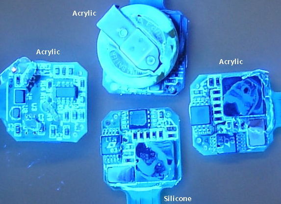
The large square chip is the logic chip on the top side, beneath the battery. Its top surface is flush with the battery bottom surface when the battery is loaded. The silicone has penetrated between the two surfaces better than the acrylic. Close inspection of the circuits reveals that both coatings cover the circuit board and resistors below the battery. Upon close inspection of all boards, we note many bubbles and imperfections in the acrylic coating, and few imperfections in the silicone. We remove the MSOP-8 package on the top side and observe both acrylic and silicone have covered 90% of the area beneath the package, as shown below.

We load a battery onto an A3028A along with three leads and antenna. We apply three coats of silicone conformal coating. We baked for at least 5 minutes at 60°C between coats and for three hours afterwards. The silicone has coated the circuit board, and had penetrated beneath the larger components, but the corners of the P0402 resistors are bare. We connect an auxiliary battery, turn the transmitter on, and find we can taste the battery voltage on the bottom side of the board. We place the circuit in water and its X and Y channels oscillate together at about 1 Hz.
No36.1, an A3028D, has been running since 31-DEC-13 and is still going strong.
[06-MAR-14] We receive this xray image of the over-molded A3028A from one of our assembly companies. The picture below is a close-up of the space under the battery, with contrast and brightness enhanced to show the cavity beneath the battery wrapper.

The space between the battery body and the top-side components is filled. The spaces between the battery tabs and the battery body are filled. If such wide, thin spaces are filled, we are hopeful that the spaces between P0402 components are also filled.
[10-MAR-14] Transmitter No36.1 is near the end of its life: battery voltage is 2.2 V. It has been running since 31-DEC-13, a total of 70 days, or 10 weeks, which is 2 weeks longer than we guarantee. We put the transmitter in water with the X and Y leads immersed and the C lead outside. We see high-frequency noise as shown below.

This noise is the same as the high-frequency noise that arises on the A3019 when there is a break inside the insulation of the X− lead.
We have 13 transmitters No38.7 through 39.5 (missing 38.6) that have been soaking in water for four days. We test reception and frequency response with 20 MΩ source. All are normal except No39.1 which has poor reception and 38.9, 38.10, and 39.2, which have gain 3 dB below normal at 100 Hz. We connect these three to a 50-Ω source and frequency response for all three is normal. We put all of them in the oven to bake.
We suggest that the low gain described in the previous paragraph is due to a capacitance between the X input and the amplified X, location shown here. The gain is normal at 10 Hz because the capacitor's impedance is much greater than our 20-MΩ source impedance. The gain drops by 3 dB at 100 Hz because the capacitor loads the source with −10j MΩ in parallel with the X input's 10-MΩ input resistor. When we drive the input with a 50-Ω source, the condensation capacitor does not load the source, so the gain is normal at all frequencies.
[12-MAR-14] Our transmitters No38.7 through 39.5 (missing 38.6) have been baked for a few hours. Gain versus frequency is nominal for all 13 transmitters. Our Octal Data Receiver is malfunctioning, giving the impression of poor reception on all channels. We replace the data receiver and all 13 transmitters have perfect reception. We measure switching noise in water.

The switching noise is no more than 6 μV and the frequency is 22±1 Hz. The variation in frequency is five times smaller than for the A3019.
Transmitter 36.1 has battery voltage 2.17 V but is still running after 72 days. It detects mains hum, heart beat from two people, and has normal noise.
[19-MAR-14] Transmitter 36.1 has battery voltage 1.94 V but is still transmitting intermittently. It records mains hum.
[21-MAR-14] We have a batch of nine A3028Es, No39.6-39.14, with 150-mm un-stretched leads. We applied acrylic coating to the critical regions of the A302801B layout. We encapsulate with epoxy, touched up with nail polish, and applied five coats of silicone. The result is a transmitters with average body volume 2.8 ml (we immersed up to the antenna base and measured total displacement of water 24.8 ml). For the past year we have been applying eight coats to rat transmitters, but we now believe eight coats is excessive, because moisture problems do not arise from penetration of the silicone, but rather through condensation inside a sealed silicone coating. We leave in water to soak.
We have a batch of four A3028Bs, No40.1-No40.4, with 50-mm un-stretched leads. We apply acrylic coating, encapsulate in epoxy, coat five times with silicone. Two of these have a gold-plated pin for the X electrode (electrode type F). We leave in water to soak.
[24-MAR-14] Transmitters No39.6-40.4 have been soaking in water for three days. Frequency response of all thirteen transmitters is within 1 dB of nominal at all frequencies. Reception is perfect in our small faraday enclosure. We obtain this plot of switching noise in No39.6-40.4 (One vertical division is 0.8 μV).
We have a yield of 13 out of 13 after a three-day soak. We resolve to ship a batch of 8 A3028Es to ION and a batch of 3 A3028Bs to Edinburgh.
[26-MAR-14] We have completed and double-checked our A302801C layout. We describe the changes and give links to new files here.
[28-MAR-14] We have an A3028A that won't turn off. It's the one we received with over-mold from an assembly company, and it has been running since at least 12-MAR-14 when we first examined it and determined that it was stuck on. So far it has seen 16 days of continuous running, and our expected battery life for this device is 15 days. Battery voltage is 2.52 V. We drop it in water with the lead ends stripped and observe noise 37 counts rms on both channels.
[31-MAR-14] The above-mentioned over molded transmitter is no longer running. Operating life for the A3028A appears to be a little over 16 days.
[11-APR-14] We assemble two A3028P single-channel transmitters for implantation in rat pups. At the moment, they have their programming extensions attached. They are equipped with freshly-charged PP031012AB 19-mA-hr lithium-ion batteries. We obtain this plot of A3028 noise when powered by a lithium-polymer battery, before encapsulation, when we expect no switching noise.
Noise amplitude in counts rms and battery voltage in Volts are as follows; No40.6: 19.4 and 4.3 V, No40.7: 17.5 and 4.3. For comparison we have an A3028A with a fresh, BR2330 battery with No13 34.0 and 3.0, No14 33.0 and 3.0. With battery voltage 4.3 V, one count is 650 nV, and for 3.0 V one count is 460 nV. We expect the noise amplitude to drop from 33 to 23 counts rms when we increase battery voltage from 3.0 to 4.3 V.
The center of the RF spectrum of both A3028Ps lies within 913-918 MHz. The transmit clock period lies within 195-215 ns. Reception in our faraday enclosure is perfect. Dynamic range at the X input is 43 mV. Gain and frequency response is nominal for both devices.
We find burrs on the battery wire solder joints. We re-solder the joints and wash the device with the battery still attached. Both batteries lose voltage. One appears to be discharged and accepts a re-charge. The other will not re-charge. We replace the batteries and epoxy them as before.
[14-APR-14] Transmitters No40.6 and 40.7 look good, but No40.6's battery is drained for reasons we cannot explain. We did not leave the enabling jumper in place, so the battery should have been isolated. We recharge both batteries and monitor their battery voltages through their X measurement with the Receiver Instrument and a 200-Ω resistor draining the battery directly.

The 200-Ω resistor load drains the battery almost the maximum recommended rate. By the time we end the experiment, No6's battery has delivered 12 mA-hr and is down to 2.5 V. The transmitter stops working. No7's battery has delivered 14 mA-hr and its battery voltage is still 3.5 V. The No6 battery has been damaged by over-discharge, but still provides more than half its nominal capacity.
We encapsulate two A3028Ps. One was faulty before, both were faulty after. The first one, No6, draws 800 uA when asleep and 900 uA when awake. Even when asleep, it will drain its battery in about twenty-four hours. This explains why it worked when we first assembled it, then the battery was completely drained after a day. When it is awake, it transmits fine.
The second one, No7, draws 2.0 uA, but when you turn it on it draws 170 mA, which is enough to generate heat, and it does not transmit. So we let it sit like that for a while and then feel the various parts It turns out to be the RF oscillator, U9, that's faulty. Further inspection reveals that the unused pad under pin U9-1 has shifted over and is touching U9-2. By this time we knocked off the BGA-5 chip, and can't get another on there because of all the silicone.
We conclude that both circuits were damaged during experiments and encapsulation. We should try again.
[05-MAY-14] We have a batch of ten A3028Es, No40.12-41.7, and two A3028Bs, No40.9-40.10. They have been soaking in water for five days, with three lots of hot water to provoke internal condensation. We measure gain versus frequency and find it to be within 1 dB of nominal for all transmitters. Switching noise peaks are all in the range 20-24 Hz, peak amplitude 5 μV, average amplitude 2 μV. No sign of spikes on No40.12, which has amplitude 5 μV. Thus we have all twelve transmitters functioning perfectly.
[09-MAY-14] We have two A3028P rat pup transmitters. We put them in hot water yesterday and left them soaking while turned off. Here they are after blow-drying, along with a non-functional model we assembled earlier. The model shows how we want the antenna and leads of the A3028P to be arranged, in a plane. The two working prototypes have their leads and antenna coming coming off the circuit board at odd angles.

We hope to fix the direction of the leads in future assemblies. In water, we measured battery voltage and noise amplitude before soaking yesterday and obtained for No41.8 4.2 V and 9 μV and for No41.9 4.1 V and 8 μV. Today we obtain for No41.8 4.1 V and 7 μV and for No41.9 4.2 V and 10 μV. We measure frequency response and find it to be within 1 dB of nominal for both.
[12-MAY-14] No41.8 and 41.9 still transmit a strong signal. Analog gain is 30 dB too low. We backe both in the oven for half an hour and 41.8 recovers fully, showing correct gain with frequency, while 41.9 shows some improvement. Leave them in the oven.
[14-MAY-14] No41.8 and 41.9 now working well. Battery voltage is 4.1 V. Frequency response is within 1 dB of nominal.
[19-MAY-14] New batch of transmitters, No41.10-42.9 placed in hot water and allowed to cool and soak for four days. Today we measure frequency response. All are within 1 dB of nominal except for No42.2, which is 2 dB below nominal at 130 Hz, there being no bump in the response before the cut-off. We measure switching noise, and obtain this plot showing noise less than 5 μV and within the range 21-23 Hz.
[28-MAY-14] We receive a batch of 50 of our A3028 assemblies with A302801B circuit board from Advanced Assembly. Below is one of the x-ray images of the two BGA packages we received from them.

We program and calibrate ten circuits, and test the magnetic switch, which remains a BGA-5 in this version of the circuit board. All work fine. There is no sign of the problems we have had in the past with the BGA-5.
[09-JUN-14] We have two new A3028P pup transmitters No43.10 and 43.11. They have been soaking for four days in water. We used acrylic coating on the analog circuits prior to applying three coats of silicone by dipping. Batteries are sealed with epoxy then three coats of silicone by dipping. The antenna is 45 mm long and bent into a tighter loop.

In our faraday enclosure we obtain 100% reception from both transmitters when they sit on our antenna. We place No43.10 and an A3019D No29.12 on an A3015C Loop Antenna on our table. We place the transmit antenna loops right on the A3015C surface, so the batteries are on top. Reception is 100.0% for both. We place the battery side down. Now the A3028B batteris is between the receive and transmit antennas. Reception is 59.9% from the A3028P and 99.9% from the A3019D. The A3028P should be implanted with the battery facing the body and the antenna facing the skin.
We measure frequency response. Gain is within 1 dB of nominal from 0-250 Hz for both transmitters. We place in water to measure noise and battery voltage. For a few minutes, No43.10 shows transients up to full scale, with frequency a few Hertz. It settles down to an average of 28500 counts and 14 counts rms, so battery voltage is 4.1 V and noise is 9 μV. No43.11 shows no transients, battery voltage 4.1 and noise 10 μv.
We have fourteen A3028E transmitters 42.10-43.9. They have been soaking in water for ten days, including three hot-water soaks. No42.10 won't turn on. Frequency response of all remaining transmitters is within 1 dB of nominal. Switching noise is less than 3 μV for all. Transmitter No43.4 has a flaw in its blue lead. We have twelve that are ready to ship.
[13-JUN-14] We have 5 of A3028AV2 made with A302801C circuit boards. See here for photograph of top side. The two large holes are for the BR1225 battery. When we load the battery into these holes, it is centered perfectly on the square of the circuit board. Note barrier pads in top-right near X and Y inputs. We program four as dual-channel and one as single-channel transmitters. We use the new V4 firmware, which provides compiler directives to select A302801B and A302801C circuit boards. We measure gain versus frequency and find it to be within ±1 dB for all channels and frequencies.
[19-JUN-14] We receive an A3028AV2 on an A302801C circuit board with leads, antenna, and battery loaded, and new over-mold applied. See photograph below.

The A3028AV2 over-mold is 7.7 mm high and 13.6 mm square. With two coats of silicone, the device will be 8.2 mm high and 14.1 mm high. Two coats may not provide a reliable seal over the irregularities in the mold surface. With three coats of silicone, we should get a good seal, but the device will be 8.4 mm high and 14.4 mm square. Our hand-encapsulated A3028A is not rectangular. Its height is varies from 8.0 to 8.4 mm and its width from 13.4 to 15.3 mm.
We program and calibrate the over-molded circuit. It works well with an external battery. It does not work with its internal battery. The internal battery voltage drops from 2.5 V to 1.0 V when we close the internal battery switch. The battery is exhausted. We connect another battery in parallel. After a few minutes, the internal battery voltage has risen to that of the external battery. Roughly 0.3 μA flows into the circuit. We close the internal battery switch. The external battery supplies 56 μA through R1 (2.7 V / 50 kΩ). We turn on the transmitter. The external battery supplies 187 μA (56 μ + operating current of dual-channel transmitter). We conclude that the internal battery is exhausted.
[20-JUN-14] At one of our assembly companies, they find that the batteries we sent them a month ago are all drained of charge. We sent the batteries in anti-static foam, which is electrically conducting.
We note that the circuit board entering the over-mold is at a slight angle to the horizontal, as a result of tension in the antenna and leads. The antenna and leads emerge vertically and must be bent to go horizontal. Instead of soldering the leads through the holes, we now plan to solder them as shown below.

The pads two which the leads are soldered are all secured by through-plated holes. The leads are secured by a rivet of solder.
[25-JUN-14] Transmitters 43.12-44.7 have been soaking in hot and cold water for a week. We measure frequency response, reception, and noise. All give gain within 1 dB of nominal for 0-250 Hz, reception 100% in faraday enclosure, and noise less than 40 counts rms after dropping in water. The plot below shows the switching noise in a 32-s interval.

Peak switching noise is 6.4 μV. We see the second, third, and fourth harmonics of the switching noise clearly in the spectrum.
[02-JUL-14] We have A3028AV2 encapsulated in epoxy and silicone with no acrylic coating on the EEG amplifiers. We want to find out if the barrier pads of the A302801C layout, and its greater separation between the input and output components, will eliminate condensation faults without the acrylic coating. These five transmitters have been soaking in water for a week with four hot water charges. They are No45.1 (A3028D), No45.3 (A3028D), No45.5 (A3028A), No45.7 (A3028D), and No45.8 (A3028B). Thus all but the last one are dual-channel. We connect to our 20-MΩ sinusoidal source and find the gain of the dual-channel devices lies within 1 dB of nominal. The difference between channels is less than 0.2 dB. Device No45.8 has gain 1 dB higher than normal from 1-20 Hz, nominal gain 20-110 Hz, shows only a 1-dB increase in gain at 130 Hz instead of 3 dB, and has the correct cut-off frequency. We place No45.8 in parallel with one input of No45.5 and note that the two have the same response to within 0.2 dB up to 110 Hz, when No45.8 is 2 dB too low. None of the transmitters generate a square wave when left open-circuit.
[03-JUL-14] After twenty-four hour bake at 60°C, No45.8 has nominal gain from 1-110 Hz, shows only a 1-dB increase in gain at 130 Hz, and has the correct cut-off frequency. Yesterday, before baking, the gain was 1 dB higher than nominal from 1-20 Hz, which is within specification. The lack of a 3-dB bump in gain at 130 Hz is out of specification, but persists after baking. So far, these first five A3028AV2s, encapsulated without acrylic coating, show not sign of condensation problems. Peak switching noise for the five transmitters is 4 μV in the range 20-22 Hz with both channels of each dual transmitter agreeing about the amplitude of the switching noise.
We have A3028AV1 circuits encapsulated with acrylic, epoxy, and silicone, No44.8-44.14, No46.1-3, all A3028B single-channel mouse transmitters. These we made with wires soldered flat on the pads, as shown here. The result is leads that emerge in the correct direction without bending. Frequency response of all amplifiers within 1 dB of nominal. Switching noise 6 μV maximum. We measure volume by displacement of water and get 1.36 ml each. We measure by weighing in and out of water and get 1.45 ml. On average, around 1.4 ml. Mass is 2.7 g.
[31-JUL-14] We have 12 of A3028E-AB, No46.5-47.2 that have soaked in water for five days. We measure gain versus frequency, all are within ±1 dB of nominal. We measure reception, all are 100% in enclosure. We measure switching noise and all 20-22 Hz, 0-6 μV. All turn and off multiple times without error.
We have No45.11 A3028A with thermoplastic over-mold and one coat of silicone. The one coat leaves visible cavities around the electrode leads. We left it soaking in water for three days. Now its battery voltage is 2.0 V, reception is poor, and gain is 20 dB too low.
We have No48.1 A3028A with thermoplastic over-mold and three coats of silicone. There are no visible cavities in the coating. We left to soak for three days. Its battery voltage is now 2.7 V, gain versus frequency within 1 dB of nominal, and within 0.2 dB between channels. Switching noise is 1.2 μV at 19.5 Hz. Reception is good. Magnetic switch is working well.

The transmitter body fits in a rectangular volume 14.3 mm × 14.0 mm × 8.5 mm = 1.7 ml. The volume occupied by the transmitter is 1.6±0.1 ml. Our most compact hand-encapsulated A3028A has volume 1.4±0.1 ml. The three coats we applied to No48.1 increased its thickness from 7.8 mm to 8.5 mm. This accumulation agrees well with the 125 μm per-coat thickness specified in the MED10-6607 data sheet.
[13-AUG-14] We have 9 of A3028B, No40.8, 40.11, 47.3, 47.6, 47.7, 47.9, 47.10, 47.12 and 2 of A3028A, No47.4 and 47.13. They have been soaking for four days. All are within ±1 dB of nominal frequency response. All give 100.0% reception in enclosure. Switching noise is 8 μV for No47.4 (both channels the same). Others have less switching noise. Magnetic switches all respond well.
[03-SEP-14] We have 8 of A3028B-CC, No49.2, No49.5-No49.11. We note that 49.11 is labelled 49.3 so we apply colored silicone over the label to obscure it. All transmitters produce less than 8 μV of switching noise and have frequency response within 1 dB of nominal. Reception is 100.0% in a faraday enclosure.
[12-SEP-14] Transmitters A3028E-FB No42.8, 44.6, and 44.5 have failed at Philipps University, Marburg after eight weeks implanted. No42.8 works fine, except it keeps turning itself off. This circuit was one upon which we replaced U3 by hand. No44.6 and No55.4 have exhausted their batteries. Even if they were left on from the moment we shipped them, they should still be running. We suspect excessive current consumption, which is a problem we observed in some members of the batch of circuits from which these two were taken.
We have a new batch of 100 circuits in which U3 is a UDFN-6. They work fine, except two out of twenty so far have had a short between U3-1 and U3-6. The assembly house glued U3 in place, so we must remove it with pliers. We replace and the board works fine. We note that the spacing between U3-1 and U3-6 is too small. The U3-1 pad is too large. We create A302801D layout and reduce the pad from 19 mils to 16 mils.
[22-SEP-14] We have a batch of twelve transmitters No49.14-50.11. All have been soaking in water for three days. All have frequency response within 1 dB of nominal, perfect reception in a faraday enclosure, and switch noise less than 6 μV.
[23-SEP-14] We hear from Pishan at UCL that 44.10 had symptom "no signal" after implantation on 11-AUG-14. This transmitter was shipped on 03-JUL-14, so it is possible that, once it arrived at UCL, it turned on and has since exhausted its battery.
[01-OCT-14] We have transmitters A3028E-AB No50.14-51.13. The silicone has cured for two days, but we have not soaked in water at all. We must ship them today. All have gain within 1 dB of nominal, perfect reception. We ship all but No51.3 and No51.4, which stuck together during curing, so we must touch up the outer coat. Switch noise is less than 6 μV for all the transmitters we shipped.
[03-OCT-14] Transmitter 50.12 and 50.13 are encapsulated in acrylic conformal coating and silicone. We injected silicone under the battery twice and dipped four times. Battery voltage is 2.5 V for some reason, but frequency response is within 1 dB of nominal. We place in water. Two hours later, No50.13 still had nominal frequency response, but No50.12 is generating a 1-Hz full-scale square wave.
[06-OCT-14] Transmitter 50.13 has been sitting in water. Its gain is 20 dB too low when driven by a 20-MΩ source impedance. We connect it in parallel with another transmitter and the gain of both is now 20 dB too low. We drive 50.13 with a 50-Ω source and we obtain nominal gain at 10 Hz, 3 dB too low at 100 Hz, and 6 dB too low at 130 Hz. We place 50.12 and 50.13 in the oven at 60°C
[08-OCT-14] After 48 hours in the oven, 50.12 and 50.13 both perform perfectly.
[10-OCT-14] Put batch No51.14-52.13 in water. Kirsten tells us she is certain she forgot to put the acrylic coating on the circuit boards.
[14-OCT-14] Batch No51.14-52.13 still soaking in water, turned off. These are A3028V2 made with the A302801C circuit board. We check frequency response on all 14 transmitters and find it to be within 1 dB of nominal in all cases. We leave in hot water.
[15-OCT-14] We examine 50.12 and 50.13 closely. Both have many bubbles in the acrylic coating around the amplifier parts. We consider whether there is a reaction between the acrylic coating and directly-applied silicone dispersion. We apply two coats of acrylic to a bare circuit board, then coat with silicone and see no bubbles. We have observed such bubbles when acrylic coating is tacky due to drying out. Transmitters 50.12 and 50.13 were made with tacky acrylic. Each transmitter has a deep hole behind the battery terminal, leading to the interior space beneath the battery. We fill these holes with a syringe and leave to cure. We review our history of acrylic coating and condensation-related problems. We started applying acrylic in September 2013 with the A3019A/D transmitters. We saw an immediate reduction in the incidence of condensation problems after our four-day water soak. As we moved to water washing and complete acrylic coating, condensation problems disappeared. Thus we believe the acrylic coating solved the A3019 condensation problem. The A3028V2 introduces a new layout with barrier electrodes and more distance between EEG amplifier input and output. Both 50.12 and 50.13 are A3028V2s. We have had no condensation problems with this circuit until the 50.12 and 50.13. Our hypothesis now is that an imperfect acrylic coating (bubbles) combined with an imperfect silicone coating (holes) resulted in condensation problems even with the new A3028V2 layout.
[19-OCT-14] At ION, transmitter No13, we're not sure which batch, has failed after several days implanted with an ISL. Its last moments are shown here.
[20-OCT-14] Two more transmitters have failed at Philipps University, Marburg. The screen shot below shows the recording shortly before failure from transmitters No50.1 and No50.2.

The average value of signal No50.2 in this interval, and more clearly in later intervals around 170 s, is around 20,000 counts, which implies a battery voltage of 6.0 V. The maximum possible voltage supplied by our lithium primary cell BR2330 is 3.0 V. When the average converted value is 30% of the full scale, the X input to the ADC (pin U7-2, see schematic) must be only 30% of the ADC power supply (VA). But the average value of this X input is 1.8 V when the amplifier is working correctly. Thus the amplifier is damaged.
The high frequency noise on No50.2 at 37-38 s has power from 75 Hz all the way up to 255 Hz. At time 192 s, there is full-scale noise from 0-255 Hz. The gain of the amplifier at 255 Hz is only 1, so a full-scale 255 Hz implies a 2.7-V 255-Hz signal at the X input electrode. Assuming such an input is impossible, the amplifier must be generating this signal itself, which implies it is damaged.
The Philipps University experiment involves stimulating the brain with 20-V pulses, 40 ms apart, 0.1 ms duration, at 2 Hz, as well as more sustained stimuli every minute or two. The trace below shows two sets of pulses.

The pulses are around 2 mV peak to peak. The more sustained stimuli reach an amplitude of 4 mV. Looking at these traces, we see no reason to suppose that the input to our transmitter is being driven by a signal outside the absolute maximum ratings of op-amp U5. The inputs are clamped by diodes inside the op-amp to its power supply voltages. Nevertheless, if we were to apply 20 V through 10 kΩ to the X input, we would see around 17 mA flowing through these clamping diodes, which exceeds their maximum rating of 10 mA. Thus it is possible to damage the transmitter with a 20-V stimulus delivered through brain tissue. Damaged op-amps can develop erratic input offset voltages and consume excessive current. If U5 starts to consume 1 mA, VA will drop to 1.7 V and the ADC will stop working. It will produce only 0's or 1's. We see such intervals in the No50.2 recording. Furthermore, the battery will drain in about ten days.
[20-OCT-14] After two more injections of silicone, making six in all to fill the holes behind the battery terminals, we are satisfied that No50.12 and 50.13 are sealed, so we put them in water.
[20-OCT-14] Batch No51.14-52.13 has soaking since 10-OCT-14. This is the batch with no acrylic coating. Gain versus frequency is within 1 dB of nominal for all transmitters.
[21-OCT-14] We have No44.10 back from UCL. We shipped this device on 03-JUL-14 and Pishan implanted on 11-AUG-14, at which point she discovered that it would not turn on. We find the exterior silicone in perfect condition, the epoxy in perfect condition, and the leads also. we cut away enamel and epoxy to get to the battery terminals. The battery voltage is 0.13 V. We apply 3.6 V and 600 μA flows into the dead battery. We can turn on and off the transmitter easily. The analog input shows mains hum. We drop the applied voltage to 2.7 V. After a few minutes, off-state quiescent current drops to 7 μA. We turn on and current increases to 85 μA. This transmitter, when calibrated, had on-state current 79 μA and off-state current 2 μA. If we assume that we still have 2 μA flowing into the circuit in the off-state, then 5 μA is flowing into the battery, which means the on-state current is now 80 μA, which is very close to the original 79 μA. Our best guess as to why this transmitter failed is that it was left on and drained its battery.
[21-OCT-14] Silicone-encapsulated No50.12 and No50.13 have been in water for 24 hours. No50.13 shows −6 dB gain versus frequency, but normal bump and cut-off frequencies. No50.12 won't turn on. We strip silicone from the underside and measure battery voltage 2.6 V. Now it turns on. Gain is correct at 1 Hz and drops off rapidly above that, with random drifting baseline in the signal.
[21-OCT-14] We receive this diagram of the electrode arrangement at Philipps University, Marburg.
[20-OCT-14] Batch No51.14-52.13 has been in water since 10-OCT-14. Gain versus frequency remains within 1 dB of nominal. We switch cold for hot water. We measure switching noise and perform harmony test. All transmitters appear to be perfect. We leave them switched on and in water.
[22-OCT-14] Batch No51.14-52.13 all running, noise is normal. Average voltages are between 69% and 71% of full scale.
[22-OCT-14] Batch No52.14-53.13 has been sitting in water for 5 days. Noise is normal. Reception is perfect. Gain versus frequency within 1 dB of nominal except for 53.7, which is 1 dB below nominal at 140 Hz. Magnetic switches all reliable.
[24-OCT-14] Batch No51.14-52.13 has been running in water since 20-OCT-14 and soaking since 10-OCT-14. Noise is normal. Average voltage is 70% of full scale. Frequency response within 1 dB of nominal.
[27-OCT-14] Batch No51.14-52.13 has been running in water since 20-OCT-14 and soaking since 10-OCT-14. Average voltage is 70% of full scale except for 52.1, which is at 84% of full scale, with occasional steps lower or higher. The battery voltage appears to be around 2.1 V. When we apply a 10-mVpp input, we see saturation and inversion of the positive cycles at the top end of the amplifier's dynamic range. We reduce the amplitude to 3 mVpp and observe frequency response within 1 dB of nominal. Reception is 100.0% within our faraday enclosure. All others show perfect reception, normal switch noise, and frequency response within 1 dB of nominal.
No52.1 We remove silicone and release the +ve battery tab. We measure 2.27 V between the circuit VB pad and the positive battery tab. When we connect with an ammeter, we observe 1.6 μA in the inactive state and 7 mA when we switch on. At 7 mA, the battery would last only 36 hours, but 52.1 ran for four days with no change in battery voltage. We burn off epoxy over the -ve battery hole and connect 2.7 V. Inactive current is 1.9 μA, active current fluctuates between 12-15 mA. We connect 2.7 V directly to VD (using R4). Current is 13 mA. We activate and deactivate the magnetic switch. Current remains unchanged. After a few minutes, current is 9 mA. We increase the supply to 3.9 V and current increases to 20 mA, then drops over a few minutes to 15 mA. We remove U1 to make sure we have no current going back to the magnetic switch. Current is 16 mA at 3.1 V. We remove R4 and current is 14 mA at 3.1 V. Signal output is stuck at 0, but reception is perfect. We observe bursts of 910-MHz power every 2 ms in the RFPM Instrument. We compare spectrometer plot with an encapsulated transmitter and find peak power to be within a few dB. We remove U9. We now have no RF output, but current is 18 mA at 2.7 V. Remove U4. Current remains 18 mA at 2.7 V. We remove C3. Current drops to 20 μA, the correct quiescent current of U7 if supplied with 1.8 V. We are holding C3, preparing to measure its resistance and capacitance, when it shoots out of the tweezer tip and vanishes.
[28-OCT-14] Transmitter 50.5 has failed by discharging its battery while implanted at Philipps University. Looking at their recordings, it appears that a No7 transmitter is about to fail also.
According to the engineers at AVX, excessive leakage current in capacitors is caused by internal cracks, but its manifestation can be delayed by several months. The capacitor can be cracked during pick and placement at the assembly house, during depanelization, and during subsequent soldering near the capacitor. According to Ikeo et al. (Failure Mechanisms that Cause High Electrical Leakage in Multilayer Ceramic Capacitors), ceramic capacitors can fail by degeneration of their insulation layers resulting their behaving like resistors of a few hundred Ohms. The cause of degeneration they investigated is a voltage-driven chemical reaction assisted by the penetration of water and chloride ions into the capacitor through cracks or microscopic pores.
When we solder the antenna onto the A3028 circuit board, we use zinc chloride flux (acid flux) and high temperature. Capacitor C3 is the power supply decoupling capacitor for the radio-frequency oscillator. We give the location of this capacitor for various transmitters in the following table.
| Version | Capacitor | Distance to Pad (mm) |
Distance to Board Edge (mm) |
|---|---|---|---|
| A3019 | C7, 1nF | 0.36 top side | 0.33 |
| A3028V1 | C3, 1nF | 1.6 bottom side | 2.4 |
| A3028V2 | C3, 1nF | 1.0 bottom side | 0.41 |
| A3028R1 | C3, 1nF | 0.58 bottom side | 2.1 |
We shipped hundreds of A3019s and never observed this sudden discharge problem, even though we soldered with acid flux directly on the circuit board next to the capacitor, and we broke the circuit boards apart from one another by hand. This suggests that the problems with the capacitors on our new circuit boards is not with our soldering procedure, but either at the manufacturer or at the assembly house. We shipped a hundred A3028V1s and may have observed one such failure at ION recently (No13 see 19-OCT-14). The A3028V2 assembly we have been shipping since late September has shown 1 such failure out of 14 in our office, and at least 3 such failures out of 14 at Philipps University. Transmitter 50.7 may be failing the same way as we write. Transmitter 50.2 showed full-range oscillations at hundreds of Hertz, which could be caused by a leaky capacitor for C11.
We recently started cleaning the boards with a finer brush, which may be getting under the capacitors and cracking them. We will stop using this brush. We will examine all 1-nF capacitors on our A3028V2 boards for cracks. We will pre-tin the steel leads, wash them, and solder them with normal flux to the circuit boards. This will reduce the amount of chloride near the decoupling capacitor. But we suspect that we will see no cracks, because the cracks are internal, and that the damage was done during assembly, before the boards ever arrived at our office. Thus we will replace C3 on all boards.
[29-OCT-14] Transmitter 50.7 failed today at Marburg. Of the batch of 12 we sent them, 4 have failed by sudden battery drain and 1 by something crazy in the EEG amplifier.
We inspect the 1-nF capacitors on the bottom side of half a dozen A3028V2 circuit boards. These are C3, C9, C10, and C11. The figure below shows C9 and C10 on the circuit board with assembly company serial number ending in 049.


Looking closely at the top side of C9, we see a chip on the edge and a semi-circular mark. This mark is, we believe, the outline of the vacuum pick-up bit used to place the capacitor during machine assembly (see Figure 7 here). When too much force is exerted by the bit, such marks appear on top, and cracks occur on the bottom. Any crack in a capacitor is a means by which moisture can penetrate and, when voltage is applied, cause degeneration of the insulation.
Meanwhile, batch No51.14-52.13 has ben running in water since 20-OCT-14 and soaking since 10-OCT-14. No52.1 drained its battery two days ago. No further failures have occurred.
[30-OCT-14] Batch No51.14-52.13 has been running in water since 20-OCT-14 and soaking since 10-OCT-14. Thirteen of them remain working. Battery voltage is 2.66 V on average with standard deviation 16 mV. Frequency response is within 1 dB of nominal for all devices except 52.6, which has gain 1.5 dB above nominal at 140 Hz. We place transmitters 45.1, 45.3, 49.12, 49.13, 51.3, 51.4, 52.14, 53.13 in water, all turned on. We checked some of their frequency responses, and all of their battery voltages. We turn on acrylic and silicone encapsulated 50.3. Its gain versus frequency is once again with in 1 dB of nominal. We leave it running in water also.
We place a transmitter on a horizontal antenna in a faraday enclosure. We measure the power picked up by the antenna in four different orientations of the antenna. We do this with two mouse transmitters and receive up to −44 dBm from one and −40 dBm from the other. We repeat with three rat transmitters and receive a maximum of −42 dBm and −40 dBm from each. We perform the same experiment, but the transmitter is in a jar of water resting on the antenna. We receive up to −42 dBm from a mouse transmitter and up to −40 dBm with a rat transmitter. We placed the transmitters in a small petri dish of water. We obtained up to −36 dBm from a rat transmitter and −38 dBm from a mouse transmitter.
[03-NOV-14] Transmitters No51.14, 52.2-52.13 have been running in water since 20-OCT-14 and soaking since 10-OCT-14. Transmitter No52.6 generates its own sinusoid of amplitude 13,000 counts at 100 Hz when its input is driven by 0V through 20 MΩ. With inputs open-circuit, frequency drops to 80 Hz and amplitude increases to 22,000. When driven by a 10-mVpp, 50-Ω sinusoid, gain is 6 dB too high, but the shape of the gain versus frequency is within 1 dB of nominal. When connected in parallel with another 51.14 to 60 mVp-p through 20 MΩ, the gain versus frequency of the two transmitters is identical and correct. On its own again, with 20 mVp-p through 20 MΩ and we no longer see a square wave, but gain is 10 dB too high at 100 Hz. Place in parallel with No52.7 and gain versus frequency for the two is identical but 10 dB too high at 120 Hz. We put No51.14 in parallel again with 60 mVp-p through 20 MΩ and get identical gain, but gain is 7 dB too high at 120 Hz. Reception for No52.6 is perfect and noise is normal when in water. This transmitter has the square wave problem, and it appears to be varying in its severity as we perform our experiments. Transmitters No51.14, 52.2-52.5, 52.7-52.13 all have gain within 1 dB of nominal, perfect reception, and normal noise. In water, average signal is between 66% and 69% of full scale, indicating battery voltages 2.60-2.73 V.
Transmitters 45.1, 45.3, 49.12, 49.13, 51.3, 51.4, 52.14, 53.13 have been running in water since 30-OCT-14. Transmitters 45.1 and 45.3 are both dual channel. The figure below shows the frequency response of both channels in parallel for 45.1.

For similar plots for other transmitters see No45.3 (dual channel also), and No49.12, No49.13, No51.3, No51.4, No52.14, No53.13. All are within 1 dB of nominal, with No49.12 having gain 1dB above nominal at 120 Hz. Transmitter No50.13, which is acrylic and silicone coating, has gain 14 dB below nominal at 1 Hz, and 20 dB below nominal at 120 Hz.
Batch 54.1-54.10 has been running in water for three days. Average signal values 67-68% of full scale. The same is true for dual-channel 54.13 and 55.1. We measure gain versus frequency for the dual channel transmitters and find it to be within 1 dB of nominal.
[06-NOV-14] After baking, transmitter No52.6 shows gain versus frequency within 1 dB of nominal except at 120 Hz, where it is 1.5 dB above nominal. We set this one aside as a demonstration transmitter.
[07-NOV-14] After a total of five days running in water, we ship transmitters 52.14, 53.13, 54.3, and 54.4 to ION for job 1161.
[10-NOV-14] We have transmitters 49.12-13, 51.3-4, 54.1-2, 54.5-10, 55.1 (two-channel) running in water for a total of 4 + 5 = 9 days. Average signal values are all 67-69% full scale, except for 51.3, which is at 73%, indicating a battery voltage of 2.45 V.
No51.3 We check gain versus frequency for 51.3 and find it within 1 dB of nominal. Battery voltage remains 2.45 V. Silicone encapsulation looks intact all around. No sign of condensation inside. We remove silicone and disconnect positive battery terminal. We measure inactive current 1 μA and active current of 550 μA. We remove C3. On current is now 600 μA. We remove C5 and on current drops to 80 μ. We measure the capacitance of C5, it is 9 μF. Insulation resistance is greater than 20 MΩ. According to here, "Failed capacitors frequently recovered their insulation resistance at high temperature (above +200°C)." When we removed C5 with a soldering iron, we heated it to 400°C.
We hear from ION that 53.3 and 53.6 have failed after three days implanted, following a 5-day active soak. We do not yet know the nature of the failure. We place 49.12-13, 51.4, 54.1-2, 54.5-10, 55.1 in a jar of water in the oven at 60°C. All are running.
We receive from Philipps transmitters 43.3, 43.7, 50.1, 50.2, 50.5, and 50.9, all A3028Es. No43.3 Antenna is cut, red lead cut short. Reception 100%, picking up mains hum, average value with mains hum is 40,000. Gain versus frequency within 1 dB of nominal. Severe discoloration of purple enamel. No43.7 Reception 100%, picking up mains hum, average value 43,000. Gain versus frequency within 1 dB of nominal. Severe discoloration of purple enamel. No50.1 Reception 0%. Large cut across silicone on battery side. Open up encapsulation. Battery voltage is 2.1 V. Apply external 2.6 V. Inactive current 2 μA, on current 80 μA. Reception 100%, picks up mains hum. No50.2 Reception 0%. Open up encapsulation. Battery voltage 2.4 V and falling. Active current 2 μA, inactive current 80 μA. Picks up mains hum. Average signal 41.700 with 2.8 V applied. No50.5 Reception 100%, picking up mains hum, average value 51,000, gain versus frequency within 1 dB of nominal accounting for low battery voltage. Open up encapsulation. Battery voltage 2.4 V steady. Inactive current 2 μA, on current 80 μA. No50.9 Reception 0%. Open up encapsulation. Battery voltage 2.4 V and falling. Inactive current 2 μA, on current 7 mA. Reception when on is 100% and picks up mains hum. Heat up and then remove C3, C5, and C4. When we remove C4, on current drops to 80 μA.
[11-NOV-14] The average battery voltage today for 49.12-13, 51.4, 54.1-2, 54.5-10, 55.1, after 14 hr at 60°C running in water, is 2.83 V with standard deviation 0.025 V. Later in the day, after 24 hr at 60°C, No49.13 average value is at 90% of full scale, and No54.2 is at 73% of full scale. The others are still normal.
[12-NOV-14] Transmitters 49.13 and 54.2 are both draining their batteries. No49.13 Reception 100%. Open up encapsulation. Battery voltage 2.2 V. Inactive current 2 μA, on current 80 μA. No54.2 Reception 100%. Open up encapsulation. Battery voltage 2.4 V. Inactive current 550 μA, on current 600 μA. Remove C6, C5, C2. After removing C2, inactive current is 2 μA and on current is 80 μA. Later in the day, 54.6 is at 64% while the others remain at 68%.
[13-NOV-14] No54.6 does not transmit. Transmitters 49.12, 51.4, 54.1-2, 54.5, 54.7-10, and 55.1 all have average signal 67-69% of full scale. They have been running in water at 60° for a little over three days. We turn them off, dry them, and put them in the oven to recover. The black enamel of No54.6 has a pale discoloration. We open up the encapsulation. Battery voltage is 2.4 V. Inactive current 2 μA, on current is 1.5 mA. We heat up C5 with a lump of solder, but do not remove it. On current drops to 80 μA.
[21-NOV-14] We have batch E55.5, E55.6, B55.10, B55.11, A55.13, E56.1, E56.2, and D56.3 (the letter gives the version). We encapsulate without acrylic coating. We use DP270, a black potting epoxy with 60-minute work life. We coat four times with silicone. We turn them off and place in water on the morning of 19-NOV-14. Today we measure frequency response. All are within 1 dB of nominal, except for channels D56.3X, E55.6, E56.1, A55.13X, which have peak gain 1 dB higher than nominal. We put them back in water.
[25-NOV-14] We have batch R60.1-14 encapsulated with acrylic, EP965L epoxy, and four coats of silicone. We measure gain versus frequency and find it within 1 dB of nominal except for R60.1 and R60.2, which have gain 1 dB too low at 140 Hz. Reception is 100% for all transmitters. We calibrate our spectrometer with 910 MHz and measure center frequencies for R60.1-14 and obtain 920, 920, 920, 917, 923, 917, 919, 916, 917, 919, 916, 918, 918, 920 MHz respectively. Transmitter R60.5 is the one at 923 MHz. Switching noise is less than 4 μV for all devices. We place in water in the oven at 60°C at 9:00 am.
[26-NOV-14] Batch R60.1-14 have been running in water at 60°C for 36 hours. We replace 60°C water with 20°C water. Average signal values are 64-66% of full scale. Gain versus frequency within 1 dB of nominal. Reception excellent from all 14 simultaneously on one antenna. Switching noise normal. We apply three more coats of silicone to R60.5. The result is unattractive. We return all of them to the oven.
Batch E55.5, E55.6, B55.10, B55.11, A55.13, E56.1, E56.2, and D56.3 has been soaking in water at 20°C for one week. We measure frequency response. All are within 1 dB of nominal. We note that this batch has no acrylic coating. We turn them off and put them in hot water.
[28-NOV-14] Batch R60.1-14 have been running in water at 60°C for 72 hours. We cool them down. Battery voltages are normal, gain versus frequency is within 1 dB of nominal for all fourteen transmitters, noise is normal. We turn them off and put them back in the oven in a tray to dry out.
[03-DEC-14] Batch E55.5, E55.6, B55.10, B55.11, A55.13, E56.1, E56.2, and D56.3 has been soaking in water at 20°C for two weeks. Frequency response is within ± 1 dB of nominal, except D56.3X, E55.6, and A55.13X, which have peak gain 1 dB higher than nominal. Average values 44-45k, except A55.13 which is at 47k. We turn them off and put them in hot water.
[05-DEC-14] Rob Wykes at ION turned on Batch 52 and put them in water at 60°C for three days. At the end, he made the following observations.

We advise Rob that all four of the transmitters that were inactive upon removal are most likely faulty. This brings to 23 the total number of A3028E-ABs we must replace for ION.
[05-DEC-14] We have Batch R61.1-14 of A3028R-AB devices encapsulated with acrylic, epoxy, and silicone. We turn them all on and poach them for two hours at 60°C. Average signal value is 64-66% of full scale. We return them to the oven, running in water at 60°C.
[08-DEC-14] Batch R61.1-14 has been running in water at 60°C for three days. We put them in cold water. Average signal value is 64-66% of full scale, except 61.14 which is 69% of full scale. Switching noise less than 6 μV. Gain versus frequency within 1 dB of nominal for all devices.[11-DEC-14] Batch E55.5, E55.6, B55.10, B55.11, A55.13, E56.1, E56.2, and D56.3 has been soaking in water at 20°C for three weeks. Frequency response is within ± 1 dB of nominal, except D56.3X, E55.6, and A55.13X, which have peak gain 1 dB higher than nominal.
[15-DEC-14] Batch R62.1-14 has been running in water at 60°C for four days. We checked that they were all transmitting and that switch noise was normal after a few hours in water, but did not measure frequency response before the poach. Today we find that all transmitters are still running. We get 100% reception from all of them. R62.10 has gain 1 dB too low at 120 Hz. R62.6 has gain 3 dB too low at 120 Hz. R62.12 transmits all zeros. We bake these three for an hour. The symptoms of R62.10 and R62.12 remain unchanged. But the gain of R62.6 is now within 1 dB of nominal. We ship all but R62.6 and R62.12. We put R62.6 in water to soak at room temperature.
[18-DEC-14] We take this picture of batch B63.1-14. Reception for all transmitters is 100.0% in our faraday enclosure. Frequency response is within 1 dB of nominal. We turn them all on and put them in water at 60°C.
[19-DEC-14] All transmitters B63.1-14 are still running. Average signal value between 45500 and 46000 (69.4-70.2% of full scale). Noise is on average 22 counts rms (9 μV). We turn them off and put them back in water at 60°C.
[22-DEC-14] Transmitters B63.1-14 have spent a total of four days in water at 60°C. We measure frequency response. All are within 1 dB of nominal except B63.3, which is 1 dB above nominal at 120 Hz. Here is a typical Neuroarchiver display of the sweep for B63.11. Transmitter B63.1 generates its own 78 Hz 3.2-mV oscillation when its inputs are connected by 20 MΩ. When we apply 30-mVpp sweep through 20 MΩ, we see this oscillation on top of the sweep input. When we apply 10 mVpp through 50 Ω, gain is within 1 dB of nominal. We connect B63.1 and B63.3 in parallel to 20 MΩ and observe 76 Hz 1.0 mV on both inputs, in phase and identical in shape. Average signal value for B63.1 is 70% of full scale, and for all others 66-68% of full scale. When in water, noise is less than 10 μV, with the fundamental of the switching noise less than 7 μV for all of B63.1-14. We turn off and place in the oven at 60°C in air. After a one-hour bake, B63.1 has nominal frequency response with 20 MΩ source and no sign of oscillation.
[01-JAN-15] We have a batch of A3028R-AB for ION, numbers R64.2, 4, 8-14. All have gain versus frequency within 1 dB of nominal. Reception is perfect. Noise is 19-23 counts rms. We turn them all on and put them in water at 60°C. We have a batch of three A3028A-FFC dual-channel mouse transmitters we made by mistake. They were supposed to be A3028F-FFC. They are A64.3, A64.5, and A64.7. All have gain versus frequency within 1 dB of nominal. We turn them off and put them in water at 60°C.
Transmitter R62.6 has been soaking in water at room temperature for two weeks, turned off, following earlier reversal of condensation problems. We see the same condensation problem as before: gain is 3 dB too low from 10-150 Hz. We put in the oven to dry out.
Batch E55.5, E55.6, B55.10, B55.11, A55.13, E56.1, E56.2, and D56.3 has been soaking in water at room temperature, turned off, since 21-NOV-14. These were encapsulated with DP270 epoxy and silicone, no acrylic. Gain versus frequency is within 1 dB of nominal for all ten inputs, except for E55.6 and A55.13X, which have peak gain 1 dB higher than nominal. Reception is perfect.
We prepare firmware P3028A05, which accepts a version number to set the sample rate and enable one or both channels. We test the A3028F version. Current consumption is 255 μA, slightly lower than the current predicted by our current consumption formula.
[05-JAN-15] We remove A3028R-AB for ION, numbers R64.2, 4, 8-14 from the oven, where they have been running in water at 60°C for four days. R64.4, R64.8-14 have gain versus frequency within 1 dB of nominal and perfect reception. R64.2 has perfect reception but transmits only zeros. Transmitters A64.3, A64.5, and A64.7 have been turned off and poaching at 60°C for four days, although A64.7 is running when we put the transmitters in a pile on our work bench. Gain versus frequency within 1 dB of nominal, reception perfect.
[07-JAN-15] Transmitter R64.2 has been in the oven turned off an dry for two days. We take it out and it won't turn on.
[08-JAN-15] We have A3028F-FFC transmitters F66.1, F66.3, F66.5, and F66.7. These are two-channel transmitters each channel 1024 SPS and nominal bandwidth 320 Hz after decreasing the low-pass filter capacitors from 1000 pF to 510 pF. The following figure gives the frequency response of channel F66.1X.

We also have the same measurement for F66.1Y, and a normalized dual-channel plot for F66.5XY. The frequency response of all eight channels provided by the four transmitters is within 1 dB of nominal.
[09-JAN-15] We have batch R65.1-14, A3028R-FB. We turned them on and poached them at 60°C for 24 hours. Today all of them are running well, frequency response within 1 dB of nominal, switching noise 5 μV or less.
[12-JAN-15] Transmitter A64.1 has been soaking in water at room temperature, turned off, for three days. Gain on A64.1X is within 1 dB of nominal. Gain on A64.2X is 1 dB too high at 120 Hz, and when we connect A64.1X in parallel with it, the gain of A64.1X is also 1 dB too high at 120 Hz. This transmitter was encapsulated with an acrylic coating. We place A64.1 in the oven, turned off and dry, for one hour. The gain versus frequency is still 1 dB too high at 120 Hz.
We have batch R65.1-14 that have been poaching in water at 60°C for four days, turned on. Switching noise is normal for all. Reception is perfect for all. Gain is within 1 dB of nominal for all, except for R65.8 (1.3 dB too low at 120 Hz). We place R65.8 in the oven, turned off and dry, for one hour. The gain versus frequency is still 1.3 dB too low at 120 Hz. We go back and check our recording of batch R65.8 from 09-JAN-15, and it was 1.3 dB too low at 120 Hz then as well, but we did not note it at the time.
[13-JAN-15] We have batch E66.9-E66.14, E67.1-E67.7. Gain versus frequency is within 1.5 dB of nominal for all transmitters. Reception perfect. Battery voltages normal. E67.4 and E67.5 have their labels interchanged. Turn them all on and put them in the oven to poach.
We have F66.1, F66.3, F66.5, and F66.7, dual-channel 1024 SPS. Gain versus frequency within 1.5 dB of nominal. Battery voltages appear to be only 2.4 V. The current consumption of these devices is are 249 μA, 254 μA, 256 μA, and 240 μA respectively. This is like loading the battery with around 10 kΩ, and according to the battery data sheet, such a load will drop the output voltage by a few hundred millivolts. Leave in hot water on bench, turned off.
[13-JAN-15] We take batch E66.9-E66.14, E67.1-E67.7 out of the oven, transfer to warm water. We use a Toolmaker script to measure reception, battery voltage, and noise for all transmitters in water in our small faraday enclosure. Reception is good for all. Noise is around 10 μV for all, except E67.2, which is 22 μV. Battery voltage is 2.75 V for all except E66.14, which is at 2.68 V.
[16-JAN-15] Transmitters E66.9-E66.14, E67.1-E67.7 have been running for three days at 60°C. We take them out and measure gain versus frequency. All are within 1.5 dB of nominal, and within 0.5 dB of measurements before poaching, except for E66.14, which shows decreasing gain above 20 Hz. We place E66.14 in the oven to dry out. After half an hour, it still behaves the same, so we put it back for the weekend. We put new labels on E67.4 and E67.5 and cover with silicone.
Transmitters F66.1, F66.3, F66.5, and F66.7 have been soaking in water for three days. Gain versus frequency of all eight channels is within 1.5 dB of nominal.
[21-JAN-15] After four days baking, E66.14 has recovered.
[30-JAN-15] We have batch B67.8-14, B68.1-4. They have been running for one day in water at 60°C. Gain versus frequency is within 1.5 dB of nominal and recorded in one continuous archive.
[03-FEB-15] We have batch R68.5-12, R69.1-3. They have been running in water at 60°C for five days. Battery voltage is 2.7-2.8 V, switching noise is normal, reception is perfect, and gain is within 2 dB of nominal for R68.7-12, R69.1, and R69.3. R68.5 has battery voltage 2.1 V but is otherwise okay. R68.6 gives us only 90% reception in the faraday cage, but is otherwise okay. Its RF center frequency is 923 MHz. R69.2 has low gain. Gain measurements are in archive. We put R68.5-6 and R69.2 in the oven to dry out.
[04-FEB-15] After several hours of baking and several hours sitting in an oven that was turned off, R68.6 is still warm to the touch and has center frequency 920 MHz and we get 95% reception or Antenna No3 and 100% from Antenna No1. R69.2 gain is within 2 dB of nominal. No68.5 battery voltage is 2.6 V today. Frequency response is normal. But reception drops to below 10% for a few seconds at random. The spectrometer tells us that the transmit signal is 8 dB weaker than for R68.6. We turn it off and it turns itself back on again.
[17-FEB-15] We have batch B68.14, B69.5-13. We turn them on and poach them at 60°C for 24 hours. We remove, transfer to cold water, and check noise and battery voltage. Noise is less than 25 μV and battery voltage is within the range 2.55-2.65 V. Frequency response is within 2 dB of nominal. All switch on and off easily.
[23-FEB-15] We have batch R69.4, R69.14, R70.1-14 after three-day poach at 60°C. When we take the transmitters out of water, R70.5 and R70.11 were not running. All have switching noise less than 6 μV and total noise less than 30 μV, battery voltage within 2.6-2.7 V. Gain is within 2 dB of nominal for all, and reception is perfect for all. We put R70.5 and R70.11 back in to poach again, not knowing if they were off at the start of the last poach, or turned off of themselves.
[26-FEB-15] We have R70.5 and R70.11 after another three-day poach at 60°C. They are still running. Frequency response within 2 dB of nominal.
[02-MAR-15] Recent reports of failures in the field: R60.13 implanted 21-JAN-15 VBAT = 2.5 V on 21-FEB-15 (M1424569407.ndf), 200-μV step artifacts on 22-FEB-15 with VBAT = 2.4 V (M1424605404.ndf), 23-FEB-15 VBAT = 2.2 V with EEG being recorded (M1424688199.ndf), a few hours later we see the following final moments of the transmitter, with the apparent battery voltage dropping to 2.0 V (M1424691799.ndf). At ION we hear reports of six failures, but we have no details: R61.8 failed after 6 weeks implanted, R61.9 failed after 10 days, D45.1 failed after 6 weeks, R64.1 would not turn on before implantation, two more from batch R64 failed after three weeks implanted.
We have batch B71.1-12 after four-day inactive soak. Noise is less than 12 μV, switching noise less than 6 μV, reception is perfect in faraday enclosure, gain versus frequency within 2 dB of nominal except B71.2, which has gain +2dB at 130 Hz. Put them all in the oven to dry. An hour later, we re-test B71.2 and find its frequency response un-changed. We do note, however, that reception in the small faraday enclosure with the lid off is 99%, with lid on is 98%, and on our table-top antenna is 100%.
[04-MAR-15] We have three failures in the field that are similar. Two are R64.12 and R64.13. Another is R60.13. The plot below shows an hour when R64.12 is behaving badly a few hours before it expires, and also R64.13 two days before it, too, behaves badly and expires. The behavior of R60.13 was similar.

The rise in the average value of X suggests decreasing battery voltage. The descent in X at the end is a signature feature of the battery voltage dropping from 1.9 V to 1.8 V, as we see here. The battery has been drained prematurely, which suggests excessive current consumption. The fact that R64.13 goes from normal to drained in two days suggests the current consumption is of order 5 mA. Battery drain on its own does not create the step artifacts we see in these failures. The only times we have seen such artifacts is when we have a corroded capacitor. The step artifacts suggest VA is jumping by 0.25 V. Looking at the schematic, if C2 (10 μF), C3 (1 nF), or C4 (10 μF) were cracked, VA would drop by about 0.25V because of the 50-Ω source resistance of the battery. If C5 were cracked, VA would drop to zero, which it does not. If C6 were cracked, VCOM would drop to a fraction of a volt and X would drop down to a fraction of full scale, which it does not. If any of the amplifier capacitors were cracked, we would see huge oscillations on the signal, which we don't, and the battery would not be drained.
The A3028R uses the A302801D circuit board, which places the circuit closer to the center of the battery. As a result, when we clip the programming extension, we have to press the cutters under the board to get to the base of the extension. When we clip, we send a shock wave through the transmitter, which in these batches R60-R71 is already soldered to the battery. Capacitor C4 is next to the cut, and we have been concerned that it would be damaged. But all of R60-R71 have survived three or more days running in water at 60°C, so we thought the possibility of C4 being cracked had been eliminated. Now it appears that this is not the case.
We are changing our assembly procedure. We cut the programming extension off before we load the battery. We load the battery, and the circuit is powered up. We wash in running hot water and scrub, blow dry, and bake. This way, our clipping is less stressful on the board. Our previous concerns about electrical damage when washing a circuit with a loaded battery appear to be unfounded. We were leaving the programming extension connected because it contains a component that disconnects battery power from the circuit. As soon as we clip the extension off, the battery is permanently connected.
[04-MAR-15] We have Test Batch R72.1-10, taken at random from our new lot of 100 A3028R assemblies. Antenna lengths are varied: 30 mm for 1+2, 35 mm for 3+4, 40 mm for 5+6, 50 mm for 7+8 and 60 mm for 9+10. We clip programming extension off before loading battery, wash, blow, bake for 1 hour. All give 100% reception in faraday enclosure, and good mains hum pick-up, except R72.7, which won't turn on.
[05-MAR-15] Transmitter R72.7 draws 2.5 μA from its battery when turned off, and 4 mA when turned on. Its battery voltage drops to 1.2 V. We note that the 0V battery tab is so close to the solder blob of the antenna joint that they may have been in contact in the past. We remove U9, the RF oscillator. On-state current drops to 50 μA. We replace the battery. We wash in running hot water for one minute. We blow dry. We test reception immediately and get 80% in our faraday enclosure. Center frequency is now 922 MHz because of the change in U9. Gain versus frequency is within 1 dB of nominal.
[09-MAR-15] We measure frequency response of test batch R72.1-10. All are within 2 dB of nominal. Reception within the small faraday enclosure is 100% even for transmitters with 30-mm antennas, except for R72.7, which is the single unencapsulated member of the batch, with center frequency 922 MHz. We turn them all on and put them in water to poach at 60°C, except for R72.7, which will bake at 60°C.
[16-MAR-15] We have batch R73.1-14, which has been soaking in water for three days. Frequency response if within 2 dB of nominal for all devices. Reception in faraday enclosure is perfect. Switching noise is less than 4 μV, battery voltage ranges from 2.65-2.73 V. Input noise in water is 8 μV. All turn on and off easily and look good.
We take out Test Batch R72.1-10 after one week running poach at 60°C. All are still running. Battery voltages are around 2.8 V. Frequency response within 2 dB of nominal. Turn on and put back in the oven.
[23-MAR-15] We test batch R72.1-10 after two week running poach at 60°C. All are still running. The figure below shows noise and battery voltages. It appears that VBAT is 2.78-2.82V and noise is less than 8 μV rms.

Frequency response is within 2 dB of nominal, and appears unchanged from earlier measurements.
[30-MAR-15] We have batch B74.3-12 after four-day inactive soak. Frequency response is within 2 dB of nominal, reception perfect, battery voltage 2.65±0.05 V, switching noise less than 6 μV. When we first start recording, the transmitters are cold and battery voltage is low, so X is clipped at 130 Hz, but once transmitters have warmed up to 20°C there is no more clipping. We re-test B72.1 and B72.2 and they pass all the above tests also.
Test Batch R72.1-10 has endured a three-week running poach at 60°C. Battery voltages are 2.77-2.90 V, total noise is <10 μV in water. Frequency response is within 2 dB of nominal for all except R72.2 and R72.3, which have gain that is 6 dB too low. We drive these with 10 mV through 50 Ω and frequency response is within 2 dB of nominal (R72.2 and R72.3 and compare to R72.5). Reception for all is perfect, magnetic switch is reliable.


It appears that our 10 MΩ input impedance has been reduced by condensation and contamination, so that the 10 MΩ is in parallel with an electrolyte with impedance of order 5 MΩ. Work such as this suggests that the impedance of electrolytes is frequency-dependent, which could explain why the loss of gain at 1 Hz is less significant than from 10-160 Hz. Given that the impedance of most EEG electrodes is less than 100 kΩ, this condensation damage to the circuit will not affect recordings.
[03-APR-15] Batch R72.1-10 every transmitter still running after 25 days at 60°C. Battery voltages are 2.78-2.93 V and noise is less than 8 μV.
[06-APR-15] Batch R72.1-10 are still running. We get no reception from R72.3. Center frequency is 927 MHz. Encapsulation is in perfect condition. We remove silicone and scrape epoxy off the battery terminals. Battery voltage is 2.8 V. Active current is 82 μA, inactive is 2.7 μA. We measure center frequency of the remaining transmitters. All are within 915-919 MHz, except R72.7, which remains 920 MHz as before. We measure frequency response of all but R72.3 and all are within 2 dB of nominal, except R72.2, which still has −6 dB gain when driven by 20 MΩ source.

The spectrum of R72.3 has the correct width and power. We can see traces of side lobes on either side of the center. It was programmed originally with f_low = 8. The side lobes are at 927±4.5 MHz, which is the modulation width we expect with ADC count changing by 2, in this case from 8 to 10. Each count gives us between 4-5 MHz increase in output frequency. The entire spectrum has moved up by 8 MHz from its original calibration, which is like adding 4 to the original 8, which is consistent with DAC output bit 2 being stuck HI when it should be LO.
An hour later, the peak frequency drops suddenly to 922 MHz and we can get some reception from the device. We put it back in the oven at 60°C in a bag.
We have circuit board B9883.0014. We program it with P3028A05 as an A3028C with f_low=8 and it works fine, with f_low=7 we have the F2 output behaving incorrectly during transmission. This is on our calibration PC with ISP Lever 1.4. We move to a lap-top running ISP LEver 1.7 to study the problem some more, but the problem does not arise. We go back and forth between machines and the fault appears with V1.4 and not with V1.7.
[10-APR-15] The compiler version turned out to be irrelevant to the timing problem. We modified the way we did the frequency control, introducing the FHI node in P3028A06 and now the DAC output is correct. But when we disable the test points, which we do out of curiosity, the current consumption of the chip jumps up to 50 mA. We find that when we set the test point outputs to zero, this combines with certain combination of ID, fck_divider, and frequency_low to produce a 50-mA current drain. We cannot understand why this happens. Our best guess is a compiler bug in the Lattice 1.8 compiler. We remove any mention of TP2 and TP3 from the code and set TP1 to FHI. We program ten circuits with different parameters and all seems well.
We take our R72 test batch out of the oven, cool them down, and find all transmitters are running. We do not check battery voltage or frequency response. We put them back in the oven again.
[13-APR-15] We take out Test Batch R72.1-10. R72.4 and R72.9 are not transmitting. We see no response from the Data Receiver or the Spectrometer. All others are transmitting and being received. We remove silicone from R72.9. No sign of breech in encapsulation. Battery voltage is 0.7 V, current 200 μA. We disconnect battery and voltage rises to 2.0 V. With 2.7 V power supply the magnetic switch still works, with current at 2.0 μA when off. When on, current varies 3-4 mA over the a fraction of a second. We remove silicone from R72.4. No sign of breech. Battery 0.7 V, quiescent current 200 μA. Disconnect rises to 1.4 V. With 2.7 V off current is 2.0 μA, on current varies from 5-50 mA over a fraction of a second.
The variation in the quiescent current is a symptom of a corroded capacitor. In both cases, the off-current is correct, and the on-current exceeds 4 mA. Looking at the schematic, We see that the damaged capacitor cannot be C2, because it would always be draining the battery. It cannot be C5 or C6 because they have 1 kΩ resistors in series, which limit their current to 2.7 mA and 1.8 mA respectively. It cannot be any capacitor in the amplifier, because the amplifier runs off VA, which has a 1-kΩ series resistor. It must be either C3 or C4. We remove C3 and C4 from R72.9 and on-current is 3-4 mA. We remove C3 and C4 from R72.4 and on-current is 2-20 mA.
We remove U9 from R72.9 and current is 2-3 mA, and from R72.4 and current is 150 μA for a few seconds, then jumps up to 2 mA and stays there. We turn it on and off a few times and observe the same pattern, although one time it starts up with quiescent current around 50 μA. We remove C5 from R72.4, 3 mA. We remove R3 and R4 from R72.4, 300-400 μA, but we wait only ten seconds. We remove R3, R4 from R72.9, 3-4 mA.

The only chips left with power are U2+U3, which are working fine, and U4+U8+U10. One of these parts is responsible for erratic and excessive current consumption on both R72.4 and R72.9. We recall the varying current consumption of the logic chip when over-heated during construction here.
R72.1, R72.5, R72.6, R72.8, and R72.10 have gain versus frequency within 2 dB of nominal. Battery voltage is 2.75-2.85 V, noise is 7 μV. R72.2 transmits only zeros. We remove silicone. Battery voltage is 2.6 V. Current consumption when off is 40 μA and when on is 2.2 mA. R72.3 is running well, with center frequency 919 MHz, but it is no longer encapsulated. R72.7 is running well, with center frequency 925 MHz as before, but it is no longer encapsulated.
We have batch C74.13-76.1, 256 SPS, 80-Hz bandwidth single-channel mouse transmitters. We measure and record frequency response to 8-s, 1-300 Hz sweep. All look good except R75.10, which behaves as if one of the electrode leads is not connected at the circuit board. We place in hot water to soak.
[14-APR-15] We find several discussions of dendrite formation, such as A Review of Models for Time-to-Failure Due to Metallic Migration Mechanisms. These papers suggest that the rate at which metallic dendrites form on the surface of a circuit board, causing short circuits, is a strong function of temperature. In the Hornung model, the mean time to failure once a water film has formed, is given by:

Where T is absolute temperature, s is the spacing of the pads to be joined by a dendrite, E is the activation energy of the dendrite-forming reaction, once a water film has been formed to permit the reaction, in units of eV, and k is the Boltzmann constant, 8.6 × 10⁻⁵ eV. Hornung found that E ≈ 1.1 eV for silver on glass. We assume a similar value for dendrites between the pads of U4, U8, or U10.
The minimum track spacing between on our A302801E circuit board is 5 mils, or 125 μm. Dendrites are more likely to form between exposed pads than between tracks covered by solder mask. We believe the current drain must be taking place in and around U4, U8, or U10. The spacing between the bads under U4 is 200 μm and there are 2 gaps, of which only one will cause problems if shorted. Under U8 the spacing is 175 μm and there are 56 such gaps, of which 16 will cause problems if shorted. Beneath U10 the gap is 500 μm. According to the Hornung model, dendrites are ten times more likely to form under U8 than under U4 and U10 combined.
In our experience, it takes a few days at room temperature for water films to establish themselves within our encapsulation. The water films will exist only where our epoxy coating is not bound to the solder mask and pads. The most likely place for openings to exist between pads is beneath U8, which is a 0.5-mm pitch ball grid array. It is beneath this part that air has the greatest distance to travel during the evacuation phase of our encapsulation. Our R72 test batch has been in water at 60°C for five weeks, with half a dozen cool-downs during that time, which will provoke condensation. Let us assume that water films formed early on, so it took most of five weeks for dendrites to grow between the pads beneath U8.
On the subject of activation energy, this page says, "Silver is the metal most susceptible to migration, since it is anodically very soluble and requires a low activation energy to initiate the migration process. Copper, zinc, and lead will also migrate, although only under much more severe conditions. Most other common electronic materials are not susceptible to migration: iron, nickel, and tin because of their low solubility in water; gold, platinum, and palladium because they are anodically stable." These circuit boards were made with lead-free solder, which means they contain silver. Thus the activation energy of dendrite formation will be of order 1.1 eV.
According to the Hornung model, if E = 1.1 eV and the time to failure is 5 weeks at 60°C, the time to failure at 37°C, which is the approximate temperature in a rat, will be 14 times longer, or 70 weeks. At 20°C, the time to failure will be 100 times longer, or 500 weeks.
[15-APR-15] Test transmitters R72.1, 3, 5-8, and 10 are still running. Battery voltages all normal.
We take out R72.4 and pry the circuit board off the battery. The black encapsulating epoxy holds on to the parts, so that the component footprints come off the circuit board. The picture below shows the balls of the BGA surrounded by epoxy, with traces of solder mask that have been pulled off as well.
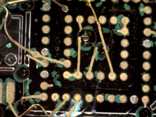
We examine the remains of the footprint on the printed circuit board.

We are delighted by the penetration of the epoxy under the BGA. We see no sign of dendrites. According to this treatise, integrated circuits in plastic packages can suffer damage in high humidity and heat whether they are biased (powered up) or unbiased (no power connected). The biased circuit moisture test performed by Lattice Semiconductor, manufacturer of U8, is to subject the package to 85°C and 85% relative humidity for 1000 hr. In Reliability Technology: Principles and Practice of Failure Prevention in Electronic Systems by Pascoe, the author presents Hallberg and Peck's formula for rate of failure in integrated circuits. The rate is proportional to the third power of relative humidity, and to exp(E/kT) with E = 0.9 eV. Thus 25 years at 20°C and 50% humidity is like 32 days at 60°C and 100% humidity or 6 days at 90°C and 80% humidity. The third conditions caused failures similar to the first condition. Given that U8 can survive 1000 hr at 85% humidity and 85°C, it can endure 4500 hr at 60°C and 100% humidity.
We note, however, that Hallberg and Peck's work does not cover the case where the components are immersed in water. Our test batch is poaching in 100% humidity at 60°C with two quenches in cold water per week, which will cause condensation in all available cavities within the encapsulation. When immersed in water, printed circuit board traces can be joined by dendrites in a few minutes at 85°C. (This video appears to show rapid dendrite formation in hot saline, although we are not certain that it is real-time.)
If we cannot use the absolute formula for time to failure that is provided by Hallberg and Peck, we can use their study of the activation energy of various rate-determining steps in the chemical process that leads to failure. They give this energy as close to 0.9 eV. We refine the calculation we did above, using 310 K for implanted devices and 333 K for our test batch. We get a time to failure 10.3 times longer for implanted than poaching at 60°C. Our first failures occurred after 5 weeks at 60°C, so we expect time to failure while implanted to be closer to 50 weeks.
[16-APR-15] Batch C74.13-C75.9, C75.11-C76.1 has been soaking in water since 13-APR-15. Switching noise is less than 4 μV for all devices and VBAT is 2.55-2.65 V. When measuring frequency response in the Neuroarchiver, we set the default frequency to 256 SPS this time. Frequency response is within 2 dB of nominal for all devices.
[17-APR-15] Test transmitters R72.1, 3, 5-8, and 10 are still running. Battery voltages all normal.
[22-APR-15] We have batch R76, which has been soaking in hot and cold water for four days. Battery voltage 2.58-2.68 V in cold water. Switching noise less than 12 μV. Switching noise less than 5 μV. Frequency response within 1 dB of nominal except R76.8, which is 2 dB above nominal at 130 Hz.
Test transmitters R72.1, 3, 5-8, and 10 are still running. Battery voltages are normal except R72.6, which has dropped to 2.38 V. Gain versus frequency in R72.1 is 3 dB too low at 50 Hz and 6 dB too low at 130 Hz. In R72.5 it is 3 dB too low at all frequencies. The others have gain versus frequency within 2 dB of nominal.
[27-APR-15] Test batch R72.1-10 were put in to poach at 60°C 7 weeks ago today. We are ending the test today, after the equivalent of 70 weeks at 37°C. R72.1 developed reduced input impedance at Week 6. At Week 7 it functions perfectly when driven by a 50-Ω source. Battery voltage 2.8 V. R72.2 developed reduced reduced input impedance at Week 3 and failed by all-zero transmission then battery drain at Week 5. R72.3 develops reduced input impedance at Week 3 and a +10 MHz shift in center frequency at Week 4. This shift reversed after we tore off silicone. We baked until Week 7 and it functions perfectly with battery voltage 3.0 V. R72.4 stopped transmitting at Week 5 and dissection showed excessive current drain. R72.5 developed reduced input impedance at Week 6 and battery voltage has dropped to 2.2 V at Week 7. R72.6 battery drain took place in the days leading up to Week 7. R72.7 we baked the entire seven weeks and is running perfectly still, except for the poor frequency calibration it started with. R72.8 drained its battery some time during Week 7. R72.10 developed reduced input impedance at Week 7.
The reduced input impedance would not affect recordings from 10 kΩ electrode wires or 1 kΩ skull screws. The first significant failure we observe is the temporary frequency shift in R72.3 at Week 4. Battery drain problems start at Week 5. At 37°C we expect our time to first failure in a batch of 10 transmitters to be around 40 weeks, which is longer than the 18-week operating life of the A3028R.
[06-MAY-15] We have batch R77.10-78.9 after a seven-day inactive soak in hot and cold water. Gain versus frequency is within 1.5 dB of nominal for all. Reception is perfect. Battery voltage and noise are normal.
[08-MAY-15] We have batch R76.14-77.9 after a four-day soak with charges of hot water. We turn them all on and place them in water in a faraday enclosure with two pick-up antennas.

The imperfect reception is due to collisions in the small space of the enclosure. When we place the transmitters individually in the enclosure, reception is in every case perfect. We measure gain versus frequency and find it to be within 1 dB of nominal with the correct slump in gain before the bump at 130 Hz.
[11-MAY-15] We put a plastic bin in our FE2A faraday enclosure. We tape a transmitter to a self-propelled ball. Later, we put the ball in a latex glove with the transmitter and allow it to move around in water, like this. We measure reception from one antenna with the lid on and off, for various transmitters, over a one-minute period.
| Device | Lid | Antenna | Reception | Immersed | Leads |
|---|---|---|---|---|---|
| B79.1 | on | 30 mm | 98.3 | no | 100 mm, 1 loose, 1 taped |
| B79.1 | on | 30 mm | 97.1 | no | 100 mm, 2 taped |
| B79.1 | on | 30 mm | 97.9 | no | 100 mm, 2 loose |
| B79.1 | off | 30 mm | 73.3 | no | 100 mm, 2 taped |
| C75.10 | on | 50 mm | 99.1 | no | 45 mm, 2 taped |
| C75.10 | on | 50 mm | 99.0 | no | 45 mm, 2 loose |
| C79.2 | on | 30 mm | 98.8 | no | 45 mm, 2 loose |
| R76.13 | on | 50 mm | 99.1 | no | 150 mm, 2 taped |
| R76.13 | on | 50 mm | 99.1 | yes | 150 mm, 2 taped |
| C75.10 | on | 50 mm | 94.2 | yes | 45 mm, 2 taped |
| B79.1 | on | 30 mm | 97.7 | yes | 100 mm, 2 taped |
| B79.2 | on | 30 mm | 93.4 | yes | 100 mm, 2 taped |
| B79.2 | on | 30 mm | 95.3 | yes | 100 mm, 2 taped |
We measure received power from moving transmitters also. We record the average decibel power measurement (dBm is 10 times log of power divided by 1 mW), min and max power also.
| Device | Antenna | Min Power |
Ave Power |
Max Power |
Immersed |
|---|---|---|---|---|---|
| B79.2 | 30 mm | −61 dBm | −47 dBm | −36 dBm | no |
| B79.2 | 30 mm | −68 dBm | −49 dBm | −34 dBm | no |
| C75.10 | 50 mm | −66 dBm | −47 dBm | −35 dBm | no |
| R76.13 | 50 mm | −68 dBm | −48 dBm | −37 dBm | no |
| R76.13 | 50 mm | −75 dBm | −54 dBm | −39 dBm | no |
| C75.10 | 50 mm | −73 dBm | −57 dBm | −39 dBm | no |
| B79.1 | 30 mm | −75 dBm | −54 dBm | −38 dBm | no |
We see no significant difference in performance between immersed transmitters with the 30-mm and 50-mm antennas. This suggests that we might reduce the length of the mouse transmitter antenna without compromising performance. We see no difference between power received from rat and mouse transmitters, so we still have no explanation for why mouse transmitters perform less well in IVC racks than rat transmitters.
[11-MAY-15] We have test batch B78.10-B79.5. They are all encapsulated with 30-mm antennas. Device B78.13 is running when we receive them for first test. Center frequency is 914-919 MHz. Reception 100% in faraday enclosure for all. Gain versus frequency within 2 dB of nominal. We place in the oven at 60°C in a box for burn-in in dry air.
[12-MAY-15] Eight out of ten transmitters in text batch B78.10-B79.5 are running when we drop them in a pile on our bench antenna. Two are not running. We turn them on. They are B78.10 and B79.4. We place them all in water. At first, battery voltages vary, but after ten minutes we get the following with one antenna in a faraday enclosure.

We take B78.14 out to bring to ION for some tests. We leave the other nine running in water at 60°C.
[18-MAY-15] Batch B78.10-13, B79.1-B79.5 all running fine after one week running poach. We check frequency response, reception, and battery voltage.
[20-MAY-15] Batch B78.10-13, B79.1-B79.5 all running. B79.1 battery voltage is 2.31 V. Others are 2.62-2.69 V. Frequency response of all devices is okay. Center frequencies 915-920 MHz. B79.1 we turn on and off a few times. Its battery voltage remains the same. Return to oven to continue running poach.
[21-MAY-15] Batch B80.1-11, B80.13-14 has passed through 24hr/60°C/D/ON (twenty-four hours at sixty degrees centigrade in dry air, running). Battery voltages are 2.49-2.53 V. Noise is 10 μV. Reception is good. Gain versus frequency close to nominal. We place in water for 72hr/20°C/W/OFF.
[21-MAY-15] Batch B78.10-13, B79.1-B79.5 has been running in water at 60°C for ten days. Two won't turn on: B79.1 and B79.2. The others are still running and battery voltages are normal. We remove silicone from B79.1, cut through positive battery lead, scorch away epoxy around negative battery lead, and connect 2.7 V. The device switches on and off, transmits well, and responds to mains hum. The average value of X varies correctly with VB. Current consumption while running is 370 μV, and when off is 300 μA. Remove C2, active current consumption drops to 80 μA. We expose B79.2 battery terminals and disconnect battery. Its voltage is 2.1 V. Connect 2.7 V. When on, transmitter draws 90-120 μA, varying. When off, 2.1 μA. We turn on and wait ten minutes. Current is stable at 89 μA. No sign of corrosion, leaking, or discoloration of any part of the encapsulation or the leads. We note that scorching off the epoxy and soldering test leads to the battery footprint heats up the entire circuit.
[22-MAY-15] B78.10 has stopped. B79.5 battery voltage 2.14 V. B78.11-13,B79.3-4 have battery 2.54-2.63 V. They pick up mains hum. We expose B79.5's battery terminals. We turn off and measure VB−VC = 2.4 V. We cut battery positive lead and measure VB 2.5 V. We apply 2.6 V. Off current 1.6 μA, on current 81 μA. Expose B78.10 terminals. Cut positive battery lead, measure VB−VC = 1.4 V. Apply 2.6 V. Off current 1.7 μA. On current 1.7 mA. Transmits zeros. We heat up C5 with a soldering iron. On current drops to 90 μA. We raise VB to 4.3 V. On current 104 μA. Drop to 2.6 V, 89 μA. Average X now indicates VB = 2.88 V. No sign of corrosion, leaking, or discoloration of any part of the encapsulation or the leads.
We take a fresh A3028 circuit and calibrate it. We replace C2, C5, and C6 with 100 nF. We solder the X inputs together and measure the following noise spectrum over 16 s.

So far as we can tell, dropping the decoupling capacitance on VB, VA, and VC from 10 μF to 0.1 μF has no affect on the signal noise. Gain versus frequency is within 2 dB of nominal after we wash and dry.
[24-MAY-15] B78.11, B78.12, B79.3 still running with battery voltages 2.58-2.64 V. But B78.13 and B79.4 have stopped. B78.13's battery, when disconnected, is 0.8 V. Inactive current with 2.6 V applied is 1.6 μA and active is 83 μA. Picks up mains hum. Reception is good. B79.4's battery, when disconnected, is 1.7 V. Inactive current when we first apply 2.6 V is 3000 μA, but we disconnect and re-connect and now active current is 89 μA and inactive current is 1.9 μA.
[26-MAY-15] B78.11 battery voltage is now 1.98 V while B78.12 is 2.67 V and B79.3 is 2.65 V. All pick up mains hum. All switch on and off. We strip silicone off B78.11 and measure VB−VC = 0.3 V. We disconnect the battery and apply 2.6 V. Active current 92 μA, inactive 2.1 μA.
[27-MAY-15] Batch B80.1-11, B80.13-14 has been through 120hr/20°C/W/OFF. Transmitters B80.5 and B80.11 have rust around their positive battery terminals, as shown below. We observe the rust re-forming twice, so we are convinced it is not debris in the water.

We observe water leaking out near the positive battery terminal in B80.11. There is one bubble near the positive battery terminal on each of B80.5 and B80.11. The silicone over the corners of the battery terminal is thin in B80.1. B80.5 switching noise is 80 μV, B80.11 switching noise is 40 μV, B80.1 switching noise is 24-μV switching noise and harmonics. Remainder have switching noise less than 3 μV. Battery voltages are 2.53-2.56V. Frequency response of all devices is within 2 dB of nominal. We connect a microammeter to C and a pan of water. We lower the body of the device into water and measure current flowing from the battery positive terminal to V through whatever leak might exist in the silicone coating. The transmitter is off. If there is current, we confirm that it is the corner with the battery terminal that is the source of the connection to the water. We test all devices. B80.1 = 2 μA, B80.5 = 20 μA, B80.11 = 15 μA, all others 0.0 μA.
B78.12 and B79.3 are still running with normal battery voltage.
We have batch B79.6-9, B79.12-B80.4. These were intended to be a batch of A3028Rs, but we left them soaking in water for five days and we now find there is white residue around the logic chip. We decide to replace the 10-μF capacitors with 1-μF capacitors and load mouse batteries to see if we can get longer life with the smaller capacitors.
[28-MAY-15] Batch B80.1-11, B80.13-14 now has two extra coats of silicone over the positive battery terminals. We measure battery leakage through encapsulation and find it 0.0 μA for all devices. Noise in B80.1 is 9 μV rms, in B80.5 is 12 μ, and in B80.11 is 8 μV.
B78.12 still running with normal battery voltage, but B79.3 has died. Its battery voltage is 2.4 V. Inactive current is 1.7 μA. Active current is 4 mA and we get reception. We remove C4. Active current is 3 mA and we have no reception. We re-connect power and active current is 100 μA but no reception. We replace C4. Active current 93 μA and good reception.
[29-MAY-15] B78.12 still running with VB = 2.7 V. Noise is 24 μV. Switching noise is 8 μV.
[01-JUN-15] B78.12 still running with VB = 2.65 V. Noise is 14 μV. Reception and frequency response are normal. Today is its 19th day poaching.
[03-JUN-15] B78.12 still running with VB = 2.43 V. Noise is 16 μV rms.
[04-JUN-15] B78.12 has expired after 23 days running at 60°C in water. We write this e-mail summarizing our reliability studies.
[05-JUN-15] We have B79.6-9,B79.12 with 1-μF capacitors in place of C2, C4, C5, C6, and C8. batteries loaded. We have B79.13-B80.2 with the 10-μF capacitors intact. These are protected-input circuits on the A302801D circuit board. We load 48 mA-hr batteries. Three of them, B79.9, B79.12, and B80.1 won't turn on, although they worked when powered earlier in the day from the programming extension. We observe dendrite growth between U1-1 and U1-2, which turns off the U1-1 mostfet so VM is disconnected from VB. No power reaches the circuit.

We scrub the boards and dry in hot air. All three of them now work well, picking up mains hum and giving good reception.

We inspect the remaining circuits, and they too have corrosion and dendrite growth around U1-1 and U1-2. But there is no connection between the pads yet.
[18-JUN-15] We hear of the sudden failure of R69.3 at Marburg, in archive M1434591227.ndf. Reception starts to degrade at 3:39:47. By 3:39:50 reception has stopped. We are back to 100% reception at 3:40:03. From there, reception is close to 100%, with stable battery voltage until 3:49:51, when reception drops to 0% from one sample to the next, with no change in battery voltage in the final moments.
[23-JUN-15] Test batch No79 consists of transmitters B79.6-9,12-14, B80.1-2. Transmitters B79.6-9, 12 we equipped with 1-μF in place of C2, C4, C5, C6, and C8. The remainder are control circuits with 10 μF in these locations. The circuit boards are A302801D input-protected circuits with mouse batteries loaded, to make something equivalent to the A3028B, but looking as below.

The protruding battery battery contacts will allow us to gain access to the battery terminals without having to heat up the capacitors on the circuit. B79.7 fails after encapsulation. The remaining eight survive burn-in 24hr/60°C/D/ON. We measure noise in water less than 12 μV and reception is perfect. Center frequencies are around 915 MHz. Frequency response within 2 dB of nominal except No79.6 and No79.8 which show +3 dB at 130 Hz. Note that in B79.6, B79.8, B79.9, and B79.12 we have C8=1μF and R6=50kΩ, which gives the transmitters a high-pass response with half-power frequency 3 Hz. The other four have low-frequency cut-off at 0.3 Hz. The difference in their response is clear in the first few oscillations of our 1-500 Hz sweep. We turn them all on and put them in the oven to poach in water at 60°C.
[24-JUN-15] ION measures reception in an IVC rack isolation chamber. They arrange four antennas around four mouse cages, each with a mouse and A3028B transmitter. Two other cages are on the far edges of the rack. They measure reception during four hours with an Antenna Combiner (A3021B) and Data Receiver (A3018D) and then for four hours with an Octal Data Receiver (A3027D).
| No | A3021B+A3018D | A3027D | Comment |
|---|---|---|---|
| 4 | 94.7 | 97.0 | Near |
| 6 | 78.1 | 98.3 | Far |
| 9 | 96.6 | 98.8 | Near |
| 12 | 97.7 | 96.7 | Near |
| 13 | 97.4 | 99.4 | Near |
| 14 | 80.2 | 98.2 | Far |
We still have not figured out why mouse transmitters performed less well than rat transmitters in ION's original IVC rack enclosure, when a 20-cm gap was present in the back corner. But we see that reception from these transmitters is excellent in the new enclosure without gaps.
[25-JUN-15] Transmitter B82.4 has a 30-mm antenna. We place it on out spectrometer antenna and measure peak power −29 dBm at 915 MHz. We place it in a petri dish of water in the same location and get −39 dBm.
Batch B82.4-14 have endured 24hr/60°C/D/ON. Frequency response is within 2 dB of nominal for all. Battery voltages 2.51-2.66 V. Noise below 15 μV. Reception robust. Turn them all off and put them in water at room temperature.
Test batch No79 all eight running, battery voltages 2.64-2.73 V. Reception from jar is good after cooling down. Return to oven to continue poach.
[29-JUN-15] Batch B82.4-14 has endured 96hr/20°C/W/OFF. Frequency response within 2 dB of nominal, battery voltages 2.48-2.62 V, noise below 15 μV, reception robust. Turn them all off and dry them ready to ship.
Test batch No79 all eight running. Battery voltages 2.67-2.75 V. Noise less than 15 μV except B79.8, which has noise 35 μV in repeated measurements. The noise spectrum of all eight transmitters is here. B79.8's noise appears to be switching noise plus some higher-frequency noise similar to what we see when the 0-V wire breaks. We measure frequency response. All within 2 dB of nominal except B79.8 has gain 3 dB above nominal at 130 Hz. Reception is robust for all. All are running when we return them to 60°C poach.
[01-JUL-15] Test Batch No79, eight transmitters still running, battery voltages 2.64-2.74 V.
[02-JUL-15] Test Batch No79, eight transmitters still running, battery voltages 2.67-2.74 V.
[03-JUL-15] Test Batch No79, eight transmitters still running, battery voltages 2.63-2.68 V.
[04-JUL-15] Test Batch No79, eight transmitters still running. B79.8 has 20-mV 195-Hz oscillation that we cannot stop even by shorting X leads together, reception perfect. B79.2, B79.6, B79.9, B79.12, B79.13, B79.14 gain versus frequency within 2 dB of nominal, reception perfect. B80.1 gain is 3 dB too high at all frequencies, reception perfect. Battery voltages 2.64-2.72 V for all. Noise less than 20 μV in all but B79.8. Turn them all on and continue the poach.
[06-JUL-15] Test Batch No79, eight transmitters still running. Battery voltages 2.64-2.72 V after a few minutes settling at 20°C. During settling, No79.13 shows jumps of order 1 kcount and No80.2 of order 100 counts.
[08-JUL-15] Test Batch No79, eight transmitter still running. Average value of B79.12 starts off at 51 kcount and drops over twenty minutes to 46 kcount. During this time, the oscillations on B79.8 diminish and vanish over a one-minute period. We now get the following.
ID (No) RECEPTION (%) VA (V) NOISE (uV rms)
1 98.83 2.66 9.96
2 94.34 2.71 40.36
6 98.83 2.64 18.48
8 96.29 2.53 35.36
9 90.62 2.64 18.20
12 99.80 2.56 18.68
13 99.41 2.69 7.96
14 80.66 2.67 9.52
Batch R83.2-12 endured 24hr/60°C/W/ON. All are fine afterwards except R83.4, which won't turn on or off. Turn them all off and put them in water to soak.
[10-JUL-15] Test Batch No79, eight transmitters still running. We put them in 20°C water. B79.6 noise 15 μV, VBAT = 2.6 V. B79.8 oscillating initially, but settles down to 150 μV noise and VBAT = 2.4 V. B79.9 noise 25 μV, VBAT = 2.3 V. B79.12 oscillating full-scale at 160 Hz. B79.13 occasional 10-mV swings. Otherwise battery voltage appears to be 2.6 V. B79.14 shows occasional 10-mV swings. Otherwise battery voltage appears to be 2.6 V. B80.1 shows occasional 10-mV swings. Otherwise, battery voltage appears to be 2.6 V. B80.2 shows occasional 10-mV swings about a baseline. Battery voltage appears to be 2.1 V.
[11-JUL-15] Test Batch No79, seven transmitters still running, B80.2 won't turn on. Battery voltages and noise are as shown below. B79.12 is still oscillating at 160 Hz.
ID (No) RECEPTION (%) VA (V) NOISE (uV rms)
1 97.46 2.64 12.00
6 97.46 2.64 19.88
8 99.80 2.20 257.56
9 99.02 2.61 19.12
12 100.00 2.67 5619.84
13 94.92 2.70 16.84
14 94.92 2.63 17.76
We measure current consumption of a bare A3028A circuit with input leads shorted together and get 90 μA. We connect 100 mVpp, 100 Hz and get 95 μA. With 100 mVpp, 10 Hz, 94 μA. With 1 Vpp, 100 Hz we get 94 μA. Back to inputs shorted we get 89 μA.
[13-JUL-15] We have batch R83.2-12. Of these, R83.4 already failures during burn-in. After 6days/20°C/W/OFF the ten remaining have gain versus frequency within 2 dB of nominal. Noise and reception simultaneously in water are as follows.
ID (No) RECEPTION (%) VA (V) NOISE (uV rms)
2 48.83 2.66 11.08
3 50.00 2.67 8.36
5 48.63 2.63 11.76
6 48.05 2.70 14.40
7 48.63 2.67 12.44
8 48.05 2.68 16.24
9 50.00 2.70 10.96
10 45.51 2.68 10.32
11 49.80 2.65 15.08
12 48.24 2.67 13.56
Test Batch No79, seven transmitters still running. R79.6 gain versus frequency has nominal shape but is 2 dB too low throughout. R79.8 still oscillating at 160 Hz. R79.9 baseline swings and noise. Gain has correct shape but is 6 dB too low. R79.12 gain is 10 dB too low and when in water we see spiky noise of 7-15 Hz, usually around 10 Hz, as shown below.

R79.13 gain is 6 dB too low. R79.14 and R80.1 gain is within 2 dB of nominal. Battery voltages are 2.46-2.70 V.
[15-JUL-15] Test Batch No79, two transmitters still running. B79.8, B79.9, B79.12, B79.14, and B80.1 won't turn on. B79.6 battery voltage now around 2.3 V but it picks up mains hum just fine. B79.13 still has lots of low-frequency noise and rumble. Battery voltage appears to be around 2.7 V. We turn off the transmitter, remove silicone and measure battery voltage directly as 2.7 V. We put B79.13 in the oven. After an hour, noise is gone, gain is 6 dB too low but otherwise looks good.
Test Batch No79 Summary: These eight transmitters were built with the A3028R1 protected-input circuit, built with lead-free solder in January 2015, and loaded with 48 mA-hr batteries. Expected operating life is 21 days. All eight suffered corrosion of joints when left in water for several days. We expected problems with the EEG amplifier as a result, but our objective was to look for failure in the 1-μF and 10-μF capacitors. Four had 1-μF capacitors in place of 10-μF. Of these four, all ran for at least 21 days. One developed oscillations in its amplifier and another showed loss of gain. Of the four with 10-μF capacitors, one failed after 18 days. The others ran for over 21 days.
[16-JUL-15] We are having trouble with the P3028A05 firmware. Once again, the problem arises with frequency_low = 7, as we observed with firmare 4 and 5, and which we believed we had fixed in 6. We note that the TCK period is not increasing linearly with fast clock divisor, and from 13 to 14 it actually decreases. In our P3030D07.vhdl firmware, we discovered that the failure of the fast clock divisor was the result of the ring oscillator being too fast. We add another gate to the ring oscillator, so it now has three gates and a frequency of around 100 MHz. At this lower speed, the clock divider is stable, and we obtain the following encouraging plot of TCK period versus fck_divisor.

The transmit clock (TCK) generation is well-behaved, but the problem with frequency_low = 7 persists.
[29-JUL-15] In the A06 firmware, we declare signal FHI as a pin with no assigned location. This is a bug we introduced in A06 as we were trying to fix another bug. If we make FHI a node that we keep, the problem with frequency_low stops. But we still have glitches on FHI so we replace it with BIT, which we keep as a node so as to simplify the calculation of F1..F4. If we don't keep BIT then F3 comes out wrong for frequency_low = 7 and x_id = 7 with version = 1. We re-program 14 A3028B circuits with this new code, P3028A07. The average current consumption without antenna drops from 85.8 μA to 78.9 μA, which for the A3028B means expected battery life rises from 559 hours to 608 hours.
[31-JUL-15] We take an A3028D and replace all its 10-μF capacitors with 2.2 μF. We set R6 = R13 = 249 kΩ, R7 = R14 = 10 MΩ, and C9 = C14 = 220 pF. We measure gain versus frequency for both X and Y.
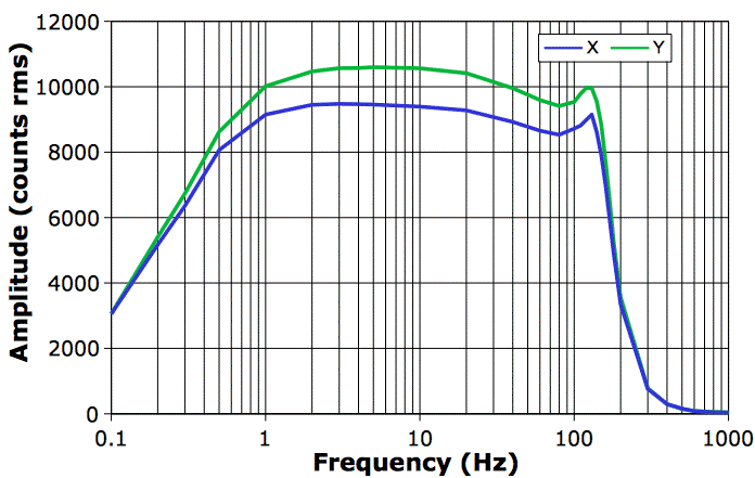
We increase R6 and R13 from 50 kΩ to 249 kΩ so as to keep the time constants R6C9 and R13C14 at 0.5 s. We increase R7 and R14 from 2 MΩ to 10 MΩ so as to keep the gain of the first amplifier stages at ×40. Ideally, we would drop C9 and C14 from 1 nF to 200 pF to keep the time constants R7C9 and R14C14 at 10 ms. But we don't have 200 pF so we use 220 pF instead. One concern we have about moving from 10 μF down to 2.2 μF is noise on the inputs from poorly-decoupled power supplies. When placed in a faraday enclosure with inputs connected by 20 MΩ, we see 36 counts of noise, or 14 μV.
We have batch B84.1-14, all with 30-mm antennas, our new standard. After epoxy, B84.9 will not turn on, but battery voltage is 3.0V. After encapsulation, frequency response of the remaining circuits is within 2 dB of nominal. Reception is 100%.
[10-AUG-15] Batch B84 has endured 2hr/60°C/D/ON and 72hr/20°C/W/OFF. Frequency response is within 2 dB of nominal, reception is 99% or higher, battery voltages 2.51-2.51V, noise around 12 μV.
We inspect a B85.9, which failed after loading the battery, and find that the positive battery terminal is not soldered. We solder the terminal and the transmitter now turns on and off, has good reception and nominal frequency response. We inspect B84.9, which failed after encapsulation. We remove epoxy from the positive battery terminal and find it is not soldered. We solder it and the transmitter now turns on and off, has good reception, and nominal frequency response. We have one bare A3028R1 assembly that won't turn on and one A3028AV3 assembly that won't turn on. We find that U3 is not responding. We cannot remove U3 by heating, so we tear it off another board without heating first, so as to make sure the underneath is clean. We get this photograph of the underside, in which the PCB tracks have adhered to five of the pads, but not to U3-2, which will give rise to failure to turn on and off. Beneath the one we heated, we have a sticky mess, which might be dried out flux.
[12-AUG-15] We hear from our assembly house that U3 would be better soldered with their My600 paste printer. We also resolve to ask for leaded assembly rather than unleaded.
We have batch B85.1-14. Of these, B85.9 failed because its battery tab was not soldered, B85.14 failed for some unknown reason because we can't find it to test it, and the remainder have endured 2hr/60°C/D/ON and 72hr/20°C/W/OFF. Frequency response is within 2 dB of nominal. Reception is 99% or higher. Battery voltage 2.52-2.61 V, noise around 10 μV in water.
[04-SEP-15] We have 40 of the new A3028AV4, following the A3028D_1 schematic, with 2.2-μF automotive-grade capacitors (in place of 10-μF general-purpose) and leaded solder (instead of lead-free, as we called for in the A3028AV1-3). We measure gain versus frequency for X input and find it within 1 dB of nominal. We obtain this plot of period versus divisor. The ring oscillator is running at around 73 MHz, compared to 92 MHz for the V3 hardware.
[08-SEP-15] We are working on a depth electrode for Iris Oren, which we will call Electrode H. The idea is to solder the EEG lead directly to a teflon-insulated, platinum-indium electrode wire, at a 90° angle. The implanter will cut the Pt-In wire to the desired length. A holder attached to the electrode allows us to raise and lower it until it is located correctly. We cement the electrode in place, then remove the holder. The figure below shows our prototype, in which we have soldered three wires together, one Pt-In 125-μm diameter insulated with 200-μm diameter teflon, one stainless steel helix in red silicone, and one 260-μm diameter tinned copper wire in 530-μm PVC. The copper wire runs up through a blunt-ended syringe needle. When it emerges from the plastic syringe lock, we bend the wire and hold it in place with aluminum tape.

The implanter can hold the electrode by the syringe lock, and so manipulate it precisely during implantation. Cement will cover the solder joint, but not the tip of the syringe needle. After the cement has set, the implanter cuts the bend in the wire within the plastic syringe lock, and pulls the syringe needle away, leaving a length of copper wire behind.

The implanter cuts the copper wire off flush with the cement, and covers with another layer to insulate the exposed copper.
[08-SEP-15] We have B85.9, B86.1-8 after three-day soak in water. Battery voltages from average signal value are 2.47-2.53V. Frequency response is within 2 dB of nominal. We have old transmitters A64.1, 3, 5, 7. Battery voltage for A64.1, 5, 7 are around 2.6 V, but A64.3 won't turn on. Reception and mains hum pick-up. Gain versus frequency for both channels of A64.1, 5, 7 all within 2 dB of nominal. Transmitter F66.7 battery voltage 2.5 V, gain versus frequency within 2 dB of nominal, bandwidth 0.3-320 Hz. We open the A64.3 up and find the battery is drained. Current consumption with 2.9 V supply is 1.8 μV when asleep and 149 μV when active. We get perfect
[11-SEP-15] We take an A3028AV4 circuit with its 0.3-160 Hz amplifier and program it to transmit 128 SPS on both channels. We encapsulate in epoxy without a battery, with the help of a crude rotator. We call this device TX1.1

Transmitter TX1.1 has life 950 hours with a 48 mA-hr battery. If ten transmitters survive in 100% humidity at 60°C for 950 hours with such a battery, we figure their chance of failure in one year at 37°C will be less than 10%.
[15-SEP-15] Transmitter TX1.1 below is encapsulated in epoxy only.

We deliver power through a microammeter. We measure current consumption as we lower the device into water all the way up to the programming extension.

The encapsulation appears to be water-proof. We enclose the transmitter and leads in water inside the finger of a latex glove, and tighten the seal around the programming extension with some silicone tube. We connect a 48-mA-hr battery to the extension, turn the transmitter on, and place in a faraday enclosure jar inside our 60°C oven to poach.
[22-SEP-15] We have batch 1176B consisting of B86.4-5, B86.10-14, B87.2-3, B87.6. Frequency response is within 2 dB of nominal. Reception perfect. Below is reception, battery voltage, and noise for all of them running in water on an antenna.
ID RECEPTION VA NOISE
2 96.29 2.51 10.16
3 99.22 2.52 8.24
4 98.63 2.53 9.28
5 99.02 2.56 8.16
6 98.63 2.52 9.92
10 97.46 2.54 9.52
11 93.16 2.52 7.84
12 98.05 2.51 9.32
13 96.09 2.51 11.68
14 90.23 2.53 9.88
We have E87.7 with water-soluble flux on its components. We turn on with external battery. We observe a 1-Hz full-scale square wave. We wash and blow dry. No more square wave, frequency response within 2 dB of nominal.
We remove TX1.1 from the oven. Our latex water reservoir still contains water, but the jar outside has water condensation all around the walls. There is corrosion between the pins of P2. The battery is drained. We clean and dry the circuit. Current consumption is 2.1 μA when inactive and 54 μA when active. Reception is good, frequency response correct. The electrode solder joints are corroded in a way we do not observe when we poach fully-encapsulated transmitters, see here. The gold pins, gold pads, steel screw, and steel wires show no signs of corrosion. The epoxy encapsulation appears to be unaffected by the poach.
We place the circuit in a zip-lock plastic bag, within a beaker wrapped in foil. We place the apparatus in our oven and tape steel mesh over the window to stop signal getting out. We leave the circuit to poach.

The above arrangement keeps TX1.1 in 100% humidity, but as the water evaporates and escapes through the bag, the device will not be immersed in water. Nevertheless, we trust that the saturated environment will be similar to the one encountered by epoxy coated with silicone inside an animal.
[25-SEP-15] We remove TX1.1 from the oven and blow it dry. Inactive current is 1.9 μA. We switch on and current rises as shown below.

[28-SEP-15] Transmitter TX1.1 operating current is 66.5 μA after one minute settling. Gain versus frequency is within 2 dB of nominal (note that this circuit has low-pass filter 160 Hz but sample rate only 128 SPS so we see aliasing at 64 Hz. Battery voltage is 2.66 V with the BR1225 we have been using in the oven.
[29-SEP-15] At first, TX1.1's operating current is 75μA. We scrub, wash, and dry its programming extension. Operating current is now 57.0 μA after one minute, and sleep current is 1.9 μA.
[30-SEP-15] Batch 1177, consisting of E87.7-88.5 made with A3028AV4 circuit, has been through 8hr/60C/D/ON and 40hr/20C/W/OFF. Gain versus frequency is within 2 dB of nominal. Noise is less than 12 μV. Reception is perfect. Battery voltages 2.55-2.66 V. Transmitter TX1.1's operating current is 55 μA immediately after activation, but rises to 57 μA after a few minutes.
[02-OCT-15] Batch 1181 consists of E89.1-14 made with A3028AV4 circuits. We turn them all on and place them in a box on an antenna to pick up mains hum. We measure battery voltage, reception, and signal amplitude. We place in a faraday enclosure with the lid off and do the same measurement. We put the lid on and do the same again.
| Location | Reception (%) | VB (V) | Amplitude (counts) |
|---|---|---|---|
| Bench | 91.5 | 2.75 | 2228 |
| Enclosure, Lid Off | 94.4 | 2.76 | 42 |
| Enclosure, Lid On | 92.9 | 2.79 | 32 |
We place the batch in the oven to burn in at 9:36 am. We have R88.7-10 made with A3028RV1 circuits. We turn these on and reception, battery voltage, and noise look fine. We put them in the oven to burn in as well.
Transmitter TX1.1 operating current is 64.3 μA immediately after activation, rising to 66.5 μA after five minutes. Inactive current is 1.9 μA. Transmitter E88.5 is fully encapsulated, made from the A3028AV4 circuit and has been running in 60°C water since 12 pm 30-SEP-15. Battery voltage is 2.70 V.
[06-OCT-15] Transmitter TX1.1's BR1225 battery is drained to 0.5 V. It has been running in water since 15-SEP-15. We last checked on it 02-OCT-15. Operating current is 61.1 μA five minutes after turning on. When we connect a new battery, the average value of X is 42.6k and of Y is 37.2k. Frequency response within 2 dB of nominal. We connect a 1000 mA-hr battery and put TX1.1 back in the oven to continue poaching. A few hours later, we measure average X 42.5k and Y 39.9k. E88.5 running fine, battery voltage 2.7 V.
Batch 1403R R88.7-88.10 have done burn-in and soak, all four are fine. These are replacements for job 1403 failures. Batch 1181 E89.1-14 bave done burn-in and soak. All fourteen are fine: frequency response, battery voltage, reception, and noise.
We have R68.8, R68.9, and R69.3 returned from Marburg. R68.8 consumes over 2 Amps, and C2 starts to smoke. There is green residue around the ends of C2 and C5. We remove C2 and C5. Current consumption is 55 μA. We get no reception. We attempt to replace C2 and C5 but tear off a pad and abandon the effort. R68.9 battery is drained. When on, the circuit consumes only 53 μA. We get no reception. We replace C2 and C5. Current is 70 μA and we see mains hum transmission. After a few minutes, current consumption drops to 52 μA and transmission stops. R69.3's battery is drained. We connect external power. Current consumption is 86 μA. Frequency response is within 2 dB of nominal. Reception perfect.
[09-OCT-15] We remove TX1.1 from the oven. It has drained its 1000 mA-hr battery. Current consumption is 1.8 μA when inactive. When active, current starts at 17 mA and drops after a few minutes to 11 mA. We remove C4, C1, and C3. Active current remains 11 mA. The short circuit is something other than a capacitor, and became permanent after 25 days immersed in water with epoxy-only encapsulation. Transmitter E88.5 continues to run in water at 60°C. Battery voltage is 2.7 V, noise 11 μV, frequency response within 2 dB of nominal.
We add to our poach test two further A3028E transmitter made with the AV4 circuit. They are E89.1 and E89.2. We use our new Function Generator (A3031) and Function_Generator Tool to measure and record the frequency response of both devices, and E88.5 as well.
We receive recordings made from an A3028A-HCC at Edinburgh University. Their mouse recordings are now free of the sudden step artifacts they were observing with their earlier depth electrode assemblies. The trace below is a typical recording from the depth electrode and a screw.

Instead of the sharp step artifacts, we see bumps in the data, like the one shown below. It's not clear to us if these are neurological or movement artifact of some sort.

These bumps we can distinguish from seizures and oscillations, so we consider these recordings to be a success.
[13-OCT-15] We take E89.1, E89.2, and E88.5 out of the oven. Battery voltages are all three exactly 2.71 V. Frequency response within 1 dB of previous measurements.
[16-OCT-15] Transmitter E90.9 failed during 24/60°C/D/ON burn-in. This transmitter is built with the A3028AV3 circuit. We dissect the transmitter. Battery voltage is 0.8 V. Inactive current is 1.6 μA. Active current is 2.5 mA. Reception perfect. We pick up mains hum. We remove C2 and C5. Active current is 160 mA. We remove C6 and C4, but active current remains 160 mA. We damaged something. Original symptom consistent with failure of 10-μF capacitor C6.
Transmitters E88.5, E89.1, and E89.2 still running. Reception perfect for all. Battery voltages 2.68V, 2.73V, and 2.29V respectively. Frequency response within 2 dB of nominal. We are about to put them back in the oven when we note that E88.5 is transmitting only value 65535 at 512 SPS. We can get it to transmit other values if we shake it around. We turn them all on and put them back in the oven to poach. Plot E88.5 below shows E88.5's frequency response over the course of two weeks of poaching.
[20-OCT-15] Transmitter E88.5 no longer transmits. This device was performing well until it failed during handling on day 17. Battery voltage 0.8 V. Inactive current 1.7 μA. Active current erratic, starting at 3 mA, fluctuating, dropping as low as 150 μA on occasion. Reception is good. With leads connected, average signal value is correct. Remove C6, C4, C5, C3 and current still fluctuates. Transmitters E89.1 and E89.2 performing perfectly. Graphs of their frequency response versus time are E89.1 and E89.2.
Batch E90.1-14 has been burned in for 24 hours and soaked for 4 days. Transmitter E90.9 failed during burn-in. Transmitter E90.14 has a fine 80-Hz cut-off frequency, see E90.14, which means we must have used an 80-Hz EEG amplifier circuit by mistake. All others, gain within &plusnm; 1 dB range, as shown below. battery voltage from 2.58-2.71, noise below 12 μV, reception perfect.

We add E90.14 to our reliability tests, turning it on and placing it in the oven to poach with E89.1 and E89.2.
[23-OCT-15] We take out E89.1 and E89.2. We notice E89.2 average value is high, while E89.1 is correct. Soon after E89.2's average value is correct. We obtain fine frequency response from E89.1 and E89.2. After a few minutes, E89.1 and E89.2 average values start to jump around. We dissect E89.1. Battery voltage 2.8 V. Active current is 1.5 mA. We remove C6, C4, and then C5. After removing C5, active current drops to 80 μA, but later jumps up to 6 mA. Inactive current is 1.6 μA. We load fresh capacitors in place of C6, C4, and C5. Current consumption is now stable at 100 μA. We wash and dry, re-connect battery. Average value of X is stable at 42 kcount. Frequency response within 2 dB of nominal. We dissect E89.2. Battery voltage is 2.7 V. Active current 80 μA. We apply 2.6 V, but average value of X is 53 kcounts, implying battery voltage of 2.2 V. We replace capacitor C5 and average value is now 45 kcounts. We measure the resistance of the original C5 after wash and dry, and find it to be at least 40 MΩ. Re-connect battery to E89.2 and frequency response is within 2 dB of nominal.
Comparison of V3 and V4 Capacitors: Transmitters E89.1 and E89.2 suffered capacitor failure after 14 days poaching, although they were still transmitting. We suspect that E88.5 suffered capacitor failure also. TX1.1 failed by some other means after 25 days, but was encapsulated only in epoxy. The 10-μF, 10-V, P0402, general-purpose capacitor by Samsung (CL05A106MP5NUNC, $0.30 each) we used in the V3 circuits survived at least 35 days with rat batteries (8 devices), and at least 9 days with mouse batteries (17 devices). The 2.2-μF, 10-V, P0402, automotive capacitor by Taiyo Yuden (LMK105ABJ225MVHF, $0.15 each) provides a minimum of 14 days of operating life for any battery before any sign of damage (3 devices). All three of these devices failed immediately after we transferred them from water at 60°C to cold tap water at roughly 15°C. In Cracks: The Hidden Defect we read, "An assembly should be allowed to cool to less than 6O¡C before it is subjected to the cleaning process." Epoxy has a thermal expansion coefficient of 50 ppm/°C, while the ceramic dielectric used in capacitors has expansion coefficient a little under 10 ppm/°C. If the epoxy cools first by 40°C, we will have a 0.2% strain upon the outside of the capacitor. Until now, we have not kept track of or controlled the way we cool transmitters when we remove them from the oven to test them.
Alternate Capacitor: The 2.2 μF, 35 V, P0402, general-purpose capacitor by TDK (C1005JB1V225K050BC $0.14). The higher voltage rating we assume implies a larger gap between the plates, which may give us more immunity to corrosion.
[25-OCT-15] We remove E90.14 from the oven and let it sit in its hot water in a faraday enclosure. Reception is intermittent (center frequency drops by 0.4 MHz/°C, so at 60°C center frequency is around 900 MHz, too low for reliable reception). But we see enough to measure battery voltage 2.8 V and noise 6 μV.
[27-OCT-15] Transmitter E90.14 VB = 2.66 V, noise 7 μV, reception 100%.
[30-OCT-15] We have batch E92.1-14 after 24hr/60°C/D/ON. Check battery voltages and reception. All good except E92.8, which has average signal value 49k, implying battery voltage 2.4 V. We remove silicone and epoxy to measure battery voltage, and find 2.66 V. A few minutes later, average value is 52k, but we measure 2.62V. We disconnect battery and measure active current consumption 86 μA, inactive 1.7 μA. If the input offset voltage of U5 is 10 mV on each op-amp, we could have an offset as great as 10 + 2.5 × 10 = 35 mV at U5-1. The average signal value would be 1.835 V, and battery voltage would appear to be 0.05 V too low. Transmitter E90.14 VB = 2.79 V, noise 6 μV, reception 100%.
[04-NOV-15] Transmitter E90.14 VB = 2.79 V, reception 100%, frequency response within ±0.2 dB of 20-OCT-15 measurements in the pass-band 1-80 Hz. We have batch E92.1-14, minut E92.8. Reception is 100% for all. We now find that E92.6 has average value 2.5 kcounts. When we apply large mains hum, we see 60 Hz in X, but we cannot measure a frequency sweep. Reception is 100%. For the remaining 12 devices, frequency response within ±0.8 dB as a group, see here. We dissect E92.6 and find that VCOM is around 0.2 V. Soon after removing epoxy around C6, VCOM jumps to 1.8 V. Current consumption around 90 μA. We did not measure current consumption before we started heating C6. We take out E92.8. We have VCOM = 1.8 V, but U5-7 quiescent value is 2.08, while a 10-MΩ probe grounded to 0V records 1.84 V on U5-6. The triangle wave on VA due to sampling is 34 mVpp. We connect ground of our probe to VCOM on C6 and measure voltages with respect to VCOM. At U5-5 we have 0 mV. At U5-6 we have 4 mV. At U5-7 we have 2000 mV. The offset voltage of U5 appears to be 5 mV, while C6 must be short-circuit. We remove C8 and average voltage drops to normal for VB = 2.6 V. We load a fresh 2.2-μF capacitor in C8. We wash and dry. Average voltage on U5-7 is now 6 mV and on U5-1 is 25 mV. We measure VA = 2.56 V. We expect average X to be 65536 × 1.825 / 2.56 = 46.7 kcounts. We observe 46.4 kcounts.
We have batch E93.1-14 not encapsulated. We connect external 2.6-V power and measure TCK period, center frequency, average X (put leads in beaker of water to suppress mains hum), active and inactive current consumption. All are fine.
We have R77.9 returned from the field, where it failed before implantation. Battery voltage is 0.6 V. We destroy the pad around the 0V battery connection, so further diagnosis impossible.
We work on the P3028A09 firmware, after encountering an AV4 circuit that would give TCK period 193 ns or 220 ns, but nothing in between. In the firmware, we take the fck_divisor constant and use it to configure the length of the ring oscillator and the oscillator divisor. The TCK period is proportional to the product of the length and divisor. In the AV4, the constant of proportionality is 9.3 ns, which is two internal gate delays. We attempt to pick length and divisor so that their product is equal to fck_divisor, but we cannot do this when fck_divisor is prime, nor do we support lengths greater than 11 or less than 2. To get a period of 200 ns, we need fck_divisor 21 or 22. We get 21 with divisor/length 3/7 or 7/3, which both give 194 ns. We get 22 with 2/11, which is why we support ring lengths up to 11. With the 11-gate ring oscillator, the code takes 57 of the available 64 outputs in the logic chip. We obtain this graph of TCK period versus fck_divisor shown below.

The troublesome AV4 circuit now gives 194, 202, and 223 ns period for fck_divisor 21, 22, 24. The 11-gate ring oscillator provides the division by 22, which sets the period between the values 194 and 223 ns, which we obtained in the V7 firmware with divisor 7×3 and 8×3 respectively.
[06-NOV-15] Transmitter E90.14 VB = 2.76 V half an hour after being removed from the oven, but still in its warm water, with noise 6 μV and reception 100%.
[10-NOV-15] Transmitter E90.14 VB = 2.3 V after cooling down. Gain versus frequency 0.8 dB higher, although we do see signs of saturation on the top side of the sinusoidal waves. Reception perfect. Noise 20 μV as signal drifts. Once it's at 60°C again in water, battery voltage appears to be 2.5 V.
We set up the apparatus shown below. Transmitter R76.13 sits in a beaker of water. It is running. We apply 2-V 20-ms pulses at 10 Hz to its input. We cover the beaker with a latex glove. In one finger of the glove is a 10-Ω power resistor. We apply 10 V to the resistor.

The beaker will lose most of its heat by radiation, and water is a opaque at infra-red wavelengths. We calculate that 10 W of heat from the resistor should lead to equilibrium at about 60°C. An A3028R should run for 5 weeks at 60°C in water. We will see if the device fails earlier than it should. We set up a computer to record the signal from the transmitter.
[16-NOV-15] Transmitter E90.14 battery voltage 2.6 V, 100% reception after fifteen minutes cooling in its water. We end the R76.13 pulsed poach test. Lots of rust in the water from the alligator clips, and water got through the latex glove to the heating resistor. The water is at 38°C. The transmitter is running perfectly. We turn it off and consider what to do next.
[17-NOV-15] Transmitter B71.7 would not turn on before implantation at ION. The internal circuit is A3028AV3. We perform autopsy. Battery voltage 200 mV. Disconnect battery and supply 2.6 V, active current 160 mA. Clear epoxy from around C2 and C5 (see here), 154 mA. Remove C5, 153 mA. Replace C5, 118 mA. Clear epoxy around C4, 124 mA. Remove C4, 137 mA. Replace C4, 137 mA. Remove C3, 135 mA. This failure is not a capacitor.
We have this this plot of the evolution of the frequency response of E90.14 over the past 27 days poaching. The gain is dropping because the average value of X is around 57k during the sweep. The apparent battery voltage is 2.1 V, which is too low for the circuit to operate. We get 100% reception and 10 μV noise.
We receive 50 of A3028AV5 circuits assembled, as S3028E, with X amplifier 0.3-160 Hz and Y amplifier 0.3-80 Hz. These are made with the MY600 solder paste printer and a covalent-solvent wash (or no-clean process, as they call it.) Our hope is that there will be no ionic residue under U1 and U3 with this process. The big capacitors are 10 μF, 6.3 V, 20% by TDK (445-8920-1-ND). We measure the following frequency response for both channels.

We prepare firmware P3028A10, in which device version 8 configures the circuit to transmit on one channel using the Y amplifier. We will use this firmware to make A3028C circuits. The EEG leads will be yellow and blue.
Batch E93.1-14 has endured 24hr/60C/D/ON and 96hr/20C/W/OFF. Reception is 100% from all devices, battery voltages 2.62-2.70V. Gain versus frequency as shown here. We take E93.2 and E93.9, turn them on, and put them in the oven to poach until failure.
[20-NOV-15] We remove our three poaching transmitters from the oven, but do not take them out of their water. Transmitter E90.14 has apparent battery voltage 2.2 V, but is running well. Transmitters E93.2 and E93.9 have apparent battery voltage 2.7 V.
[23-NOV-15] We take out Transmitter E90.14 but get no reception from it at all (AV3 circuit, failure observed on day 34). Transmitters E93.2 and E93.9 running well, battery voltages 2.78 V and 2.81 V respectively.
[24-NOV-15] Transmitter E90.14 was sitting out for 24 hours and was running when we came in this morning. We put it in our faraday enclosure and get 100% reception. Average value is 53 kcount (apparent VB = 2.2 V). Frequency response is within 1 dB of nominal, with top side of sinusoid compressed. Device switches on and off easily. Detects mains hum. Transmitters E93.2 and E93.9 still giving 100% reception. We remove E93.2. Average value 42.3 kcounts, gain versus frequency 0.8 dB lower than a week ago. The transmitter has been sitting out in air for a few minutes, and now shows jumps in average value, example below.
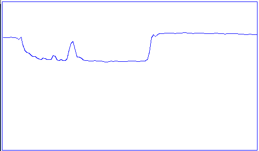
Transmitter E93.9 has average value 43.0 counts, gain 0.6 dB lower than a week ago. It does not produce jumps in average signal value. We put the three transmitter back in the hot water and watch their signals. E90.14 is stable at 50 kcount. E93.9 stable at 43 kcount. E93.2 spending most of its time at 43 kcounts, but jumping up to 51 kcounts frequently. Six hours later, average values are stable, with apparent battery voltage 2.87 and 2.81 V for No2 and 9 respectively, and noise around 10 μV.
Transmitter E90.14 is still running but battery voltage appears to be 1.98 V and reception is poor. We dissect E90.14. Battery voltage is 2.76 V. Active current 78.5 μA. Center frequency 912 MHz. Average value 56 kcounts. By now, active current has dropped to 74.1 μA. We measure VA on C5 to be 2.0 V. We are supplying 2.7 V from a power supply. We measure VA on R4 and see variation from 2.0-2.7 V. The average value of the signal varies in sympathy. We are pushing on R4 and C5 when the average value suddenly stabilizes at 43.7 kcounts, noise is 10 μV. Reception is 100%. Current is now 91 μA. We measure VA = VD = 2.7 V and 1V8 = VC = 1.8 V on C4 and C6 respectively. We turn our supply voltage down to 1.85 V and quiescent current drops to 75 μA while average value rises to 61 kcounts. We solder the battery back to the circuit board. We have replaced nothing on the board. It now functions perfectly.
There are two ways for VA to drop 0.7 V below VB. One is for the VA current to be 700 μA so the drop across R4 will be 0.7 V. Another is for one of the two U1 mosfet switches to be partially off. We drive U1-5 with a logic chip. But U1-2 is held to 0V with 10 MΩ. We suggest that condensation is compromising the isolation of gate U1-2, causing a 10-MΩ resistance between the gate and nearby source U1-1.
We remove E93.2 from the oven and drop into cold water, then place in faraday enclosure. Average value is 43 kcounts. Ater a few minutes, we start to see sudden jumps in average value, settling to a baseline of 48 kcounts. Jumps are 10 kcounts in amplitude. We record to disk and obtain this overview of 1000 s from M1448397508.ndf, during which the average value settles back to a stable value of 43.8 kcounts (VA = 2.7 V). The behavior of E89.2 is consistent with that of E90.14 and E93.2: jumps in average value without increased current drain. We will call this the "resistive switch" problem.
We have B91.1, 8, 10, and 12 encapsulated with vacuum dip, two drips off the transmitter during 60 s, then 30 s invert to let epoxy flow back, rotate, another coat of epoxy on the bottom side of the board (which we call the "top-coat" for some reason), and five coats of silicone. Dimensions 8.3 mm × 13.8 mm × 14.5 mm (1.7 ml block volume). Also, B91.2, 3, 6, 9 one drip off transmitter during 30 s, then 30 s invert, five coats silicone, 9.0 mm × 14.4 mm × 15.4 mm (2.0 ml block volume). These have the support wire for the rotator clipped off but still visible through the silicone. We measure hand-made B76.10 as 8.3 mm × 13.7 mm × 14.3 mm (1.6 ml block volume). In each case, we take the average of multiple measurements of each dimension around the edges. The B91 circuits are all A3028AV3. We measure frequency response, see here. We turn all the B91 devices on and put them in the oven for 24hr/60°C/D/ON burn-in.
[25-NOV-15] Batch B91 has survived burn-in, we get perfect reception, battery voltages 2.68-2.78 V, and noise around 10 μV. We put them all in the oven to poach.
Transmitter E93.9 is running fine with VA = 2.7 V, but we get no signal from E93.2. We put it in the oven to dry out. Two hours later we still cannot turn on the device. Battery voltage 2.57 V. Disconnect battery. Connect external 2.6 V. Current is 150 mA. We turn off and clean up solder joints. Reconnect power. Active current 90 μA. Now getting reception. Re-connect battery. Reception 100% in faraday enclosure. Gain versus frequency is within 0.1 dB of our measurement pre-poach on 17-NOV-15. Battery voltage 2.61 V, according to average signal value of 46.2 kcount, VA = 2.55 V. Noise is 50 μV. Clear epoxy from around C2, C5, and R4. Transmission stops. Battery voltage 2.7 V. VD = VA = 0.3±0.1 V. VB at U1-1 is 2.7 V. Turn off with magnet and VD = VA = 0.0 V. U1-2 is at 2.7 V. U1-6 = U1-4 = U1-3 = 0.3 V. We connect U1-2 to 0V with ammeter and measure 3 mA. Resistance between U1-2 and VB is 0.0 Ω. We remove U1 with the help of aqueous flux. Don't see corrosion underneath. Wash and dry. Resistance U1-2 to VB is 15 MΩ. We compare the underside of the U1 we removed to a fresh U1. We see no difference. On the footprint of U1 we see epoxy film across the lower of two vias, but not across the upper via, which connects U1-2 to an inner layer. The upper via is not filled with epoxy, and the surface between the via and U1-1 is uncovered.
If we cool a transmitter that is saturated with water vapor, and the U1-2 via is not sealed, condensation in this region will connect U1-1 to U1-2, turning off the mosfet, which will lead to VA dropping. In heat, we speculate that this water will cause corrosion and create a short circuit that will turn off the transmitter. This is our best guess as to the source of the resistive switch problem.
[30-NOV-15] Transmitter E93.9 still going strong, picks up mains hum, and battery voltage 2.7 V. Of the eight transmitters of Batch B91, all are running well and picking up mains hum with battery voltage around 2.7 V, except B91.3, which won't turn on. We put it in the oven to dry out, return all the rest to water to continue poach.
[01-DEC-15] Transmitter B91.3 still does not turn on. We photograph the cut-off wire, which is rusted, as it is in the other three with the cut-off wire covered only with silicone. We see thin cover on peripheral capacitors, as shown below.

We dissect B91.3. Silicone well-adhered to epoxy. We measure the thickness of the five coats of silicone in various places as we remove it. Estimate the average thickness to be 0.6 mm, consistent with the MED10-6607 data sheet, which specifies 5 mils per coat. We try to solder to the end of the cut-off rotation support lead, after removing silicone, but the lead end refuses to solder until we apply acid flux. Battery voltage 1.2 V. Detach battery and connect 2.6 V. Inactive current 1.7 μA. Active current 45 mA. We remove C5, C4, C6, and C3. Active current remains 45 mA. If we have a short circuit created by corrosion between two power supply pins, we will get such a drain. If the short occurs between U1-1 and U1-2 we get the resistive switch problem. We are diagnosing this as an "Unidentified Drain".
For B91.1, 2, 6, 8, 9, and 12 battery voltage is 2.55-2.60 V. Noise is 10 μV except in B91.12, where we see 20 μV. The noise in B91.12 turns out to be 22-Hz switching noise, fundamental 10 μV, 2nd harmonic 8 μV, 3rd 4 μV, 4th 4 μV.
Transmitter E93.9 has been running fine, but after cooling down, shows steps in its average value, as in the resistive switch problem. We put it back in the oven to poach. After a few hours we take it out again and VA is stable at 2.6 V. Gain versus frequency within 0.1 db of measurement on 17-NOV-15.
[04-DEC-15] We have batch C94.1-8, 0.3-80 Hz using Y in the A3028AV5 assembly. The Y channel amplifier in this assembly is set to 0.3-80 Hz. Gain versus frequency shown here are all within ±0.5 dB. Switching noise 4 μV or less. Battery voltage 2.52-2.65 V. Reception 100%. Total noise less 6-8 μV.
Of the transmitters poaching, E93.9, B91.6, and B91.10 no longer transmit. The remainder, B91.1, 2, 8, 9, and 12 have battery voltages 2.48-2.64 V. Reception is perfect and noise is less than 10 μV.
After an hour sitting in air on our bench, B91.10 transmits. We get poor reception in faraday enclosure, VA = 1.9 V. Dissect. Silicone is so well adhered to epoxy that we must shave it off. Battery voltage 2.74 V. Inactive current 1.6 μA, active 62 μA no reception. Apply heat gun to bottom side, active current 72 μA some reception. Heat U1 up with solder blob for 20 s. Wash and dry. Active current 90 μA for thirty second, reception perfect. VA = 2.7 V. Current drops down to 60 μV and we lose reception. Replace R2 with 0Ω. Active current 100 μA, VA matches our applied VB. After thirty seconds, VM drops to 1.0 V, current jumps to 3.7 mA, and VB has dropped to 1.0 V because of he impedance of our ammeter. We see U1-2 at 0V. We switch to milliammeter and current jumps up to tens of milliamps then drops to 100 μA. After thirty seconds, jumps up to 4 mA and reception continues. We turn off and on again. Current is 90 μA and remains so for twenty minutes. Remove U1. Note that both vias under the chip are filled with black epoxy.
We dissect E93.9. Silicone comes off easily with the black varnish. Battery voltage 2.5 V. Current consumption jumps up to 3 mA briefly. When 80 μA get good reception. After one minute, current settles to 80 μA. We see no aberrations for twenty minutes.
We dissect B91.6. Silicone is well-adhered to epoxy. Battery voltage before disconnecting is 0.5 V, after disconnecting 1.0 V. Connect 2.6 V. Inactive current 25 mA. Remove glue from around C2. Inactive current 21 mA. Remove C2. Inactive current 21 mA, erratic. We have VB = 2.7 V, VA = 0.5 V, VD = 0.5 V, VM = 2.7 V. Heat up epoxy around U1 with intent to measure voltages on it. Current drops to 10 μA, VM = 2.7 V, VD = 0.5 V. U1-5 = U1-4 = VM. We see U2-2 switching with magnet. But the circuit does not switch on. We see U3 is displaced on its footprint.
The failure of B91.10 is consistent with the resistive switch problem. The Failure of E93.9 and E91.6 are appear to be due to a short between U1-5 and U1-4, which results in VD being turned off, and current being drained through U3. We observed a short between U1-1 and U1-2 before, so U1-5 and U1-4 could also be shorted by corrosion. But we were unable to measure this short directly today. We classify this problem as a "corrosion short".
[07-DEC-15] Of the 5 transmitters poaching, B91.1, 2, 9, and 12 are running well, with battery voltages 2.58-2.69 V. But B91.8 does not transmit. (See 08-DEC-15 below for possible explanation: we had B91.8 and B91.9 mixed up.) We leave it out on our work bench to dry and put the others back. When we return to our bench, B91.8 is running. Battery voltage 2.61 V. Gain versus frequency has changed: the bump at 130 Hz is gone, see here. Put back in the oven to poach.
[08-DEC-15] We have batch C94.1-8 after four days soaking in water. All detect heartbeat. Battery voltages 2.57-2.70. Noise less than 12 μV. Reception perfect. This is the first batch of circuits made with the A3028AV5 circuit. We put C94.3 and 4 in the oven to poach, and ship the rest to ION.
Of B91.1, 2, 8, and 12 are running well. Battery voltages 2.4, 2.62, 2.62, 2.50 V respectively. Noise less than 12 μV. Reception perfect. We measure gain versus frequency and plot B91.1, B91.2, B91.8, B91.12. B91.1 and B91.8 show gain 3 dB too low, while the others are within 0.1 dB of their original gain. B91.9 does not run at all. We suspect that B91.9 was not running yesterday morning either, but in our haste, and with an Octal Data Receiver with no channel number labels, we mixed up B91.8 and B91.9. We will assume this mix-up took place. We now dissect B91.9. Battery voltage 1.6 V. Solder leads to VB and 0V. Transmitter starts working on its own battery for thirty seconds, turns off. Apply 2.6V. Active current 90 μA. Inactive 1.6 μA. Picks up mains hum, reception perfect. Battery, now disconnected, has recovered to 2.3 V. We connect a fresh battery and measure frequency response B91.9. We are going to call this "Unidentified Drain".
[11-DEC-15] B91.1, 2, and 8 have all stopped. B91.12 is running well, VA = 2.53 V, reception perfect, noise 19 μV. C94.3 and 4 are running well, VA = 2.71 and 2.67 V, reception perfect, noise 7 μV.
We dissect B91.2. Battery voltage 0.0 V. Disconnect battery, 1.0 V. Connect external 2.6 V. Transmitter switches on and off. Inactive current consumption climbs from 20 μA to 4 mA in two minutes, and is still climbing. Transmitter still turns on and off, now with active current 5.07 mA and inactive 5.00 mA. Remove C2. Inactive consumption 1.8 μA, active 66 μA. Reception intermittent. Resistance between C2 terminals is 36 Ω. Clean with solder and alcohol, still 36 Ω. Replace C2 with fresh part. Active current 83 μA. Reception perfect. Connect to a battery. With voltmeter, VB = 3.2 V, with X, VA = 3.2 V. Measure frequency response follows same shape as earlier measurements, but is lower because of elevated battery voltage. Classify as "corroded capacitor".
We dissect B91.8. Battery voltage 1.3 V. Disconnect battery, 2.1 V. Connect external 2.6 V. Inactive 1.7 μA, active 280 μA and climbing. Robust reception. Average X 31k. Active current now 800 μA, average X 25k. Remove C6. Active current 90 μA. Average X 45k. Resistance of removed C6 is ∞. Measure gain, it is farther off than it was a few days ago, B91.8. Classify as "corroded capacitor".
We dissect B91.1. Battery voltage 1.8 V. Disconnect battery, 2.8 V. Connect external 2.6 V. Inactive 1.8 μA. Active 88 μA. Average X 45k. Gain has dropped farther, see B91.1. If we drive X with a 50-Ω source, gain versus frequency is perfect. We classify this failure as "unidentified drain".
We have batch E95, consisting of E94.1-95.7, made from AV5 circuits. Gain versus frequency as shown in E95. All look good except E95.3, with gain far too low at 100 Hz, and E94.12, which has no bump in gain at 120 Hz. Battery voltages 2.54-2.77, reception perfect, noise less than 12 μV. Switching noise less than 4 μV. We fail E94.12 and E95.3 for frequency response and put them in the oven to poach. Ten of the remainder ship today.
We are ordering another 50 AV5 circuits with lead-free solder, no-clean process, and paste printer. These will be AV5LF for lead-free.
[15-DEC-15] We have five devices poaching. We remove them from hot water for approximately three minutes in dry air. C94.3 and C94.4 have robust reception, VA = 2.78 and 2.76 V respectively. B91.12 robust reception, VA = 2.63 V. E95.3 and E95.12 robust reception, VA = 3.05 and 2.78 V respectively. Noise below 12 μV.
[17-DEC-15] Of five devices poaching, C94.3 and C94.4 have robust reception, VA = 2.78 and 2.76 V respectively, which we note is identical to the values we obtained two days ago. B91.12 has stopped transmitting after running continuously for 23 days, 22 of which were at 60°C in water. E94.12 and E95.3 have robust reception, VA = 2.82 and 2.85 respectively, noise below 7 μV.
[18-DEC-15] E94.12 and E95.3 have robust reception, VA = 2.80 and 2.85 V respectively, noise below 7 μV. C94.3 and C94.4 have robust reception, VA = 2.77 and 2.75 V respectively, noise below 7 μV.
[21-DEC-15] C94.3 and C94.4 have robust reception, VA = 2.88 and 2.73 respectively. Noise less than 9 μV. E95.3 and E94.12 have robust reception, VA = 2.84 ad 2.76 V respectively, noise less than 8 μV.
[22-DEC-15] C94.3 reception robust, VA = 2.81 V, noise 6.6 μV. C94.4 reception robust, VA = 2.73 V, noise 9.0 μV. E95.3 reception robust, VA = 2.85 V, noise 6.5 μV. E94.12 not transmitting. We dissect. The silicone comes off the enamel-painted surface easily in one piece, with some of the enamel coming with it. There are three cavities in the epoxy top-coat. Covering over some of the capacitor corners is thin. Battery voltage 2.9 V. Remove C2 and C5. Battery voltage appears on VB. Connect external 2.6 V. Current consumption 0.2 μA. U1-2 varies 2.5±0.4 V when we apply 10-MΩ probe. Resistance U1-2 to 0V is 11 MΩ. Resistance U1-2 to VB is 0.5 MΩ. This is the resistive switch problem. We replace R2 with 100 kΩ. We replace C1 and C5. We wash and blow dry. Inactive current consumption is 26 μA and resistance from U1-2 to VB is now 2 kΩ. We dry in the oven. No change. We replace R2 with 0 Ω. Now inactive current consumption is 1.6 μA, active 60 mA. We have VA = 1.8 V. VM = 2.2±0.1 V. This is a corrosion short problem. We remove U1, R2, C2, C5, clean, and dry. Resistance from U1-2 to VB is ∞ and from U1-5 to VM is 1.7 MΩ.
U1 is directly below the epoxy cavity. We examine batch E97 and find that 6 of 14 have bubbles in the top-coat (the coat of epoxy on the bottom side of the board, over U1, C2, C5). In three cases, there is a bubble over U1, but not in the other three cases. We note that we saw the resistive switch and corrosion short problems in our rotator-encapsulated batch B91, which had no bubbles nor enamel, and silicone was well-adhered to entire surface. These AV5 circuits are made with a water-free process, made with paste printer and leaded solder. Our only hypothesis to explain the problem under U1 is that we are not washing our flux off sufficiently after loading the battery. We started double-washing the circuit after battery loading with batch C95 a couple of weeks ago.
We have batch C95, consisting of A3028C-AA numbers C95.8-C96.5. This is the first batch we double-washed after battery loading. Frequency response is C95_G_vs_F, all within ±0.8 dB at the bump, and ±0.2 dB elsewhere. Reception is robust, battery voltages 2.51-2.60 V, noise less than 12 μV, switching noise less than 4 μV. We take C96.4 and C96.5 for aging tests. We turn them on and put them in the oven to poach.
[23-DEC-15] C94.3 reception robust, VA = 2.80 V, noise 5.3 μV. C94.4 reception robust, VA = 2.71 V, noise 9.3 μV. C96.4 reception robust, VA = 2.81 V, noise 4.9 μV. C96.5 reception robust, VA = 2.77 V, noise 5.8 μV. E95.3 not transmitting.
[24-DEC-15] C94.3 reception is 70%, VA = 2.79 V, noise 5.0 μV. We remove from hot water and allow to cool down. Reception is 100%. Frequency response C94_3_G_vs_F is within 0.2 dB of 20 days ago. C94.4 reception robust, VA = 2.61 V, noise 7.0 μV. C96.4 reception robust, VA = 2.82 V, noise 4.7 μV. C96.5 reception robust, VA = 2.78 V, noise 6.0 μV. E95.3 has been sitting on our bench drying out. Still does not transmit. We dissect. Silicone comes easily off the enamel. Battery voltage 3.0 V. Connect external 2.6 V. Inactive current 0.5 μA. Cannot activate. Clear epoxy around R2. Current 0.5 μA. Measure voltage on U1-2 where is appears on R2, get 2.6 V. Measure resistance U1-2 to VB, get 3.8 kΩ. We clear epoxy from around U2. Resistance U1-2 to VB now 20 MΩ. Connect power, inactive current 1.6 μA, active 85 μA. Measure frequency response C95_3_G_vs_F and note that original problem with response has disappeared. We obtain the following photograph of U1, which shows a dendrite growing from U1-1 towards U1-2.

The dendrite remains shiny regardless of the angle of our light. We remove it with tweezers and photograph it alone. We bend it with our tweezers. We unbend it. It's tiny, but we are certain it is metallic. We note that E94.3 is made with the lead-free AV5 circuit. The dendrite did not form beneath U1, but between its pads. For this to occur, something must have occupied space between the pads to stop epoxy from insulating them from one another. Subsequently, whatever space filler was present took part in migration of Sn or Pb between the two terminals with 2.7 V driving the reaction.
These boards are made with lead-free solder, a solder paste printer, and covalent chemical wash. The U1 package is lead-free, but that's because its copper pins are coated with tin. The circuit boards themselves are gold-plated copper. There should be no silver around U1. The dendrite is made of lead or tin or both. In Choi et al. the authors measure the electromigration activation energy for SnPb solder, and obtain a value of 0.77 eV. The activation energy for silver dendrite formation was measured by Hornung to be 1.1 eV. In this report, they claim silver is much more likely to migrate than tin or lead. But let us suppose the activation energy for SnPb migration is 0.77 eV. In that case, our acceleration factor for 60°C (333 K) compared to rodent body-temperature 37°C (310 K) is exp(0.77/310k −0.77/333k) = 71. For an activation energy of 1.1 eV the factor is 16. Because this resistive switch failure is PbSn, it's likely that onset at 11 days at 60°C implies onset at 780 days at 37°C.
[28-DEC-15] We have batch E96.6-97.3, which we call E96, after 24hr/60°C/D/ON and 72hr/20°C/W/OFF. Reception is perfect from all devices. Gain versus frequency within 1 dB of nominal, see E96_G_vs_F. Switching noise less than 6 μV. VS = 2.57-2.64 V.
We take C94.3 out of 60°C water and let it cool down for one minute. Reception is 100%. VA = 2.54 V. Frequency response C94_3_G_vs_F looks good. We place in 45°C water, RF center frequency 909 MHz. Transmitter C94.4 we remove from 60°C water, frequency response C94_4_G_vs_F. Transmitter C96.4 reception perfect, VA = 2.81 V, noise 5.3 μV. Transmitter C96.5 reception perfect, VA = 2.77 V, noise 5.76 μV. We start testing of transmitters E97.2 and E97.3, both AV5 circuits, both double-washed.
[30-DEC-15] We check 6 transmitters that have been poaching at 60°C. Transmitter C94.3 reception perfect, VA = 2.56 V, noise 8.8 μV. Transmitter C94.4 reception perfect, VA = 2.45 V, noise 8.28 μV. Transmitter E97.2 reception robust, VA = 2.79 V, noise 6.7 μV. Transmitter E97.3 reception robust, VA = 2.81 V, noise 6.6 μV. Transmitter C96.4 reception robust, VA = 2.82 V, noise 4.5 μV. Transmitter C96.5 reception perfect, VA = 2.79 V, noise 5.8 μV.
We have batch E97.4-98.2, AV5 circuits. Gain versus frequency E97_G_vs_F. Noise <10 μV, switching noise less than 4 μV, all 19-21 Hz.
[02-JAN-16] E94.3 no longer transmitting, even after cool-down. Dissect. Battery voltage 0.6 V. With external 2.6-V supply, inactive current 1.6 μA, active 11 mA, transmitter turns on, perfect reception, VA = 2.5 V. Replace C4, no change. Reduce external supply to 2.2 V, active current 9 mA. Replace C3. Current 9 mA. No other capacitor failure can give these symptoms. Classify as Unidentified Drain.
E94.4 transmits briefly then stops. Dissect. Battery voltage 1.7 V. Apply external 2.6 V. Inactive current 1.7 μA, active 50.0 μA. Reception perfect. VA = 2.5 V. At 50 μA, this transmitter should have run for 40 days. But here we see it expiring after 25 days. Classify as Unidentified Drain. This is our longest-lived transmitter equipped with a BR1225 battery so far.
E97.2, E97.3, C96.4, C96.5 running well. Reception robust. Battery voltage and noise are E97.2 2.80 V and 6.5 μV, E97.3 2.83 V and 6.9 μV, C96.4 2.75 V and 5.9 μV, C96.5 2.77 V and 5.9 μV. Put them back in the oven.
[05-JAN-16] E97.2, E97.3, C96.4, C96.5 running well. Reception robust. Battery voltage and noise are E97.2 2.82 V and 6.3 μV, E97.3 2.84 V and 6.5 μV, C96.4 2.81 V and 4.8 μV, C96.5 2.77 V and 4.9 μV. Put them back in the oven.
[06-JAN-16] All four poaching devices are transmitting, but we perform no other tests.
[08-JAN-16] C96.4 no longer transmitting. E97.2, E97.3, and C96.5 perfect reception. E97.2 2.78 V, 8.6 μV. E97.3 2.81 V, 8.9 μV. C96.5 2.73 V, 9.1 μV. We dissect C96.4. After removing silicone, we break through a thin layer of epoxy and enamel, to find this cavity with metal visible at the bottom. The cavity is above C10, C11, U5-4.

Battery voltage 0.1 V. Apply external 2.6 V. Inactive current 1.7 μA, active 2.4 mA. We record full-range mains hum. Remove R4, active 52 μA. The X signal is stuck at 0. Because R4 supplies VA and is 1 kΩ, 2.4 mA would be consistent with VA = 0.2 V, which precludes detection of mains hum. When we remove R4, current returns to normal, and U7 is disabled. Measure R4 as 1.000 kΩ. Replace C2, C5, and R4. Active current 2.5 mA. VA = 0.2 V. Clean and dry. VA = 0.2 V, 1V8 = 1.8 V. Clear epoxy from around these parts. Transmitter now turns on, records mains hum, current 55 μA, VA = 2.6 V. It looks like a short developed beneath the cavity. We removed the short when we cleared the epoxy. The one confounding observation is mains hum when we were apparently consuming 2.4 mA, but our 2.4 mA and mains hum observations were consecutive, not simultaneous. We invent a new classification for this problem: Cavity Drain.
We take B84.9 and B86.1 off the shelf and measure their frequency response. We plan to ship these to Newcastle as additional samples.
[11-JAN-16] Transmitter E97.2 perfect reception, VA = 2.83 V, noise 6.6 μV. E97.3 robust reception, VA = 2.85 V, noise 6.9 μV. C96.5 perfect reception, VA = 2.75 V, noise 5.3 μV.
[12-JAN-16] Transmitter E97.2 robust reception, VA = 2.81 V, noise 7.3 μV. E97.3 perfect reception, VA = 2.84 V, noise 6.9 μV. C96.5 robust reception, VA = 2.72 V, noise 8.6 μV.
We have batch E98.3-E99.4, a batch of sixteen A3028E. All turn on and off except E98.14. Dissect. Battery 1.4 V. Apply 2.6 V. Inactive current 1.6 μA, active 84 μA. Reception perfect. Picks up mains hum. The remaining 15 have perfect reception, switching noise less than 4 μV. All have gain versus frequency within range ±0.4 dB, E98_G_vs_F. We ship 14 transmitters and keep E98.13, which we put in the oven to poach.
In making batch E99.5-100.2 we notice after vacuum-cycling the top coat that there are bubbles 0.5 mm or so in diameter pressing up against the surface tension of the epoxy. We burst these with a metal point, and find in many cases that the bubble underneath is of diameter far larger than the visible circle on the epoxy, so that when we pop the bubble we see 1 mm down into the epoxy, sometimes glimpsing the components. In the past three months, we have been using a new vacuum chamber that provides a better seal and lower vacuum. After bursting the bubbles, more appear, and we burst these too. After the fourth run through the batch, there are no more large bubbles left.
[14-JAN-16] For E97.2, E97.3, C96.5, and E98.13 we get the following from a one-second interval. No2: 512 samples, VA = 2.81 V, noise = 6.7 μV; No3: 512 samples, VA = 2.84 V, noise = 7.0 μV; No5: 256 samples, VA = 2.71 V, noise = 8.8 μV; No13: 510 samples, VA = 2.80 V, noise = 7.7 μV.
We have batch C99.5-100.2, 12 of A3028C-AA. These are the first transmitters we have made with the BR1225 battery with corners cut off, as shown below.

We stuff them all into a 50-ml beaker and cover them with water, antennas and all. The water comes up to the 40-ml mark. We remove the transmitters. The water drops to 24 ml. The volume of each device is 1.3 ml. All of them turn on and off and give robust reception. We put them in the oven to burn in.
[15-JAN-16] Batch C99.5-100.2 have survived burn-in. Battery voltages 2.67-2.75 V. Noise less than 11 μV. Reception robust. We turn them all off and put them in room temperature water. For E97.2, E97.3, C96.5, and E98.13 we get the following from a one-second interval: No2: 512 samples, VA = 2.82 V, noise = 6.6 μV; No3: 512 samples, VA = 2.85 V, noise = 7.2 μV; No5: 256 samples, VA = 2.70 V, noise = 15.4 μV; No13: 512 samples, VA = 2.81 V, noise = 7.8 μV;.
[16-JAN-16] Batch C99.5-100.2 have soaked for 24 hours. We measure gain versus frequency, C99_G_vs_F. C99.6 gain is higher than usual and its battery voltage is lower, which are correlated symptoms. We apply 5-mV sweep and scale the response to account for lower battery life and amplitude, and we get good agreement with the other transmitters. Simultaneous reception from all twelve gives us: No1: 247 samples, VA = 2.59 V, noise = 9.5 μV; No2: 256 samples, VA = 2.59 V, noise = 7.4 μV; No5: 251 samples, VA = 2.58 V, noise = 6.2 μV; No6: 255 samples, VA = 2.48 V, noise = 6.5 μV; No7: 256 samples, VA = 2.54 V, noise = 7.5 μV; No8: 256 samples, VA = 2.55 V, noise = 6.4 μV; No9: 256 samples, VA = 2.55 V, noise = 7.1 μV; No10: 256 samples, VA = 2.51 V, noise = 8.4 μV; No11: 255 samples, VA = 2.51 V, noise = 9.4 μV; No12: 253 samples, VA = 2.51 V, noise = 8.9 μV; No13: 257 samples, VA = 2.55 V, noise = 7.4 μV; No14: 249 samples, VA = 2.56 V, noise = 8.5 μV.
For E97.2, E97.3, C96.5, and E98.13 we get the following in one second. No2: 509 samples, VA = 2.83 V, noise = 6.4 μV; No3: 135 samples, VA = 2.86 V, noise = 6.9 μV; No5: 207 samples, VA = 2.30 V, noise = 11.7 μV; No13: 511 samples, VA = 2.84 V, noise = 7.6 μV. C96.5's battery appears to be failing. Given low battery voltage, gain versus frequency still looks perfect, and reception is perfect.
[20-JAN-16] E97.2, E97.3, and C98.13 still running. C96.5 stopped.
[21-JAN-16] E97.2, E97.3, and E98.13 still running.
[26-JAN-16] E97.2, E97.3 still running. No2: 508 samples, VA = 2.53 V, noise = 7.1 μV; No3: 501 samples, VA = 2.85 V, noise = 7.0 μV. Frequency response of E97.3 looks good. But by the time we come to measure the response of E97.2, we have VA = 1.9 V, suggesting a resistive switch problem, which tends to manifest itself when the device cools down. E98.13 has stopped. Dissect. Note that corner of C2 at edge of epoxy appears to be exposed after removal of silicone and enamel. Battery voltage 0.0 V. Disconnect battery, voltage is 1.9 V and rising, 2.3 V after 50 s. 2.7 V after 10 minutes. Connect external 2.6 V and see 5 mA, increasing to 6 mA. Reception 100%. Current 15 mA after 2 minutes. Turn off and current remains 13 mA. Remove epoxy from C2 and C5. Active current 5 mA. Remove C2. Inactive current 2.7 μA, active current 3 mA. Examining C2, we see a flake of ceramic coming off the top side. It falls off. The capacitor is thinner. Resistance is 0.8 Ω. The fact that the battery recovers so quickly from being drained suggests that the failure happened within the past 24 hrs. Remove C5. Resistance is 50 Ω, capacitance 2 nF. Replace C5. Active current 82 μA. Reconnect battery and transmitter runs well at first, but battery voltage drops to 2.2 V after a few minutes, and we are unable to measure frequency response with 10-mV sinusoid. We attach fresh battery and measure gain versus frequency. Gain is within 2 dB of nominal for the 3.0 V battery. Diagnosis: corroded capacitor failure.
Dissect C96.5. Battery voltage 0.1 V. Disconnect battery, its voltage is 0.2 V. Connect external 2.6 V. Inactive 2.6 μA. Active 53 μA. This transmitter ran for a total of 30 days (1 day burn-in, 29-day poach). Charge consumption should have been 36 mA-hr. Battery capacity is 48 mA-hr. Diagnosis is Unidentified Drain.
We have a new protected-input layout, A302801F. We reduce the length of the board from 565 mil to 550 mil. The width remains 500 mil. The height and width of the A302801D layout, which we have been using for the past several hundred transmitters, are both 500 mil. This new board will be 1.3 mm longer than the one we have been using. The BR1225 mounting holes remain as they were. We remove the holes for BR2330 battery. The 0V tab now has a 50-mil pad on the bottom side only, anchored with a 20-mil via. The VB tab solders to the rim of the BR1225 VB hole. We expand the rim where the BR2330 tab will fold over the circuit board. We move C2, C5, and C4 so they are at least 50 mil from the board edge. Previously C2, C4, and C5 were 25 mil from the edge. All 10-μF capacitors are now 50 mil or farther from the edge. These parts are tall, and had been pressing up against the meniscus of our epoxy. We make octagonal pads for A, C, X, and Y on the top side of the board only, where we solder the leads. Each pad is held in place by a 20-mil via. The identity of each pad is marked on the bottom-side silk screen. We add an isolated pad at the center of the top edge on the top side of the board for a holder wire to be attached. The pad is anchored with a 20-mil via. We reduce the 30-mil vias to 20 mil because we do not plan to use holes for evacuating air. We will be forcing epoxy into the circuit while the circuit is in vacuum. Our A302801D mouse transmitters now have volume 1.3 ml, with the trimmed battery, rotator encapsulation, and top-coat of epoxy. The A302801F will be 1.3 mm longer, producing a ledge beneath the battery 12.5 mm wide and 1.3 mm deep. When covered with 2 mm of epoxy top and bottom, the increase in volume will be only 0.01 ml. We have moved the capacitors in from the edges, so we should now be able to eliminate the top coat, which will save us a 0.5 mm depth on a 12.5 mm square, saving us 0.08 ml.
[28-JAN-16] Yesterday, E97.2 and E97.3 were going strong. We left them out of the oven. Today E97.3 has stopped, but E97.2 is still going strong.
[29-JAN-16] E97.2 still running: 511 samples, VA = 2.40 V, noise = 8.2 μV. We dissect E97.3. VB = 0.9 V. Disconnect, VB = 2.5 V after a few minuts. Connect external 2.6 V. Current is at first 2 mA with the microammeter, switch to millammeter and current drops to 0.08 mA. Switch off. Inactive current 1.6 μA. Switch on, active current 80 μA. Reception perfect, picks up mains hum. This device failed after cool-down to room temperature. The battery recovers to 2.55 V. After 30 days at 80 μA, the battery voltage should still be 2.7 V (58 mA-hr used of 255 mA-hr capacity). Diagnosis is Unidentified Drain.
We assemble our first A3028H, a two-channel 256 SPS, 0-80 Hz EEG/EMG monitor. We replace C9, C10, and C11 on an A3028AV5LF with 2.0 nF. We program one and measure frequency response, see here.
[01-FEB-16] E97.2 still running: 512 samples, VA = 2.29 V, noise = 18.7 μV.
[02-FEB-16] We have batch E100.13-14. Gain versus frequency is E100_G_vs_F. Switching noise less than 5 μV, 20-22 Hz. From a one-second interval, all transmitters together in water we get robust reception and noise less than 10 μV. E97.2 still running: 512 samples, VA = 2.08 V, noise = 9.6 μV;. We put E100.13 and E100.14 in to poach.
[03-FEB-16] E100.13 and E100.14 running. For 1-s interval No13: 512 samples, VA = 2.86 V, noise = 6.2 μV; No14: 512 samples, VA = 2.85 V, noise = 6.1 μV. E97.2 has stopped. We cut open the silicone and it starts running again. For 1-s interval on bench-top: 512 samples, VA = 1.93 V, noise = 15.5 μV. Turns off again. VB = 1.8 V. Disconnect battery, VB recovers to 2.0 V in one minute. Connect external 2.60 V. Inactive current 2.1 μA. Active 84 μA. For 1-s interval 512 samples, VA = 3.05 V, noise = 12.8 μV. No mains hum pick-up. Meanwhile, battery has recovered to 2.35 V. Diagnosis is Unidentified Drain.
[04-FEB-16] For E100.13 and E100.14 we get in 1-s interval in faraday enclosure. No13: 481 samples, VA = 2.84 V, noise = 8.6 μV; No14: 483 samples, VA = 2.82 V, noise = 6.8 μV. We measure their RF spectrum and find its peak at 909 MHz and range 900-918 MHz.
[06-FEB-16] We have a wire stripper capable of displacing a 1-mm section of teflon insulation around a 125-μm Pt-Ir wire. We prepare a new version of the H-Electrode that we first developed last year. We will prepare twelve of these for ION-UCL.

Construction of this version is simpler because we have only two wires to join.
E100.13 and E100.14 running well. No13: 504 samples, VA = 2.86 V, noise = 8.3 μV; No14: 375 samples, VA = 2.85 V, noise = 6.4 μV.
[08-FEB-16] E100.13 and E100.14 running well. No13: 512 samples, VA = 2.86 V, noise = 6.6 μV; No14: 512 samples, VA = 2.85 V, noise = 6.4 μV. Batch B102.4-13 has been soaking in water for 3 days. We measure frequency response with a 5-mV peak to peak waveform and get B102_5mV. In water, VA = 2.51-2.55 V, noise less than 12 μV, reception robust.
[09-FEB-16] E100.13 and E100.14 running well. No13: 512 samples, VA = 2.84 V, noise = 6.5 μV; No14: 512 samples, VA = 2.82 V, noise = 7.0 μV. We have batch H103.1-9 (odd numbers only), six A3028H-AAA dual-channel 0.3-80 Hz transmitters. They have survived 72hr/20C/W/OFF and 6hr/60C/D/ON. Frequency response of all channels recorded in H103_5mV, all good. We have batch C101.1-102.3, seventeen A3028C-AA single-channel 0.3-80 Hz transmitters. They have survived 24hr/60C/ON/D, 72hr/20C/OFF/W, 6hr/60C/ON/D. Frequency response of all devices recorde in C101_5mV_A and C101_5mV_B, all good except C101.11, which shows low gain. During manufacture, we observed cavities beneath the epoxy in devices C101.6, C101.11, and C101.13. We keep as spares H103.1 and B101.13. We put C101.11 (low gain and epoxy cavity), C101.13 (epoxy cavity), and B102.12 in the oven to poach.
[10-FEB-16] C101.11, C101.13, B102.12 all running: No11: 255 samples, VA = 2.76 V, noise = 4.1 μV; No12: 512 samples, VA = 2.74 V, noise = 7.8 μV; No13: 250 samples, VA = 2.76 V, noise = 5.4 μV. E100.13 and E100.14 running well: No13: 512 samples, VA = 2.87 V, noise = 12.9 μV; No14: 510 samples, VA = 2.85 V, noise = 9.7 μV.
[11-FEB-16] C101.11, C101.13, B102.12 running well. Reception 100%. VA = 2.70-2.74 V, noise less than 11 μV. E100.13 and E100.14 running well. Reception 100%. VA = 2.84-2.86 V, noise less than 7 μV.
[18-FEB-16] E100.13 and E100.14 running well. Reception 100%, VA = 2.84-2.86 V, noise less than 7 μV. C101.11 and C101.13 running well. Reception 100%, VA = 2.70-2.70 V, noise less than 7 μV. B102.12 shows 80% reception until we remove it from the hot water, then we get 100% and VA = 2.31 V. We measure gain versus frequency, and it is uniformly 0.8 dB higher than on 08-FEB-16.
[19-FEB-16] E100.13 and E100.14 running well. Reception 100%, VA = 2.86-2.88 V, noise less than 7 μV. C101.11 and C101.13 running well. Reception 100%, VA = 2.76-2.77 V, noise less than 6 μV. B102.12 100% reception, noise 14 μV, VA = 2.26 V. If VA = VB, then yesterday VB was 2.3 V, and today should be drained below 2.0 V by 80-μA consumption of the A3028B. The fact that VA dropped only 0.05 V suggests the resistive switch problem, whereby VA < VB.
[22-FEB=16] E100.13 and E100.14 running well. Reception 100%, VA = 2.87-2.87 V, noise less than 7 μV. C101.11 and C101.13 running well. Reception 100%, VA = 2.74-2.74 V, noise less than 7 μV. No reception from B102.12. Dissect. Battery voltage 2.7 V. Connect external 2.6 V. Inactive current 2.1 μA, active current 57 μA, no reception. VA = 2.1±0.1 V on C5. Spectrometer (A3008) detects no RF power output. Clear epoxy away from C3 and U9. Reception re-starts. Spectrometer sees RF peak at 914 MHz. From X input, VA = 2.39 V, reception 100%, picking up mains hum. Active current 82 μA. Inspect U9, joints look good. Measure VA = 2.4±0.1 V at C5. We remove C3, the 1-nF decoupling capacitor for U9, and obtain poor reception. Restore C3, reception in faraday enclosure is perfect. Diagnosis: Transmit Malfunction.
[23-FEB-16] C101.11 and C101.13 running well. Reception 100%, VA = 2.76-2.67 V, noise less than 7 μV. E100.13 and E100.14 running well. Reception 100%, VA = 2.87-2.88 V, noise less than 7 μV.
[24-FEB-16] We have 20 prototypes of our A3028RV2 circuit, built on the A302801F printed circuit board. This board has a blue glossy solder mask. This is an input-protected circuit, like the A3028R, but with the large capacitors moved farther from the edges of the board, the battery tabs removed, and pads for leads on only the top side. The assembled A3028RV2 is 12.7 mm × 14.0 mm. The A3028R was 13.1 mm × 14.5 mm after removing its battery tabs. The A302801F circuit board provides a dedicated pad for a mounting wire to allow the A3028RV2 to be connected to our encapsulation immersion tool and rotator tool.
During QA we notice flux residue around antenna and lead joints on our new A3028RV2 assemblies. We wash one circuit in hot water and residue is gone. Meanwhile, we replaced U9 on one of these circuits, and two days later inactive current is 10 μA, which suggests water under U3, which is where the dendrites of the resistive switch problem have been forming. We form the following hypothesis: double-washing of the top side of the board is necessary to remove all flux residue before battery loading, and extended baking with current consumption check is required after all washes.
[25-FEB-16] E100.13 and E100.14 running well. Reception 100%, VA = 2.88-2.88 V, noise 6.0-6.1 μV. C101.11 and C101.13 running well. Reception 100%, VA = 2.75-2.77 V, noise 6.0-6.2 μV.
[26-FEB-16] E100.13 and E100.14 running well. Reception 100%, VA = 2.88-2.89 V, noise less than 7 μV. C101.11 and C101.13 running well. Reception 100%, VA = 2.75-2.75 V, noise in C101.11 is 11 μV, and in C101.13 is 6 μV.
[29-FEB-16] C101.11 and C101.13 running well. Reception 100%, VA = 2.75-2.75 V, noise in C101.11 is 20 μV, and in C101.13 is 6 μV. We plot the spectrum of the noise from both transmitters during an eight-second interval here. The first harmonic of the switching noise has amplitude 12 μV. We note that C101.11 failed QC because of irregular gain, see here. E100.13 and E100.14 running well. Reception 100%, VA = 2.85-2.87 V, noise less than 7 μV.
We have batch B104, consisting of B103.13-104.10, following burn-in and soak. Gain versus frequency B104_5mV. Place in water at 25°C. Noise spectra as shown in B104_Noise. Reception robust, VA = 2.51-2.77 V, noise <10 μV.
[01-MAR-16] C101.11 and C101.13 running well. Reception 100%, VA = 2.75-2.75 V. Noise in C101.13 is 6 μV, but in C101.11 it is 35 μV. Gain of C101.13 is 1 dB lower than on 09-FEB-16. Gain of C101.11 is 10 dB lower, with the noise corrupting the applied sinusoid. E100.13 and E101.14 running well. Reception 100%, VA = 2.79-2.82 V, noise 7 μV. We stopped to take a half-hour phone call while these devices were out on the table, and by the time we returned, they had cooled to about 30°C from 60°C.
During transmitter assembly and encapsulation, there are three stages of cleaning. The first takes place at the assembly house, where the components are applied with solder paste and washed. Our AV5LF and RV2 circuits are lead-free and made with a chemical-wash flux. We check the board surfaces with a loop, looking at the reflection of a white over-head light on the solder mask. We never see any film on the boards delivered by the assembly house. The next wash is after we load leads and antenna. We flood the circuit with hot water and scrub with a toothbrush on both sides. We blow dry, wash again, and blow dry again. Now we inspect for a film of flux residue around the leads. If we do not brush vigorously, there will remain a film of flux at this point. But if both washes are vigorous with lots of hot water, the circuits will be clean. If we wash only once, there will often be residue on the board, visible only if we inspect with care the reflection of light from the solder mask. We believe such residue has been present on the top-side of the board in all transmitters before E105.11. The final wash is after we load the battery. This time, we have access only to the bottom side of the board, which we wash and dry twice. We inspect. If we wash only once, we have residue around U3 and other components of the X channel EEG amplifier. We suspect that all batches before E105.11 had at least some transmitters with some residue on the bottom side of the board. The resistive switch problem can be explained only by such residue.
In the IVC Enclosure at ION, we get adequate reception from implanted transmitters. But we are not satisfied. When we tested reception from a rat transmitter on a stick, we obtained 100.00% everywhere in the IVC rack. Now, with the curtain open, transmitter held up between two fingers, we obtain over 95% reception in the entire IVC rack last week. With curtain open, implanted rat transmitter reception drops to 80%, but a transmitter held loosely inside fist gives reception over 95%. With curtain open, transmitter held tightly with antenna pressed against palm, reception around 90%. Transmitter in test tube of water, with antenna folded over the body of the device, door open, we get 80%. It appears that for these implanted transmitters, we get transmission as if the antenna loop were closed up or folded over.
We perform a series of experiments to measure the effect of antenna length, orientation, and environment, which we detail in Transmit Antenna. As a result of these tests, we will suggest to ION that they arrange their antennas in three perpendicular orientations.
We are working on a new transmitter: one with external battery and wires for soldering to a battery, at the request of our Magdeburg users. Here is the circuit before encapsulation photo. After application of epoxy with our rotator system, and two coats of silicone by dipping, we get this.
[02-MAR-16] C101.13 has stopped transmitting. We put it back in hot water and will dissect later. C101.11 VA = 2.74, reception robust, noise 30 μV. E100.13 100% reception, VA = 2.84 V, noise 7 μV. E100.14 77% reception, VA = 2.89 V, noise 7 μV. We cool E100.14 down to 30°C and reception is now 100%.
[04-MAR-16] E100.13 and E100.14 100% reception, VA = 2.84-2.89 V, noise less than 7 μV. C101.11 reception 100%, VA = 2.73 V, noise 120 μV. We dissect C101.13, which failed on 02-MAR-16. Battery voltage −0.09 V. Disconnect battery and measure VB = −0.08 V. Connect external 2.6 V. Inactive current 1.5 μA. Active current 52 μA. Picks up mains hum. Responds to touching. Diagnosis: Unidentified Drain.
[07-MAR-16] E100.13, E100.14, and C101.11 all running. Reception 100%. VA = 2.86 V, 2.89 V, and 2.72 V respectively. Noise for E100.13 and E100.14 less than 7 μV, but for C101.11 is 110 μV.
[08-MAR-16] C101.11 reception 100%, VA = 2.66 V, noise 500 μV. E100.13 and E100.14 are running well. We measure gain versus frequency and find both transmitters are within 0.5 dB of their previous response all the way through the 0.3-160 Hz pass-band.

We have batch R105.11-106.10 after burn-in and soak. This is the first batch made from the A3028RV2 circuit. Frequency response is R106_5mV. Battery voltages 2.62-2.71 V. Switching noise is below 5 μV except in R106.10, 12 μV, and R105.12, 8 μV. We decide to hold these two and ship the rest.
We are wondering if we can measure the location of transmitters in a faraday enclosure by looking at the signal strength received by an array of antennas.

Only the tiny antenna gives us received power increasing as we come closer, decreasing as we move away.
[09-MAR-16] E100.13, E100.14, C101.11 running well.
[11-MAR-16] C101.11, E100.13, E100.14, have 100% reception, VA = 2.65 V, 2.86 V, and 2.94 V respectively. Noise is 110 μV, 6 μV, and 6 μV respectively.
We have batch E104.11-E105.10, all A3028E-HA, equipped with D-pin for the H-electrode. Frequency responses all look good in E105_5mV. In water at 35°C, switching noise in a 32-s interval is less than 1.2 μV in all fourteen devices. VA = 2.75-2.81 V and noise is less than 10 μV.
These are the first AV5LF circuits we have made with two double-wash stages, each stage high-flow, hot water with vigorous brushing, followed by higher-pressure nitrogen blast and loupe surface inspection.
We keep R105.12 and R106.10 to poach. These presented 8 μV and 12 μV switching noise respectively during quality control. Today we put them in water at 34°C and observe less than 0.4 μV noise on both devices. We place in water at 22°C and wait ten minutes. Noise is now 10 μV and 8 μV respectively. We put them in the oven to poach.
[14-MAR-16] Poaching transmitters: R106.10 100%, 2.86 V, 8 μV; C101.11 100%, 2.59 V, 157 μV; R105.12 100%, 2.86 V, 10 μV; E100.13, 100%, 2.63 V, 6 μV, E100.14, 100%, 2.91 V, 7 μV. Transmitter C101.11 has been running for 35 days (34 poaching, 1 burn-in) and battery voltage now appears to be dropping. Transmitter E100.13 has been running for 42 days (41 poaching, 1 burn-in) and battery voltage appears to be dropping.
[15-MAR-16] Poaching, pick-up with one antenna while in 60°C water: R106.10 99.8%, 2.80 V, 8.7 μV; C101.11 99.2%, 2.52 V, 225.8 μV; R105.12 100.0%, 2.81 V, 8.1 μV; E100.13 99.6%, 2.46 V, 7.1 μV; E100.14 99.8%, 2.85 V, 6.7 μV.
[16-MAR-16] Poaching transmitters: R106.10 100.0%, 2.87 V, 8.9 μV; C101.11 100.0%, 2.23 V, 253.2 μV; R105.12 100.0%, 2.88 V, 13.2 μV; E100.13 100.2%, 2.03 V, 8.0 μV; E100.14 100.0%, 3.07 V, 6.7 μV.
[17-MAR-16] Poaching transmitters recorded with 1-s interval with one antenna: R106.10 98.4%, 2.87 V, 7.2 μV; C101.11 99.6%, 1.88 V, 58.7 μV; R105.12 99.2%, 2.87 V, 15.6 μV; E100.13 91.4%, 1.94 V, 6.1 μV; E100.14 100.0%, 3.02 V, 6.3 μV.
[18-MAR-16] Poaching transmitters: R106.10 100.0%, 2.86 V, 9.3 μV; R105.12 100.0%, 2.86 V, 8.4 μV; E100.14 100.0%, 2.97 V, 6.0 μV. Transmitters E100.13 and C101.11 have stopped. Dissect E100.13. VB = 0.6 V. Disconnect battery and VB = 0.7 V. Connect external 2.6 V. Inactive current 1.7 μA, active 83.5 μA. This device ran for 46 days. Expected life was 255 mA-hr ÷ 84 μA = 126 days. Classify as "Unidentified Drain". Dissect C101.11. VB = 0.3 V. Disconnect, VB = 0.3V. Connect external 2.6 V. Inactive current 1.6 μA. Active current 53 μA. Receptin 100%. With 3-V battery, VA = 3.14 V, noise 32.6 μV. C101.11 ran for a total of 39 days. Its expected life is 48 mA-hr ÷ 53 μA = 38 days. Classify as "Full Life".
We have batch E106.11-E107.8. Frequency response E107_5mV. Switching noise in warm water less than 2 μV.
[21-MAR-16] Poaching transmitters: R106.10 100.0%, 2.86 V, 10.9 μV; R105.12 100.0%, 2.88 V, 8.7 μV; E100.14 99.8%, 2.98 V, 8.2 μV. Transmitter E100.14 has been poaching for seven weeks. Its gain versus frequency has the same shape as at weeks 0, but is 1.4 dB lower.
[22-MAR-16] Poaching transmitters: R106.10 99.8%, 2.87 V, 16.1 μV; R105.12 100.0%, 2.88 V, 10.0 μV; E100.14 100.0%, 3.33 V, 5.8 μV. At first, E100.14 is not transmitting. We turn it on. The fact that its battery voltage appears to be higher than we know possible for a fresh BR2330 suggests it has the resistive switch problem. The fact that it turned itself off over-night we classify as an artifact.
[24-MAR-16] Poaching transmitters: R106.10 100.0%, 2.87 V, 13.6 μV; R105.12 96.9%, 2.88 V, 12.0 μV; E100.14 99.8%, 2.94 V, 4.6 μV.
[25-MAR-16] Poaching transmitters: R106.10 99.8%, 2.85 V, 12.8 μV; R105.12 94.1%, 2.86 V, 8.4 μV; E100.14 94.1%, 2.89 V, 5.0 μV.
[28-MAR-16] Poaching transmitters: R106.10 100.0%, 2.86 V, 13.8 μV; R105.12 99.2%, 2.87 V, 18.4 μV; E100.14 99.2%, 2.87 V, 5.3 μV. R106.10 and R105.12 pick up mains hum when we take them out of their water, but E100.14 does not. We suspect that failure of the EEG amplifier occurred around 24-MAR-16, when we first observed noise below 5 μV on E100.14.
[29-MAR-16] We have batch E107.9-E108.5, with E108.8, a total of 12 transmitters. Frequency response E108_5mV is uniform to ±1 dB at all frequencies. Switching noise in 30°C water is less than 4 μV. Battery voltages 2.63-2.77 V. Total noise less than 11 μV except for E108.8, which is 18 μV. We hold back E108.8 for poaching, and E107.9 as well. Twenty minutes later, the noise on E108.8 in 30°C water is only 9 μV. It occurs to us that E108.8 was the last transmitter we turned on, and so ran for the least time before we measured noise, during which its battery voltage would be settling. Poaching transmitters today: E108.8 100.0%, 2.68 V, 9.6 μV; E107.9 100.0%, 2.77 V, 9.7 μV; R106.10 100.0%, 2.83 V, 10.9 μV; R105.12 100.0%, 2.83 V, 9.0 μV; E100.14 100.0%, 2.94 V, 6.3 μV.
[01-APR-16] Poaching transmitters: E108.8 87.5%, 2.82 V, 11.3 μV; E107.9 99.8%, 2.81 V, 6.9 μV; R106.10 94.9%, 2.88 V, 8.4 μV; R105.12 94.9%, 2.92 V, 9.2 μV; E100.14 100.0%, 2.94 V, 5.6 μV.
[04-APR-16] Poaching transmitters: E108.8 96.7%, 2.81 V, 11.5 μV; E107.9 98.4%, 2.80 V, 7.3 μV; R106.10 98.4%, 2.87 V, 14.6 μV; R105.12 99.4%, 2.87 V, 18.8 μV; E100.14 93.6%, 2.44 V, 6.3 μV.
[05-APR-16] E108.8 99.0%, 2.84 V, 12.2 μV; E107.9 98.4%, 2.82 V, 7.3 μV; R106.10 99.6%, 2.88 V, 7.9 μV; R105.12 100.0%, 2.52 V, 11.7 μV; E100.14 99.8%, 2.59 V, 5.8 μV.
We have batch B108.9-109.4, all A3028B-AA. Frequency response B109_5mV. We place them in water at 33°C and measure input noise. We see <12 μV on all except B109.3 = 21 μV and B108.14 = 27 μV. Switching noise is ≤5 μV. We will not ship the two noisy transmitters.
[06-APR-16] Poaching transmitters: E108.8 100.0%, 2.78 V, 7.6 μV; E107.9 95.7%, 2.79 V, 8.0 μV; R106.10 98.4%, 2.85 V, 10.7 μV; R105.12 98.8%, 2.59 V, 34.0 μV; E100.14 94.7%, 2.57 V, 5.1 μV. We see baseline shifts in R105.12, sufficient to disturb EEG monitoring. Frequency response is Poaching_5mV_06APR16, and shows failure of EEG amplifier in R106.10. The amplifier in E100.14 failed some time ago, but the circuit is still powered up after 72 days. We turn on B108.14 and B108.3, both noisy but with good gain versus frequency, and put them in to poach.
[07-APR-16] Poaching transmitters: B109.3 98.2%, 2.73 V, 14.8 μV; E108.8 98.6%, 2.83 V, 12.8 μV; E107.9 97.5%, 2.81 V, 7.2 μV; R106.10 97.9%, 2.88 V, 7.2 μV; R105.12 94.1%, 2.61 V, 16.3 μV; B108.14 94.7%, 2.91 V, 6.6 μV, E100.14 100.2%, 2.63 V, 9.1 μV.
[08-APR-16] Poaching transmitters: B109.3 100.0%, 2.77 V, 9.3 μV; E108.8 100.0%, 2.84 V, 10.6 μV; E107.9 100.0%, 2.83 V, 7.0 μV; R106.10 95.3%, 2.88 V, 8.4 μV; R105.12 92.6%, 2.40 V, 14.4 μV; B108.14 94.1%, 2.74 V, 17.0 μV. Transmitter E100.14 was transmitting this morning, but stopped in the afternoon after sixty-six days poaching.
[11-APR-16] Poaching transmitters: B109.3 100.0%, 2.76 V, 9.1 μV; E108.8 100.0%, 2.85 V, 12.4 μV; E107.9 99.8%, 2.83 V, 8.4 μV; R106.10 96.1%, 2.88 V, 12.4 μV; B108.14 98.6%, 2.74 V, 19.8 μV. Transmitter R105.12 has failed. We leave it to poach until we have time to dissect. Dissect E100.14. VB = 0.13 V. Disconnect battery, VB = 0.12. Apply external 2.6 V. Inactive 1.7 μA, active 80 μA. Classify as "Unidentified Drain".
[12-APR-16] Poaching transmitters: B109.3 100.0%, 2.68 V, 26.6 μV; E108.8 95.1%, 2.80 V, 10.6 μV; E107.9 96.7%, 2.79 V, 7.7 μV; R106.10 98.0%, 2.84 V, 35.0 μV; B108.14 100.0%, 2.68 V, 32.9 μV. Dissect R105.12. VB = 0.33 V. We damage the circuit in the neighborhood of R8/R9. Disconnect battery and it recovers to 1.3 V in a few minutes. Connect external 2.6 V. Inactive current 1.6 μA, active 2.4 mA. Remove C5 and C6, current 2.2 mA. Remove C4, current 100 mA. The commencement of baseline shifts a few days ago, combined with battery drain over a few days, suggest a "corroded capacitor".
We have batch H109.5, 7, 8, 11, and 13. We measure frequency response, which we did earlier and now repeat. The gain is now higher, in units of ADC counts, because the battery voltage is now 2.6 V instead of 3.0 V as when we plug in a large auxiliary battery. Gain of the transmitters lies within ±0.5 dB. Switching noise is less than 4 μV. Battery voltages 2.59-2.64 V.
[13-APR-16] Poaching transmitters: B109.3 100.0%, 2.77 V, 10.8 μV; E108.8 95.1%, 2.85 V, 10.7 μV; E107.9 100.0%, 2.83 V, 8.2 μV; R106.10 99.0%, 2.88 V, 24.1 μV; B108.14 96.9%, 2.74 V, 17.6 μV.
[14-APR-16] Poaching transmitters: B109.3 96.9%, 2.76 V, 10.2 μV; E108.8 100.0%, 2.85 V, 10.9 μV; E107.9 100.0%, 2.83 V, 7.1 μV; R106.10 100.0%, 2.88 V, 6.9 μV; B108.14 97.1%, 2.73 V, 20.0 μV.
[15-APR-16] Poaching transmitters: B109.3 94.7%, 2.76 V, 10.6 μV; E108.8 100.0%, 2.85 V, 9.9 μV; E107.9 100.0%, 2.83 V, 6.7 μV; R106.10 100.0%, 2.89 V, 12.4 μV; B108.14 95.7%, 2.72 V, 23.4 μV.
[18-APR-16] Poaching transmitters: B109.3 100.0%, 2.74 V, 12.9 μV; E108.8 99.8%, 2.85 V, 11.6 μV; E107.9 100.2%, 2.83 V, 7.0 μV; R106.10 99.2%, 2.88 V, 8.1 μV; B108.14 99.4%, 2.64 V, 20.2 μV.
[19-APR-16] Poaching transmitters: B109.3 100.0%, 2.73 V, 15.9 μV; E108.8 100.0%, 2.84 V, 11.3 μV; E107.9 99.4%, 2.84 V, 7.0 μV; R106.10 98.4%, 2.88 V, 14.4 μV; B108.14 99.0%, 2.73 V, 20.3 μV.
[20-APR-16] Poaching transmitters: B109.3 100.0%, 2.72 V, 17.4 μV; E108.8 99.8%, 2.84 V, 11.4 μV; E107.9 96.1%, 2.84 V, 7.4 μV; R106.10 99.4%, 2.88 V, 9.0 μV; B108.14 98.6%, 2.73 V, 21.3 μV.
[21-APR-16] Poaching transmitters: B109.3 99.0%, 2.73 V, 13.6 μV; E108.8 94.5%, 2.83 V, 9.3 μV; E107.9 100.0%, 2.83 V, 7.0 μV; R106.10 100.0%, 2.87 V, 12.0 μV; B108.14 93.0%, 2.73 V, 19.3 μV.
[22-APR-16] Poaching transmitters: B109.3 91.0%, 2.70 V, 22.1 μV; E108.8 94.9%, 2.83 V, 11.2 μV; E107.9 97.3%, 2.83 V, 7.0 μV; R106.10 99.4%, 2.87 V, 14.1 μV; B108.14 99.8%, 2.71 V, 27.6 μV.
[25-APR-16] Poaching transmitters: B109.3 97.5%, 2.67 V, 27.7 μV; E108.8 94.3%, 2.80 V, 9.4 μV; E107.9 94.3%, 2.81 V, 7.2 μV; R106.10 99.2%, 2.87 V, 7.7 μV. We have lost B108.14 after 19 days.
[26-APR-16] We have batch R110.1-11 after burn-in and soak. These are made with a mix of RV1 and RV2 circuits. We measure frequency response E100_5mV, all agree to within ±0.4 dB. Noise and battery voltage: R110.1 90.4%, 2.66 V, 8.3 μV; R110.2 90.4%, 2.67 V, 12.4 μV; R110.3 96.1%, 2.68 V, 21.3 μV; R110.4 98.2%, 2.70 V, 11.7 μV; R110.5 91.2%, 2.69 V, 18.4 μV; R110.6 94.1%, 2.63 V, 9.5 μV; R110.7 91.4%, 2.63 V, 23.5 μV; R110.8 94.9%, 2.63 V, 20.2 μV; R110.9 99.6%, 2.67 V, 21.9 μV; R110.10 92.0%, 2.69 V, 8.2 μV; R110.11 93.8%, 2.69 V, 11.5 μV. Switching noise is <6 μV and 20-24 Hz at 34°C.
Poaching transmitters: E108.8 100.0%, 2.66 V, 20.8 μV; E107.9 99.0%, 2.80 V, 7.6 μV; R106.10 97.5%, 2.85 V, 7.0 μV; B109.3 100.0%, 2.56 V, 14.9 μV. All pick up mains hum and respond to movement. We dissect B108.14. VB = 0.06 V. Disconnect battery, VB = 0.11 V. Apply external 2.6 V. Inactive 1.6 μA, Active 78 μA. Analog input does not pick up mains hum. We expose amplifier parts, but break off R5. We replace R5. We notice the X lead is broken. Nevertheless, we cannot stimulate the input with our fingers. The amplifier has lost gain.
[27-APR-16] We have batch C110.12-111.11 freshly-encapsulated. Of these, C110.12-111.3 are made with the RV3 circuit, which is 13.5 mm long, while C111.4-111.11 are made with the AV5LF. The RV3 is made with the A302801F circuit board, which is 14.0 mm × 12.7 mm. The AV5LF is made with the A302801E circuit board, which is 12.7 mm × 12.7 mm. We measure the volume of 6 of each type by water displacement. Each type displaces 8.50±0.1 ml not including the antenna and leads. The transmitter body volume is 1.4±0.02 ml for each. We measure length, breadth, and height across the center of the transmitters and obtain 15.1 mm × 13.7 mm × 8.2 mm for the RV3 and 14.3 mm × 13.7 mm × 8.2 mm for the AV5LV.

The extra 0.8 mm length of the encapsulated transmitter is obvious when we look down from above. But the thickness of this extension is less than 4 mm, so its contribution to the total volume of the transmitter should be less than 0.04 ml. Given that our volume measurement gave us the same answer to within ±0.02 ml, we conclude that the RV3 circuit will cause no significant increase in the volume of our mouse-sized transmitters.
[28-APR-16] Poaching transmitters are all running, we measure their frequency response Poaching_5mV_28APR16, which we compare to Poaching_5mV_06APR16.
[29-APR-16] We have batch C110.12-111.11. Frequency response is C111_5mV. Gain for 14 transmitters within ±0.7 dB across entire pass-band. We place in 40°C water. Switching noise ≤3 μV except C110.13, for which it is 6 μV. Reception, battery voltage, and noise: C111.1 97.3%, 2.76 V, 6.2 μV; C111.2 95.3%, 2.72 V, 6.0 μV; C111.3 100.0%, 2.71 V, 5.6 μV; C111.4 94.1%, 2.75 V, 6.3 μV; C111.5 96.9%, 2.65 V, 5.5 μV; C111.6 89.1%, 2.68 V, 7.3 μV; C111.7 91.8%, 2.75 V, 8.0 μV; C111.8 96.5%, 2.70 V, 5.3 μV; C111.9 94.1%, 2.68 V, 5.7 μV; C111.10 98.8%, 2.72 V, 6.8 μV; C111.11 99.6%, 2.69 V, 5.4 μV; C110.12 87.1%, 2.72 V, 5.4 μV; C110.13 95.3%, 2.68 V, 11.1 μV; C110.14 87.5%, 2.65 V, 8.2 μV. Noise is less than 12μV. We keep C110.13 and C110.14 to poach.
Poaching transmitters: B109.3 98.6%, 2.62 V, 27.3 μV; E108.8 100.0%, 2.55 V, 13.6 μV; E107.9 100.0%, 2.76 V, 8.2 μV; R106.10 94.1%, 2.87 V, 18.8 μV; C110.13 99.2%, 2.66 V, 11.1 μV; C110.14 100.0%, 2.62 V, 6.3 μV.
[02-MAY-16] Poaching transmitters: E108.8 97.3%, 2.45 V, 22.4 μV; E107.9 98.4%, 2.73 V, 10.0 μV; R106.10 94.7%, 2.63 V, 22.5 μV; C110.13 96.1%, 2.65 V, 8.2 μV; C110.14 96.5%, 2.62 V, 7.9 μV. We have lost B109.3, which is to be expected after 26 days running. The expected battery life of the A3028B is 600 hrs = 25 days.
[03-MAY-16] Poaching transmitters: E108.8 97.7%, 2.31 V, 20.1 μV; E107.9 98.6%, 2.76 V, 6.6 μV; R106.10 97.7%, 2.08 V, 19.2 μV; C110.13 95.7%, 2.79 V, 4.5 μV; C110.14 100.0%, 2.76 V, 5.6 μV.
[05-MAY-16] Poaching transmitters: E107.9 100.0%, 2.77 V, 7.0 μV; R106.10 99.6%, 2.67 V, 12.5 μV; C110.13 100.0%, 2.75 V, 6.8 μV; C110.14 99.2%, 2.70 V, 7.2 μV. E108.8 has stopped and will not turn on. We see a rust-colored stain underneath the silicone over the positive battery terminal in R106.10. We put C110.14 in a jar of vinegar and place the jar in the oven at 60°C.
Dissect E108.8. Good adhesion between silicone and epoxy, but enamel comes away easily and breaks up. VB = 1.2 V. Disconnect battery, VB = 2.2 V. Apply external 2.6 V. Inactive current 1.9 μA. Active current 530 μA. Device transmits and detects mains hum. Turn off an on again, active current 134 μA. From average X, VA = 2.6 V. We burn off epoxy to get to C4. We replace C4. Current consumption is 85 μA. We clean C4 with solder at 300°C. Its insulation is now >20 MΩ. Diagnosis of failure: corroded capacitor.
[06-MAY-16] Poaching transmitters: E107.9 98.4%, 2.77 V, 6.8 μV; R106.10 98.6%, 2.82 V, 19.4 μV; C110.13 96.9%, 2.80 V, 5.0 μV; C110.14 96.9%, 2.75 V, 6.1 μV.
[09-MAY-16] Poaching transmitters: E107.9 98.8%, 2.69 V, 7.1 μV; R106.10 100.0%, 2.79 V, 19.3 μV; C110.13 98.0%, 2.80 V, 5.0 μV; C110.14 100.0%, 2.75 V, 7.0 μV. Transmitter C110.14 is in vinegar, frequency response is normal, but noise with 20-MΩ source is around 50 μV.
[10-MAY-16] Poaching transmitters: E107.9 99.2%, 2.65 V, 6.5 μV; R106.10 100.0%, 2.79 V, 16.0 μV; C110.13 98.4%, 2.79 V, 5.4 μV; C110.14 100.0%, 2.75 V, 6.7 μV. Transmitter C110.14 shows 6 μV noise with 50-Ω source, 100 μV noise with 20-MΩ source. Frequency response with 50-Ω 5-mV source is perfect.
[11-MAY-16] Poaching transmitters: E107.9 100.0%, 2.67 V, 7.8 μV; R106.10 98.2%, 2.79 V, 7.6 μV; C110.13 100.0%, 2.76 V, 7.1 μV; C110.14 96.9%, 2.69 V, 7.2 μV.
We have our first batch of A3028E with input protection (so they are identical to the A3028R), made from the A3028RV3 circuit board, and encapsulated in epoxy using our new vacuum process and rotation curing stand. We encapsulate six RV3 circuits, one old AV3 circuit, and a blank RV3 circuit board. The six RV3 circuits we remove from glue, allow one large drop of epoxy to fall from the transmitter, invert for thirty seconds, and place on rotator. We angle the rotator upwards to counter a tendency for the glue to accumulate on the far end of the transmitter from the rotator shaft. The AV3 circuit we allow two drops of epoxy to fall from the transmitter before inverting for thirty seconds and rotating.

The maximum thickness of the one-drop encapsulation is 9.4 mm, and of the two-drop is 7.8 mm. The width of our hand-applied epoxy is around 8.0 mm after the top-coat. The additional thickness in the one-drop rotated device is part of a spherical, mirror-like convex surface on both sides. The increase in volume is no more than 0.2 ml.
We place the entire E112.12 transmitter in our mouth. We can just tast the battery voltage, which means that the epoxy film does not provide complete insulation of the battery terminals. But the entire body is smooth. We place the AV3 in our mouth. There are many strong points electrical potential, which means the epoxy provides no insulation over capacitors and battery terminals.
We tore the X lead of E113.10 during encapsulation. We re-attach it now, to the bottom side, where the pad is only 25 mils. We knock off a resistor nearby, and note that the space beneath the resistor was entirely filled with epoxy. Frequency response of E113.10 and E112.12 are nominal.
[12-MAY-16] We have batch R111.12-112.10 after burn-in and soak. Frequency response is R112_5mV, all agree to within ±0.74 dB. We place in water at 37°C. Switching noise is ≤4 μV. Noise ≤12 μV. Battery voltages 2.64-2.70 V.
Poaching transmitters: E107.9 99.0%, 2.69 V, 7.2 μV; R106.10 98.8%, 2.77 V, 8.6 μV; C110.13 97.7%, 2.79 V, 5.0 μV; C110.14 98.8%, 2.75 V, 18.8 μV.
[13-MAY-16] Poaching transmitters: E107.9 98.8%, 2.72 V, 7.4 μV; R106.10 100.0%, 2.77 V, 12.2 μV; C110.13 97.7%, 2.77 V, 6.2 μV; C110.14 100.0%, 2.74 V, 75.6 μV. The noise on C110.14 is sufficient to be described as "artifact" at this point.
[16-MAY-16] Poaching transmitters all running, but forgot to cut and paste result string into into this record.
[17-MAY-16] We have batch E112.12-E113.11 encapsulated with our vacuum and rotator, then coated three times with silicone. The silicone has some wrinkles, but coating around all components and battery rim is at least 0.5 mm. Volume of 4 devices in water is 12 ml, making individual volume 3.0 ml, up from previous 2.8 ml.
Poaching transmitters: R106.10 98.8%, 2.74 V, 7.5 μV; C110.13 97.3%, 2.77 V, 31.3 μV; C110.14 99.2%, 2.63 V, 35.3 μV. Transmitter E107.9 has failed. Dissect. Battery voltage 2.2 V. We are able to turn the transmitter on for a few seconds. Disconnect battery, VB = 2.3 V. Connect external 2.6 V. Inactive 2.0 μA. Active 82 μA. Connect to battery. Frequency response within 1 dB of nominal for 3-V battery. Diagnosis: unidentified drain. We add R112.11 to the poach. This transmitter received no top-coat of epoxy, but simply enamel followed by five coats of silicone.
[18-MAY-16] Poaching transmitters: R112.11 100.0%, 2.81 V, 14.2 μV; C110.13 100.0%, 2.75 V, 6.6 μV. Dissect C110.14. VB = 1.1 V. Disconnect battery, VB = 0.9 V. Connect external 2.6 V. Inactive current 3.2 μA. Active 53.4 μA. Reception 100%. Attach external 3.0-V battery. Frequency response C110_14_G_vs_F shows same shape as when transmitter was first made, but lower gain because of higher battery voltage. Noise is around 20 μV. Inactive current is now 1.6 μA. Diagnosis: unidentified drain. Dissect R106.10. VB = 1.3 V. Disconnect battery, VB = 2.2 V. Attach external 2.6 V. Inactive current 2.2 μA. Active 2 mA at first, limited by ammeter. Switch to higher scale and current jumps for a fraction of a second, then drops to 83 μA. Frequency response still wrong as shown here. Diagnosis: corroded capacitor.
[20-MAY-16] Poaching transmitters: R112.11 100.0%, 2.82 V, 7.3 μV; C110.13 100.0%, 2.67 V, 8.2 μV.
[23-MAY-16] Poaching transmitters: R112.11 100.0%, 2.87 V, 15.8 μV; C110.13 99.6%, 1.92 V, 13.9 μV. We have batch E112.12-E113.11 after 24-hour burn-in and 5-day soak. Measure reception, battery voltage and noise: E113.1 98.6%, 2.61 V, 7.0 μV; E113.2 92.6%, 2.65 V, 15.0 μV; E113.3 100.0%, 2.61 V, 7.4 μV; E113.4 100.0%, 2.64 V, 7.4 μV; E113.5 90.4%, 2.67 V, 13.2 μV; E113.6 99.4%, 2.62 V, 8.0 μV; E113.7 98.8%, 2.67 V, 7.6 μV; E113.8 98.0%, 2.65 V, 8.3 μV; E113.9 96.1%, 2.62 V, 12.0 μV; E113.11 94.9%, 2.63 V, 10.2 μV; E112.12 95.7%, 2.66 V, 8.6 μV; E112.13 97.3%, 2.59 V, 9.0 μV; E112.14 93.0%, 2.60 V, 7.6 μV. Frequency response E113_5mV within ±0.5 dB. Switching noise in water at 37°C is ≤5 μV.
[24-MAY-16] Poaching transmitters: R112.11 100.0%, 2.60 V, 11.5 μV. Transmitter C110.13 has stopped. We remove R112.11 from water and find it is generating its own 1-Hz full-scale square wave when its inputs are open-circuit or connected by 20 MΩ. We drive with a 10-mV 50-Ω source and get gain R112_11_10mV. We cannot find an earlier measurement of this device's frequency response. We recall that this particular transmitter was delayed in production because of displaced capacitors on the X amplifier. We replaced one capacitor and re-centered several parts before loading the battery. We put R112.11 back in to poach, to check for battery drain in the long-term.
We dissect C110.13. Battery voltage 1.2 V. Disconnect battery, VB = 2.4 V. Apply external 2.6 V. Inactive current 1.7 μA. Active current 51 μA. This transmitter has run for a one-day burn-in followed by twenty-five days poaching for a total of 624 hrs. We expect it to run for 900 hrs. We re-connect the battery and find it's voltage once again drops to 1.2 V when we turn on the transmitter. Diagnosis: unidentified drain. We connect an external 3.0-V battery and measure frequency response C110_13_5mV. We put rotated transmitter E113.9 in to poach.
Receive four A3028B transmitters back from Edinburgh that drained their batteries. Their encapsulation is in perfect condition, with strong adherence of silicone to epoxy core, no sign of rust, nor any breach of the antenna insulation. Transmitter B104.2 won't turn on. Dissect. Battery VB = 0.3 V. Disconnect battery, VB = 0.3 V. Apply external 2.6 V. Inactive current 1.8 μA. Active 79.7 μA. Reception perfect. Frequency response correct. Transmitter B104.5 won't turn on. Dissect. Battery VB = 0.2 V. Disconnect, VB = 0.2 V. Connect external 2.6 V. Inactive current 1.7 μV. Active 77.6 μA. Reception perfect, picks up mains hum. Frequency response correct. Transmitter B104.3 won't turn on. Dissect. Battery VB = 0.3 V. Disconnect, VB = 0.4 V. Connect external 2.6 V. Inactive current 2.0 μA. Active current 72.3 μA. Reception perfect, picks up mains hum. Frequency response correct. Transmitter B104.9 won't turn on. Dissect. Battery VB = 0.1 V. Disconnect, VB = 0.1 V. Connect external 2.6 V. Inactive current 1.6 μA. Active 78.2 μA. Reception perfect, picks up mains hum. Frequency response correct. The four frequency responses are EU_Ret_1.
[25-MAY-16] Poaching transmitters: E113.9 100.0%, 2.79 V, 7.0 μV; R112.11 100.0%, 2.91 V, 34.2 μV.
[27-MAY-16] Add E113.10 to poaching transmitters. Poaching transmitters: E113.9 99.6%, 2.80 V, 7.1 μV; E113.10 99.0%, 2.77 V, 6.8 μV; R112.11 99.2%, 2.48 V, 19.8 μV. We see R112.11 baseline moving up and down by a few millivolts.
[31-MAY-16] We have batch B113.12-B114.7 after six-hour burn-in and four-day soak. This batch we made with the rotator procedure, allowing 60 s for epoxy drain, 30 s inversion, and applying four coats of silicone. Volume of 8 transmitter bodies is 11 ml, making average body volume a little under 1.4 ml. Inspect all ten devices with loupe and find no thin spots in the silicone, only a couple of small bubbles on the battery tab wall. Frequency response within ±0.6 dBm, shown in B114_5mV. In water at 35°C, switching noise is 5 μV or less. Battery voltage 2.55-2.69 V. Noise 5-20 μV rms one minute after immersion in water.
We turn on B113.13 and B114.4 and add them to our poach test. Poaching transmitters: B114.4 100.0%, 2.71 V, 18.9 μV; E113.9 100.0%, 2.76 V, 7.5 μV; E113.10 99.0%, 2.74 V, 7.4 μV; R112.11 100.0%, 1.94 V, 30.6 μV; B113.13 100.0%, 2.72 V, 11.2 μV.
[01-JUN-16] Poaching transmitters: B114.4 98.2%, 2.74 V, 29.0 μV; E113.9 100.0%, 2.82 V, 7.6 μV; E113.10 98.0%, 2.83 V, 6.8 μV; R112.11 97.5%, 2.13 V, 27.9 μV; B113.13 98.2%, 2.73 V, 13.3 μV. R112.11's noise consists of baseline swings. Measure frequency response. R112.11 stops. We leave it on our desk to dissect later. The other four are fine, as in Poaching_5mV_01JUN16.
[02-JUN-16] Poaching transmitters: B114.4 100.0%, 2.71 V, 14.7 μV; E113.9 98.4%, 2.82 V, 6.9 μV; E113.10 98.8%, 2.82 V, 7.2 μV; B113.13 100.0%, 2.73 V, 9.1 μV. Dissect R112.11. Epoxy top coat is thin we hesitate to cut through the silicone above. When we remove the silicone, we feel moisture underneath, and a coating of enamel crumbles away, revealing the corners of C2, C5, and C6, as well as the top of U3. WE see corrosion across the top side of the three capacitors. This transmitter received no top coat, but was instead covered with enamel.

[03-JUN-16] Transmitter R112.11 is working again. We measure frequency response that shows a peak at around 300 Hz, but good gain at lower frequencies. We have VA = 2.2 V. Poaching transmitters: B114.4 97.3%, 2.66 V, 50.9 μV; E113.9 99.8%, 2.77 V, 7.0 μV; E113.10 99.2%, 2.77 V, 7.4 μV; B113.13 98.0%, 2.67 V, 8.8 μV.
[06-JUN-16] We have batch R114.8-115.7. Frequency response R114_5mV within ±0.7 dB. Switching noise in water at 32°C is less than 5 μV. Total noise less than 12 μV. Battery voltage 2.60-2.66 V. Four have severe cosmetic flaws in the silicone: wrinkles on the battery side. These are R114.9, R115.1, R115.2, and R115.7. One has glue over its label, R114.10. Poaching transmitters: B114.4 93.9%, 2.73 V, 13.8 μV; E113.9 92.4%, 2.83 V, 15.2 μV; E113.10 100.0%, 2.84 V, 8.9 μV; B113.13 96.3%, 2.75 V, 10.9 μV.
[07-JUN-16] Poaching transmitters: B114.4 92.0%, 2.74 V, 20.7 μV; E113.9 96.9%, 2.83 V, 7.4 μV; E113.10 99.4%, 2.85 V, 6.6 μV; B113.13 93.0%, 2.75 V, 12.2 μV.
[08-JUN-16] We have applied another two coats of silicone to R114.8 and R113.2, covering the wrinkles in the third coat so that they are no longer sharp-edges. We deem them worthy of shipment. We will apply another two coats to the rest of the transmitters. Poaching transmitters: B114.4 98.0%, 2.73 V, 20.5 μV; E113.9 100.2%, 2.83 V, 7.1 μV; E113.10 97.7%, 2.85 V, 7.3 μV; B113.13 100.0%, 2.75 V, 9.5 μV.
[09-JUN-16] We have R114.10 and R114.11 with five coats of silicone, second and third coats with wrinkles. We add them to our poaching collection. Poaching transmitters: B114.4 98.6%, 2.73 V, 9.7 μV; E113.9 100.0%, 2.83 V, 7.6 μV; E113.10 98.8%, 2.85 V, 7.5 μV; B113.13 99.8%, 2.74 V, 14.1 μV, R114.10 100.0%, 2.68 V, 10.6 μV; R114.11 100.0%, 2.69 V, 7.6 μV. We have R115.12, which we rotated two days ago. We over-stretched its blue lead while removing it from the rotator chuck. We spent a minute or two handling the transmitter and trying to correct the twist we had introduced into the blue lead. The twelve other transmitters in the same batch were never touched by human hand, only by gloves. After three coats of silicone, each curing for two hours before the next coat, the un-touched twelve have perfect silicone coats. There are no wrinkles anywhere, even around the battery edges. But the one we handled has wrinkles all over half of the battery-side.

[13-JUN-16] Poaching transmitters: B114.4 99.8%, 2.70 V, 9.8 μV; E113.9 100.0%, 2.83 V, 6.6 μV; E113.10 97.3%, 2.86 V, 15.3 μV; B113.13 94.3%, 2.71 V, 13.6 μV; R114.10 94.5%, 2.81 V, 6.6 μV; R114.11 96.5%, 2.81 V, 6.8 μV.
[14-JUN-16] We have batch E115.8-116.5. Rotator curing with three coats of silicone, at least two hours curing between coats. E116.4 we re-soldered the VC lead during production but it's no longer attached. Frequency response of the remainder is E115_5mV, all within ±0.8 dB. Note cavities in silicone around the mounting wire in E116.1 and E116.4. Switching noise in warm water at 32°C is less than 4 μV. Battery voltages 2.59-2.67 V, noise <12 μV, reception perfect. We add E115.12 and E116.4 to our poach, noting that E116.4 has its X− connection missing.
Poaching transmitters: B114.4 97.5%, 2.68 V, 11.3 μV; E113.9 100.0%, 2.83 V, 7.5 μV; E113.10 100.0%, 2.86 V, 7.1 μV; B113.13 96.7%, 2.65 V, 18.2 μV; E116.4 100.0%, 2.72 V, 3.9 μV; R114.10 100.0%, 2.81 V, 7.2 μV; R114.11 100.0%, 2.81 V, 7.0 μV.
[15-JUN-16] Poaching transmitters: B114.4 97.5%, 2.65 V, 11.2 μV; E113.9 93.8%, 2.83 V, 10.0 μV; E113.10 98.2%, 2.86 V, 7.1 μV; B113.13 95.3%, 2.74 V, 10.4 μV; E116.4 100.0%, 2.79 V, 4.5 μV; R114.10 99.6%, 2.81 V, 7.1 μV; R114.11 99.6%, 2.81 V, 6.7 μV; E115.12 100.0%, 2.84 V, 6.4 μV.
[17-JUN-16] Poaching transmitters: B114.4 98.4%, 2.63 V, 8.2 μV; E113.9 99.8%, 2.83 V, 7.6 μV; E113.10 98.4%, 2.86 V, 6.7 μV; B113.13 96.9%, 2.71 V, 7.8 μV; E116.4 99.8%, 2.80 V, 4.4 μV; R114.10 100.0%, 2.82 V, 6.7 μV; R114.11 97.7%, 2.82 V, 6.7 μV; E115.12 97.5%, 2.85 V, 6.6 μV.
[19-JUN-16] Poaching transmitters: B114.4 98.8%, 2.60 V, 12.0 μV; E113.9 99.4%, 2.83 V, 7.0 μV; E113.10 100.0%, 2.86 V, 7.5 μV; B113.13 99.8%, 2.69 V, 14.8 μV; E116.4 92.8%, 2.80 V, 4.8 μV; R114.10 91.0%, 2.82 V, 6.6 μV; R114.11 100.0%, 2.82 V, 7.8 μV; E115.12 98.4%, 2.86 V, 6.4 μV.
[22-JUN-16] We have batch E116.6-117.7, after two-day burn-in and three-day soak. Rotator curing with three coats of silicone. Switching noise in water at 36°C is <10 μV, except for E116.12 and E116.7, where we see 40 μV, and E117.4, where we see 12 μV. Total noise in water is less than 12 μV except for the three noisy ones, which are up to 50 μV. We put E116.12 and E116.7 in cold and warm water. Their switching noise remains 40 μV. We connect to our 20-MΩ signal source, with wires in both possible orientations, and see 5 μV switching noise and 20 μV total noise. With the leads open-circuit in our faraday enclosure we get <5 μV switching noise and 30 μV total noise, dominated by fluctuating 60 Hz. We drop the transmitters into water and we immediately see the switching noise returning. We will ship E116.7 and E116.12 for ISL Test Only to ION, and keep E117.4 here for test. We also have E116.10, which has only a blue lead. Frequency response of all transmitters except E116.10 is within ±1 dB in E116_5mV. Later in the day, we find E116.10 won't turn on. Nor does it emit RF.
Poaching transmitters: B114.4 100.0%, 2.59 V, 8.0 μV; E113.9 97.9%, 2.82 V, 9.0 μV; E113.10 100.0%, 2.87 V, 7.6 μV; B113.13 99.8%, 2.60 V, 8.8 μV; E116.4 95.3%, 2.79 V, 4.8 μV; R114.10 100.0%, 2.81 V, 7.0 μV; R114.11 98.2%, 2.81 V, 6.6 μV; E115.12 99.2%, 2.85 V, 17.2 μV.
We measure E117.4's switching noise and total noise when connected to a 20-MΩ source in water at 35°C, 40°C, 45°C, and 50°C. Switching noise in 20-30 Hz is <5 μV and total noise is around 35 μV. We see 5-20 Hz rumble from the movement of the fluid. We place in 35°C water with leads open. Switching noise is 4 μV and total noise is 9 μV. Earlier in the day, we repeatedly observed switching noise >10 μV with this device.
[24-JUN-16] We dissect E116.10. Battery voltage 0.8 V. Disconnect battery, its voltage is 2.4 V. Connect external 2.6 V, inactive current is 1.6 μA. Active current is 200 mA. U9 is getting hot. We remove U9. Active current is 52 μA. We load another U9. Active current 85 μA immediately after cleaning. Reception 100%. Picks up some 50 μV of mains hum (recall that X+ lead is missing). Poaching transmitters: all running with 100% reception, but did not measure battery voltages.
[27-JUN-16] Poaching transmitters: E113.9 100.0%, 2.82 V, 7.6 μV; E113.10 100.0%, 2.91 V, 102.2 μV, E116.4 100.0%, 2.83 V, 4.7 μV; R114.10 100.0%, 2.83 V, 6.6 μV; R114.11 99.8%, 2.83 V, 6.8 μV; E115.12 99.0%, 2.88 V, 6.8 μV. We have lost B113.13 and B114.4. On Friday their battery voltages were 2.6 V, which means they were roughly 90% of the way through their battery capacity. Friday was 600 hrs operating and today is 672 hrs. We assume they failed at around 650 hrs, which is 27 days poaching. Expected life is 600 hours.
[29-JUN-16] We have batch R117.8-118.6. Frequency response R116_5mV all within ±0.6 dB. Switching noise in 31°C water ≤6 μV, in 37°C ≤5 μV.
Poaching transmitters: E113.9 100.0%, 2.82 V, 7.7 μV; E113.10 100.0%, 2.86 V, 6.7 μV; E116.4 99.4%, 2.83 V, 4.7 μV; R114.10 100.0%, 2.83 V, 6.8 μV; R114.11 99.6%, 2.83 V, 7.2 μV; E115.12 100.0%, 2.88 V, 6.1 μV.
[30-JUN-16] Poaching transmitters: E113.9 99.0%, 2.82 V, 8.1 μV; E113.10 97.7%, 2.86 V, 8.2 μV; E116.4 97.3%, 2.83 V, 4.2 μV; R114.10 99.8%, 2.83 V, 6.4 μV; R114.11 96.1%, 2.83 V, 7.5 μV; E115.12 95.9%, 2.88 V, 6.3 μV.
[01-JUL-16] Poaching transmitters all running 100% reception.
[03-JUL-16] We have batch E119.7-E120.6, excepting E119.12, which we damaged during assembly, all have been through 24-hour burn-in and 72-hour soak. Frequency response is E119_5mV. Gain within ±0.4 dB. Reception perfect. Total noise ≤10 μV. Switching noise in water at 45°C and 40°C is <2 μV, at 37°C is <3 μV.
Poaching transmitters: E113.9 100.0%, 2.82 V, 7.4 μV; E113.10 100.0%, 2.85 V, 7.6 μV; E116.4 93.6%, 2.81 V, 4.2 μV; R114.10 97.5%, 2.82 V, 7.2 μV; R114.11 95.3%, 2.83 V, 10.1 μV; E115.12 97.5%, 2.88 V, 6.4 μV. We remove E113.9 and E113.10 from water and allow them to cool down. As they cool, E113.9 generates 1-mV pulses at 2 Hz and E113.10 produces 1-mV step artifacts. We dry them out in the oven at 60° for fifteen minutes. E113.9 no longer produces any pulses, but its gain is too low from 30-160 Hz. E113.10 produces steps, and its gain is also too low 30-160 Hz.
[05-JUL-16] Poaching transmitters: E113.9 100.2%, 2.80 V, 8.3 μV; E113.10 95.5%, 2.82 V, 34.8 μV; E116.4 96.7%, 2.81 V, 4.1 μV; R114.10 100.2%, 2.82 V, 6.8 μV; R114.11 96.9%, 2.83 V, 6.8 μV; E115.12 99.8%, 2.88 V, 6.6 μV.
[07-JUL-16] Poaching transmitters: all running 100% reception.
[08-JUL-16] We dipped batch E120.7-E121.6 in silicone last night. Today we apply a second coat to four of them. The second coat adheres well to three, but we see immediate wrinkling of the first coat on the transmitter that was not hanging directly over the warm water. We remove the silicone and find that the first coat is still tacky. We re-coat. We have E120.8 that won't turn on after encapsulation. Dissect. VB = 2.83 V. Disconnect battery, VB = 2.87 V. Connect external power supply. Inactive 1.6 μA. Active 78 mA. No reception. We see a weak RF spectrum centered on 913 MHz (−55 dBm peak compared to −35 dBm for functioning transmitter). We remove epoxy around the antenna, which has been forced over the base of the mounting wire during rotator encapsulation. We re-attach the antenna, but still no reception.
Poaching transmitters: E113.9 100.0%, 2.79 V, 7.1 μV; E113.10 100.0%, 2.84 V, 7.3 μV; E116.4 99.6%, 2.83 V, 4.4 μV; R114.10 99.6%, 2.82 V, 9.6 μV; R114.11 100.0%, 2.83 V, 8.0 μV; E115.12 100.0%, 2.88 V, 11.5 μV.
We have E117.4, which we formerly declared as noisy. We place it in warm water. It generates steps and rumble. At times, it generates excessive switching noise. We compare to E120.3, which is quiet with no rumble except during the first minute after insertion in water. We clean the beaker, replace the water, and change the temperature. Eventually, E117.4 starts generating a 1-Hz square wave. We record the entire history in M1468000711.ndf, with notes in the metadata.
[10-JUL-16] Poaching transmitters: reception 100%, battery voltages normal. Measure frequency response and note loss of gain at frequencies greater than 30 Hz for R114.10 and R114.11.
[11-JUL-16] Lot B61534 of 100 A3028RV3 circuits arrived here in June. We have calibrated 72 of them, and of these, 4 did not turn on. We examined these 4 and noted that one or more pads beneath U3 were not soldered, or U3 was off-center, or U3 was rotated. We attempt to replace U3, and succeed temporarily in one case, but later this circuit fails to turn on.
Poaching transmitters: E113.9 99.8%, 2.80 V, 9.0 μV; E113.10 100.0%, 2.83 V, 7.0 μV; E116.4 99.2%, 2.83 V, 4.0 μV; R114.10 99.0%, 2.80 V, 6.8 μV; R114.11 100.0%, 2.83 V, 7.0 μV; E115.12 100.0%, 2.88 V, 7.1 μV.
[15-JUL-16] We have batch B121.7-122.6 after one-day burn-in and three-day soak. These have three coats of silicone on top of rotator encapsulation with top-coat. We allowed 60 s for drip-off after vacuum, and 30 s for invert, then rotate. B121.9 has rust colored residue on the outside of the silicone around the positive battery terminal, where there are wrinkles in the silicone and a 1-mm long crack. After handling the transmitter a few times, we have rubbed off the residue. Two or three others have slight wrinkles, but the rest are perfect. Ten of them displace 12.5 ml, making their average volume 1.25 ml. Frequency response all within ±0.5 dB as in B121_5mV. Noise is ≤12 μV except for B121.9, B121.13, and B121.6. B121.9 has a conduit through the silicone for water to the battery terminal. The other two we find have the battery terminal protruding through the silicone. We resolve to bake the transmitters and apply another two coats of silicone.
We have batch R120.7-R121.6 after one-day burn-in and three-day soak. These have three coats of silicone and rotator encapsulation. R121.1 and R121.2 have wrinkles in their silicone. Four transmitters have volume 12 ml for average volume 3.0 ml. Frequency response within ±0.5 dB as in R120_5mV. R120.9 has rust residue near battery tab. It shows excessive noise. In others, noise is ≤10 μV except R120.12 which is 16 μV. Switching noise in 37°C is ≤4 μV except R120.12, which is 8 μV. We are holding back the two with wrinkles, as well as R120.9, which we will coat twice more.
Poaching transmitters: E113.9 100.0%, 2.79 V, 8.8 μV; E113.10 100.2%, 2.82 V, 10.2 μV; E116.4 100.0%, 2.83 V, 3.8 μV; R114.10 100.0%, 2.79 V, 7.5 μV; R114.11 94.9%, 2.81 V, 6890.9 μV; E115.12 97.1%, 2.88 V, 6.5 μV. R114.11 is producing nearly full-scale oscillations at 175 Hz even when we short the leads together. Measure frequency response with 50-Ω source. R114.10 and E115.12 within 2 dB of nominal. E116.4 has no VC lead. R114.11 oscillating. E113.9 and E113.10 gain within 2 dB of nominal except for 1-Hz 5-mV oscillation on E113.10. E113.9 has been running for 52 days.
[16-JUL-16] We have applied another coat of silicone to R119.11, R119.12, R120.7, R120.7, R120.10-14, R121.3-6, after finding the R120.9 had a breach at the battery terminal. We check noise after curing this coat, and all are less than 15 μV, with switching noise less than 4 μV. We apply two more coats of silicone to B121.7-122.6, so now they have 5 coats. Eight of them displace 11 ml, so their volume is 1.4 ml. We take B121.9, B121.13, and B122.6, which formerly had breaches in silicone around their battery tabs, and place in water at 38°C. Switching noise in B121.9 is 6 μV, in B121.13 is 8 μV, in B122.6 is 6 μV. Overall noise is B121.9 13 μV, B121.13 25 μV, B122.6 14 μV. We will ship B121.9 and keep back B122.6 and B121.13.
[03-AUG-16] Poaching transmitters: E113.9 100.0%, 2.74 V, 8.2 μV; E113.10 99.2%, 2.79 V, 7.6 μV; E116.4 99.2%, 2.80 V, 4.0 μV; R114.10 98.2%, 2.79 V, 7.0 μV; R114.11 100.0%, 2.94 V, 10810.4 μV; E115.12 95.3%, 2.85 V, 9.2 μV. We note that R114.11 continues to generate its own 55 Hz full-scale oscillation.
[08-AUG-16] Poaching transmitters: E113.9 99.0%, 2.72 V, 10.1 μV; E113.10 98.6%, 2.76 V, 7.3 μV; E116.4 98.8%, 2.79 V, 4.1 μV; R114.10 100.0%, 2.80 V, 7.6 μV; R114.11 99.8%, 2.80 V, 7432.8 μV; E115.12 100.0%, 2.85 V, 9.2 μV. Frequency response of E115.12 has lost gain, see here. E113.9 has been poaching for 76 days. Its gain above too low from 10-160 Hz and it generates occasional step artifacts.
We have batch B122.9-B123.5. These have four coats of silicone. Three have battery tabs that we have not filed down. Frequency response is B122_5mV, agree within ±0.6 dB. Noise in water at 37°C is ≤12 μV except B122.11 is 20 μV and B123.5 is 16 μV. Switching noise is ≤6 μV except B122.11 is 8 μV and B123.5 is 10 μV.
[09-AUG-16] We add B121.13 and B122.11 to our poaching transmitters. Both these we rejected for excessive switching noise at 37°C. Poaching transmitters: E113.9 97.7%, 2.66 V, 11.2 μV; E113.10 97.3%, 2.74 V, 11.8 μV; B122.11 100.0%, 2.76 V, 7.9 μV; B121.13 99.4%, 2.74 V, 8.1 μV; E116.4 98.2%, 2.78 V, 4.6 μV; R114.10 100.0%, 2.75 V, 8.4 μV; E115.12 100.0%, 2.84 V, 22.0 μV. We have lost E114.11 after
[10-AUG-16] Dissect E114.11. Silicone is so well adhered to epoxy that we have a hard time exposing epoxy for removal. Battery voltage 0.0 V. Disconnect battery, voltage rises to 2.5 V. Connect external power. Inactive current 2.0 μA. Active current 11±3 mA. We remove C4. Its resistance is 10 MΩ. Active current 11±1 mA. Remove C3, active current 85 μA. Resistance of C3 is 330 Ω, which is consistent with 11 mA Quiescent current from VD.
[11-AUG-16] We have batch D118.13, D121.7, D121.9, three A3028D-DAA transmitters of which we need to ship two. Each of these has a gold-plated D-pin on X, which are channel numbers 7, 9, and 13, and bare steel wires on C and Y input. We place in water at 37°C. Switching noise less than 3 μV. The three X inputs are fluctuating by 2 mVpp, while the Y inputs have noise less than 20 μV, see for eight-second interval.

We scrub all electrodes in hot water and return to the bath. We now see only 40 μV rms rumble, and it is present on all channels. When we tap the faraday enclosure, we see matching oscillations on all inputs. After ten minutes, noise is less than 15 μV except in D121.9, which still rumbles at 100 μVpp. Gain versus frequency is within ±0.4 dB, as in D121_5mV.
We have batch A118.7, 9, 11, A119.1, 3, 5, A121.11, 13, A122.1, 3, 5, 7, all dual-channel A3028A-DDC transmitters. Switching noise for all is less than 4 μV in warm water. Frequency response in two plots A119_5mV and A121_5mV.
[17-AUG-16] Poaching transmitters: E116.4 100.0%, 2.74 V, 4.6 μV; R114.10 100.0%, 2.73 V, 8.8 μV; E115.12 100.0%, 2.80 V, 18.0 μV; E113.9 96.3%, 2.65 V, 10.4 μV; E113.10 99.4%, 2.72 V, 16.1 μV; B122.11 98.4%, 2.72 V, 11.6 μV; B121.13 95.7%, 2.71 V, 13.9 μV.
[19-AUG-16] Poaching transmitters: E113.9 99.8%, 2.64 V, 11.4 μV; E113.10 99.8%, 2.70 V, 28.2 μV; B122.11 97.7%, 2.77 V, 10.6 μV; B121.13 100.0%, 2.75 V, 7.8 μV; E116.4 100.0%, 2.77 V, 4.3 μV; R114.10 100.0%, 2.74 V, 8.3 μV; E115.12 100.0%, 2.83 V, 27.2 μV.
[22-AUG-16] We have batch E123.6-E124.5 after burn-in and soak. These drained for 20 s and we added epoxy during rotation, followed by five coats of silicone. Frequency response E123_5mV agrees to ±1 dB. Switching noise in 37°C water is ≤5 μV. Total noise ≤14 μV.
[23-AUG-16] Poaching transmitters: E113.9 100.0%, 2.57 V, 7.5 μV; E113.10 100.0%, 2.73 V, 8.1 μV; B122.11 100.0%, 2.77 V, 10.3 μV; B121.13 100.0%, 2.74 V, 8.7 μV; E116.4 95.3%, 2.69 V, 4.5 μV; R114.10 94.1%, 2.25 V, 12.7 μV; E115.12 99.2%, 2.81 V, 311.5 μV. The E115.12 noise is absent when the device is out of water. There is a rust stain on the positive battery terminal. We can feel with our teeth a hole in the silicone over the battery tab. Frequency response of all devices is Poaching_5mV_23AUG16.png.

[26-AUG-16] Poaching transmitters: E113.9 99.8%, 2.50 V, 10.2 μV; E113.10 99.8%, 2.77 V, 7377.0 μV; B122.11 100.0%, 2.55 V, 18.9 μV; B121.13 99.8%, 2.72 V, 8.0 μV; E116.4 100.0%, 2.54 V, 4.9 μV; E115.12 100.0%, 2.83 V, 58.3 μV. We have lost R114.10. Transmitter E113.10 is generating its own square wave.
[29-AUG-16] We have batch of sixteen transmitters with numbers in the range R123.9-R126.10. Gain within ±0.6 dB. In water at 37°C, switching noise <8 μV, total noise <20 μV after five minutes. The two noisiest transmitters were R126.1 and R125.1, both of which had 8 μV switching noise and 19 μV rms total noise.
[30-AUG-16] Dissect R114.10. Silicone well adhered. No discoloration of any parts. VB = 50 mV. Disconnect VB = 2.4 V. Connect external 2.6 V. Inactive current 1.9 μA. Active 2.0 mA falling to 1.0 mA over following few minutes. Reception 100%, picks up mains hum. We remove C6 and C4 but active current remains 1.0 mA. Remove C3, the 1.0 nF decoupling capacitor for U9 and current drops back to normal. Diagnosis: corroded capacitor C6.
Poaching transmitters: E113.9 100.0%, 1.92 V, 14.6 μV; E113.10 99.4%, 2.87 V, 9308.9 μV; B122.11 99.8%, 2.49 V, 13.4 μV; B121.13 99.0%, 2.67 V, 14.9 μV; E116.4 100.0%, 2.74 V, 4.1 μV; E115.12 100.0%, 2.80 V, 66.2 μV. After 97 days poaching, E113.9 appears to be exhausting its battery. E113.10 generates its own 66 Hz oscillation.
We have batch B125.3-125.14, all A3028B-CC. Three have wrinkles in their silicone, but not so severe as to preclude shipping the devices. One has a cavity in the silicone near the drip that should be filled before shipping. These all have 4.5 coats of silicone. There is no sign of corrosion around the battery terminals. We measure frequency response B125_5mV, all agree to ±0.3 dB. In water at 34°C total noise is ≤16 μV and switching noise is ≤8 μV.
[01-SEP-16] Poaching transmitters: E113.9 97.5%, 2.28 V, 8.0 μV; E113.10 98.0%, 2.86 V, 9890.6 μV; B122.11 98.4%, 2.56 V, 16.9 μV; B121.13 98.8%, 2.56 V, 16.1 μV; E116.4 100.0%, 2.73 V, 4.8 μV; E115.12 100.0%, 2.81 V, 12.1 μV.
[05-SEP-16] We have batch E126.3-127.12 consisting of fourteen transmitters. Four of these we dropped during epoxy dipping E127.1, E126.8, E127.4, and E126.13. Their leads are bent and their encapsulation is unattractive. Frequency response E126_5mV within ±0.5 dB. Total noise less than 12 μV. Switching noise in water at 40°C is ≤5 μV. We add to our poach R124.9, left-over from a previous rotator-encapsulated batch, and E126.8, E127.1, E127.11, those with damaged appearance from the most recent batch.
Poaching transmitters: E113.9 99.8%, 1.95 V, 7.5 μV; E113.10 100.0%, 2.86 V, 10173.1 μV; E127.1 98.6%, 2.72 V, 7.8 μV; E116.4 98.4%, 2.65 V, 4.8 μV; E126.8 97.7%, 2.72 V, 8.9 μV; R124.9 96.5%, 2.72 V, 8.4 μV; E127.11 99.6%, 2.71 V, 7.6 μV; E115.12 93.8%, 2.74 V, 255.7 μV. We have lost B121.13 and B122.11.
[09-SEP-16] Poaching transmitters: E113.9 100.0%, 2.51 V, 7.4 μV; E127.1 95.5%, 2.79 V, 13.2 μV; E116.4 100.0%, 2.72 V, 4.3 μV; E126.8 98.0%, 2.79 V, 8.9 μV; R124.9 100.0%, 2.79 V, 12.7 μV; E113.10 95.1%, 2.78 V, 10291.6 μV; E127.11 93.8%, 2.80 V, 8.2 μV; E115.12 94.1%, 2.79 V, 10.2 μV.
[13-SEP-16] Poaching transmitters: E113.9 99.8%, 1.91 V, 7.9 μV; E127.1 98.8%, 2.80 V, 7.0 μV; E116.4 98.6%, 2.70 V, 4.7 μV; E126.8 97.7%, 2.80 V, 7.0 μV; R124.9 98.8%, 2.80 V, 6.7 μV; E113.10 95.5%, 2.85 V, 10365.1 μV; E127.11 97.5%, 2.81 V, 7.0 μV; E115.12 93.9%, 2.78 V, 10.8 μV.
We have batch E127 with epoxy touch-up on a few transmitters, five coats of silicone. Frequency response is E127_5mV. Gain is within ±0.6 dB. Total noise ≤12 μV. Switching noise less than 5 μV in water at 37°C.
We have batch E128 with epoxy touch-up on a few transmitters, five coats of silicone. Frequency response is E128_5mV. Gain is within ±0.4 dB. Total noise ≤12 μV. Switching noise less than 4 μV in water at 32°C.
We have batch B129 with top-coat and 4.5 coats silicone. Frequency response is B129_5mV. Gain is within ±0.3 dB. Total noise ≤12 μV except B130.9, which has total noise 19 μV. Switching noise less than 6 μV in water at 40°C. The silicone on B130.9 and B129.14 is wrinkled. We will hold them back for poaching.
[16-SEP-16] We are experimenting with alternatives to the MED10-6607 silicone, which we use for both dipping and lead-making. We make leads with 4 coats of MED10-6607 to our springs. We dip our mouse transmitters 4.5 times in MED10-6607 and our rat transmitters 5 times. The key features of silicone for our purposes are tensile strength, viscosity, elongation, and hardness.
| Silicone | Tensile Strength (psi) |
Viscosity (cps) |
Hardness (Durometer Shore A) |
Elongation | Results |
|---|---|---|---|---|---|
| MED10-6607 | 900 | 5,500 | 40 | 650% | Restricted medical grade coating. Produces strong, tough coating after five dips, cannot cut through with finger-nail, does not yield to finger-nail, produces flexible leads after four coats, silicone stretches more than spring. |
| MED-6607 | 980 | 6,500 | 40 | 600% | As MED10-6607, unrestriced medical grade silicone. |
| SS-5001 | 325 | 35,000 | 25 | 325% | Produces strong, tough, coating after one dip, cannot cut with finger-nail, but yields to finger-nail, insufficient elongation for leads. |
| SS-5005 | 145 | 5,000 | 5 | 700% | Produces super-flexible leads after three coats, silicone stretches more than the spring. |
| HumiSeal IC49 | 40 | 9,000 | ≈20 | 100% | Breaks up under fingernail. Insufficient elongation for leads. |
We have R129.2 encapsulated with three coats of SS-5001, which is roughly the thickness of eight coats of MED10-6607. The silicone is more flexible than MED10-6607, but still too tough to cut through with a finger-nail. We have two leads made with three coats of SS-5005. They are as flexible as the springs without any silicone. When we stretch them, the silicone extends until the spring is roughly five times its original length, and then tears, which is similar to the performance of the MED10-6607. We will be making batches of transmitters dipped in SS-5001 and equipped with leads coated in SS-5005 and shipping them to our collaborators in the up-coming months.
We add R129.2 to our poach. Its common lead tore off during epoxy encapsulation and we soldered it back on again at the circuit board with the help of acid flux. Poaching transmitters: E113.9 99.8%, 2.34 V, 17.7 μV; E127.1 96.5%, 2.78 V, 7.9 μV; R129.2 94.3%, 2.67 V, 6.4 μV; E116.4 98.2%, 2.68 V, 4.9 μV; E126.8 99.6%, 2.77 V, 7.7 μV; R124.9 100.2%, 2.77 V, 6.9 μV; E113.10 94.5%, 2.81 V, 9844.4 μV; E127.11 100.0%, 2.79 V, 6.9 μV; E115.12 98.8%, 2.75 V, 184.4 μV.
[21-SEP-16] Poaching transmitters: E113.9 100.0%, 2.36 V, 7.9 μV; E127.1 95.3%, 2.82 V, 7.1 μV; R129.2 99.0%, 2.81 V, 7.0 μV; E116.4 97.5%, 2.63 V, 4.8 μV; E126.8 94.7%, 2.81 V, 16.0 μV; R124.9 99.6%, 2.79 V, 37.2 μV; E113.10 92.8%, 2.39 V, 7877.6 μV; E127.11 99.8%, 2.82 V, 7.8 μV; E115.12 99.4%, 2.71 V, 139.0 μV.
[23-SEP-16] We have A132 encapsulated in epoxy and 4.5 coats of MED10-6607. Because of a rush schedule, we have not soaked these for three days. We soak them for an hour until electrode rumble has subsided. Measure noise at 37°C. Total noise ≤12 μV, switching noise ≤4 μV. Frequency response A132_5mV and A132_5mV_2. Gain within ±0.5 dB across the set.
Poaching transmitters: all running with ≥98% reception. Photograph below shows the greater flexibility of leads made with SS-5005 silicone.

[26-SEP-16] Poaching transmitters: all running with ≥98% reception except E113.9, which has stopped. We remove it from water and place it on our work bench. We try to turn it on, but it does not respond.
[27-SEP-16] Dissect transmitter E113.9. No sign of rust except at the tip of the cut-off rotator mounting wire. Silicone well-adhered to epoxy. Battery voltage 1.8 V. Disconnect, battery 2.3 V. Connect external 2.6 V. Inactive current 17.2 μV. Active current 120 μV. Wash and dry. Inactive 12 μA, active 95 μA. Reception 100%. After a while, current rises to 5 mA, then back down to 95 μA. This transmitter ran for a total of 3000 hours. Its expected operating life is 3200 hours. Our diagnosis is "corroded capacitor".
We have batch R129 consisting of R128.5-129.6, encapsulated in silicone on the rotator, dipped five times in MED10-6607. Of these, five have significant wrinkles in their silicone. Frequency response of the R128 devices is R128_5mV, gain variation ±0.5 dB, switching noise in hot water is ≤5 μV, total noise ≤12 μV. Frequency response of the R129 devices is R128_5mV, gain variation ±0.8 dB. Switching noise in hot water is ≤5 μV and total noise ≤12 μV with the exception of R129.7, which has noise 100 μV. Later, the noise drops to 50 μV but we see persistent rumble, even though the leads have only bare wires at the end. We clean and examine all the F-pins and B-screws. We re-solder one screw electrode. Before cleaning, they have some greenish residue on the solder joints. After cleaning, they are shiny.
Poaching transmitters: E127.1 62.3%, 2.82 V, 7.0 μV; R129.2 98.4%, 2.83 V, 7.0 μV; E116.4 65.6%, 1.98 V, 21.4 μV; E126.8 100.0%, 2.81 V, 7.7 μV; R124.9 90.0%, 2.80 V, 7.1 μV; E127.11 99.8%, 2.83 V, 7.3 μV; E115.12 99.4%, 2.75 V, 226.6 μV. Frequency response Poaching_5mV_27SEP16.
We have lost E113.10. Dissect. We peel the silicone off easily. No discoloration or rust. Battery voltage 0.4 V. Disconnect, battery 0.4 V. Apply external 2.6 V. Inactive 6 μA, active 90 μA. This transmitter ran for 3000 hours, compared to a natural life of 3200 hrs. Our diagnosis is "full life".
Device E116.4 no longer transmits. Its VA was earlier 1.98 V and reception 65%. Dissect. Silicone peels off easily. Disconnect battery, voltage is 2.6 V. Connect external 2.6 V. Inactive current 1.7 μA. Active current 85 μA. Diagnosis "resistive switch" failure.
[30-SEP-16] We have the first half of batch E130 consisting of seven A3028E-AA. Frequency response E130_5mV consistent to ±0.4 dB. Total noise in water at 43°C is ⋚12 μV, switching noise <4 μV. We check noise in batch A132, the six that remain here after four-day soak, and find that noise is <14 μV and switching noise is <4 μV.
Poaching transmitters: E127.1 85.5%, 2.79 V, 7.2 μV; R129.2 88.7%, 2.79 V, 6.9 μV; R129.5 91.2%, 2.74 V, 8.6 μV; R129.7 100.0%, 2.72 V, 119.7 μV; E126.8 99.8%, 2.78 V, 8.0 μV; R124.9 93.9%, 2.76 V, 7.0 μV; E127.11 89.5%, 2.79 V, 7.3 μV. B130.9 97.3%, 2.55 V, 75.0 μV; B129.14 100.0%, 2.68 V, 70.8 μV.
We have lost E115.12. Dissect. Wrinkled silicone comes away easily. Battery voltage 0.5 V. Disconnect, 1.1 V. Apply external 2.6 V. Inactive 2.4 μA, active 81 μA. Diagnosis "unidentified drain". We add E129.5 (wrinkles in silicone), E129.7 (noisy), B129.14 (wrinkles), and B130.9 (wrinkles). We note that the A3028Bs both appear noisy just after we put them in their jar.
[03-OCT-16] We have the second half of batch E130 consisting of eight A3028E-AA coated in SS-5001 with leads insulated in SS-5005. Frequency response is E130_5mV. Total noise in water at 45°C <11 μV, switching noise <4 μV.

We had to clip excess silicone off the side opposite the leads, which is the side the silicone drains off when we hang them over hot water. We see no rust around any of the battery terminals or cut-off mounting wire ends after a five-day soak.
[11-OCT-16] We have batch A133.3-136.7, a set of fourteen A3028A-DCC. Bandwidth of Y-inputs is only 80 Hz. We neglected to switch the 2-nF capacitors in the Y-channel EEG amplifier for 1-nF. All of them fail QC for this reason. Four more have wrinkles in silicone. Another was running at the end of the five-day soak. Frequency response A135_5mV for first set of seven, noise ≤12 μV, switching noise ≤ 3 μV at 30°C.
Poaching transmitters: E127.1 90.8%, 2.77 V, 12.3 μV; R129.2 95.3%, 2.84 V, 7.1 μV; R129.5 95.3%, 2.84 V, 8.3 μV; E126.8 92.6%, 2.80 V, 13.1 μV; R124.9 96.9%, 2.79 V, 8.2 μV; E127.11 100.0%, 2.81 V, 8.0 μV; B130.9 100.0%, 2.71 V, 23.6 μV; B129.14 100.0%, 2.73 V, 19.2 μV. We have lost R129.7. There is rust around the base of the antenna. There is a breach in the antenna insulation. After a few minutes drying out, it turns on and we get 100% reception with average value 655 counts. When we touch the EEG leads we see full-scale response. We put R129.7 in the oven to dry out.
[13-OCT-16] Continuing batch A133.3-136.7, second set of seven has frequency response A136_5mV. Noise in A136.1 is 11 μV in the 0.3-160 Hz X but 20 μV in the 0.3-80 Hz Y. Switching noise on X is 1.6 μV, bu on Y is 6 μV. Total noise for the others is less than 12 μV, although in A133.5 we see persistent rumble and twice as much switching noise on Y as X.
[14-OCT-16] Our Quality Assurance (QA) procedure now includes an inspection of the amplifier frequency response. We set our function generator to perform a two-second sweep from 1-1000 Hz, apply to the amplifier with 50-Ω source impedance, and observe the amplitude envelope in the Receiver Instrument. This is a quicker version of the test we used to perform with the Neuroarchiver, see here. We will use this test for checking the frequency response of poaching transmitters also. Our QA now includes: inactive current consumption, active current consumption, transmit clock period, radio frequency spectrum, reception of messages, frequency response, inspection of board surface for flux residue, inspection of wire solder joints, and inspection of electrode solder joints.
Poaching transmitters: E127.1 98.0%, 2.80 V, 6.9 μV; R129.2 99.8%, 2.83 V, 8.5 μV; R129.5 99.8%, 2.85 V, 9.6 μV; R129.7 100.0%, 2.85 V, 6.2 μV; E126.8 95.5%, 2.80 V, 8.0 μV; R124.9 94.3%, 2.78 V, 7.5 μV; E127.11 94.7%, 2.82 V, 8.1 μV; B130.9 100.0%, 2.69 V, 12.8 μV; B129.14 100.0%, 2.72 V, 10.9 μV. We have R129.7 back in the poach after drying out for two days and re-coating with silicone to seal the antenna insulation. Check frequency response of all devices with 50-Ω source, all good.
We have batch E133.8-E134.14. These have five coats of MED10-6607 and leads made with three coats of SS-5005. E133.14 has damage at the end of one lead. We cut back to 10 cm and expose tips. Frequency response E133_5mV, gain within ±0.5 dB. Total noise <12 μV except E134.4, which is 14 μV. Switching noise <7 μV in water at 38°C.
In the P3028A12 firmware, we add support for set set identifiers, as well as for more versions of the A3028.
[18-OCT-16] Poaching transmitters: E127.1 95.9%, 2.80 V, 7.4 μV; R129.2 99.2%, 2.84 V, 6.6 μV; R129.5 98.6%, 2.84 V, 6.8 μV; E126.8 99.0%, 2.80 V, 7.6 μV; R124.9 91.2%, 2.78 V, 6.7 μV; E127.11 98.2%, 2.82 V, 7.0 μV; B130.9 100.0%, 2.48 V, 10.6 μV; B129.14 100.0%, 2.70 V, 19.1 μV. We have lost E129.7 again, despite drying it out and re-coating antenna. Diagnosis: Faulty Encapsulation.
[21-OCT-16] We have transmitters T7 and A134.13 made with one coat of new silicone coating after soaking for three days. Noise is normal, frequency response as we expect. A134.13 is faulty in that its bandwidth is only 80 Hz on the Y input.
Poaching transmitters: E127.1 95.5%, 2.79 V, 7.2 μV; R129.2 100.0%, 2.83 V, 7.2 μV; R129.5 98.4%, 2.84 V, 6.4 μV; E126.8 95.1%, 2.79 V, 7.3 μV; R124.9 95.9%, 2.80 V, 7.5 μV; E127.11 94.1%, 2.81 V, 7.2 μV; B130.9 98.6%, 2.54 V, 16.4 μV; B129.14 98.6%, 2.63 V, 16.4 μV.
[24-OCT-16] Circuit problems for build B63525, 100 of A3028RV3 assemblies: 3 of logic signals not reaching DAC resistors, 3 of U3 missing solder joints.
We have batches E136 and E137, encapsulated with SS-5001 silicone, equipped with leads insulated with three coats of SS-5005 silicone. Batch E136 noise <14 μV, switching <4 μV at 32°C, frequency response E136_5mV, gain within ±0.4 dB.Batch E137 noise ≤11 μV, switching ≤4 μV at 32°C, frequency response E137_5mV, gain within ±0.4 dB.
[27-OCT-16] Poaching transmitters: E127.1 99.8%, 2.79 V, 13.0 μV; R129.2 99.8%, 2.83 V, 8.4 μV; R129.5 99.8%, 2.83 V, 12.2 μV; E126.8 92.2%, 2.78 V, 10.4 μV; R124.9 93.2%, 2.79 V, 6.9 μV; E127.11 95.5%, 2.81 V, 8.0 μV. We have lost B129.14 and B130.9. Last check was 22 days, this is 28 days, so diagnosis is "Full Life". We raise oven temperature to 80°C and continue poaching the above transmitters, but add to them a set of 7 A3028A transmitters. New poaching transmitters: A135.1 98.2%, 2.61 V, 36.2 μV; A135.3 89.1%, 2.59 V, 17.5 μV; A133.5 88.3%, 2.66 V, 47.3 μV; A135.7 95.9%, 2.59 V, 14.7 μV; A135.9 99.4%, 2.60 V, 17.4 μV; A134.11 93.2%, 2.62 V, 16.1 μV; A134.13 99.8%, 2.57 V, 12.5 μV.
[28-OCT-16] Poaching transmitters: E127.1 100.0%, 2.88 V, 6.3 μV; R129.2 96.3%, 2.93 V, 6.4 μV; R129.5 97.5%, 2.93 V, 5.6 μV; E126.8 91.0%, 2.88 V, 6.5 μV; R124.9 92.0%, 3.07 V, 107.0 μV; E127.11 96.5%, 2.91 V, 6.6 μV; A135.1 92.8%, 2.68 V, 42.6 μV; A135.3 93.4%, 2.68 V, 21.7 μV; A133.5 93.9%, 2.74 V, 12.2 μV; A135.7 92.4%, 2.68 V, 11.1 μV; A135.9 93.9%, 2.68 V, 9.3 μV; A134.11 94.5%, 2.72 V, 17.8 μV; A134.13 98.8%, 2.66 V, 12.1 μV. We note that E124.9 is rumbling around. Measure frequency response. E124.9 shows some loss of gain at 130 Hz, in addition to rumble. All others (19 EEG amplifiers in all) give response within 2 dB of nominal with 50-Ω sweep.
[31-OCT-16] Poaching transmitters: E127.1 90.8%, 2.85 V, 12.6 μV; R129.2 82.6%, 2.92 V, 9.8 μV; R129.5 53.7%, 2.93 V, 22.7 μV; E126.8 85.2%, 2.87 V, 12.0 μV; R124.9 20.1%, 2.87 V, 12.0 μV; E127.11 78.7%, 2.90 V, 26.1 μV; A135.1 81.6%, 2.76 V, 12.6 μV; A135.3 85.7%, 2.74 V, 16.0 μV; A133.5 78.3%, 2.79 V, 10.9 μV; A135.7 80.9%, 2.72 V, 14.0 μV; A135.9 87.7%, 2.73 V, 11.2 μV; A134.11 81.4%, 2.78 V, 14.0 μV; A134.13 86.5%, 2.70 V, 16.1 μV. When we take the transmitters out of their 80°C water and let them cool down, reception improves, but noise increases.
[01-NOV-16] We have batch L140, six of the new A3028L-AAA transmitter, 1024 SPS on each channel, 0.3-320 Hz bandwidth, encapsulated with epoxy on our rotator and coated with SS-5001. We made eight but only six made it to QA, two of them failing before encapsulation. Five of them together have volume 33 ml including antennas. Frequency response L140_5mV within ±0.6 dB. Noise in water at 37°C is 9-15 μV for 320-Hz bandwidth, switching noise ≤2 μV.
We have batch A138 consisting of 7 of A3028A-DDC with one coat of SS-5001 silicone. Frequency response is A138_5mV within ±0.6 dB. In water at 37 °C switching noise is ≤4 μV. For twenty minutes we leave the transmitters running and we see persistent rumble on a number of the channels. We take out ans scrub the electrodes. Rumble amplitude is now reduced by a factor of four but persists. In several channels it is 200 μV rms. Apart from the rumble, noise is ⋚12 μV. Batch A139 consists of 7 of A3028A-DDC A139_5mV, gain within ±0.3 dB. In water at 37°C we see rumble of 200 μV even after scrubbing all electrodes. Noise other than rumble is ≤15 μV and switching noise ≤3 μV, except for A137.13, which has noise 25 μV.
Poaching transmitters all running. Apply 50-Ω sweep. All A3028As are running perfectly on both channels after 5 days at 80°C, which is equivalent to at least 300 days worth of corrosion at 37°C. R129.2 has +3 dB gain at around 100 Hz. E124.9, E126.8, and E127.11 have gain dropping from normal at 10 Hz to zero at 160 Hz. E129.5 and E127.1 have normal gain.
[03-NOV-16] Poaching transmitters: E127.1 92.6%, 2.97 V, 10048.9 μV; R129.2 96.1%, 2.91 V, 14.9 μV; R129.5 99.2%, 2.92 V, 13.6 μV; E126.8 99.4%, 2.85 V, 10.8 μV; R124.9 78.5%, 3.23 V, 39.3 μV; E127.11 99.0%, 1.82 V, 17.4 μV; A135.1 91.4%, 2.69 V, 23.2 μV; A135.3 93.8%, 2.70 V, 14.1 μV; A133.5 80.5%, 2.56 V, 11.1 μV; A135.7 97.7%, 2.64 V, 16.9 μV; A135.9 95.1%, 2.41 V, 39.4 μV; A134.11 93.4%, 2.75 V, 10.6 μV; A134.13 89.5%, 2.68 V, 11.4 μV. For all the dual-channel transmitters, both channels have the same average value, including A135.9, which shows 2.41 V today. Transmitter E127.1 is oscillating at 66 Hz full-scale.
[04-NOV-16] Poaching transmitters: E127.1 96.9%, 2.69 V, 48.5 μV; R129.2 100.0%, 2.70 V, 626.9 μV; R129.5 99.4%, 2.79 V, 8.1 μV; R124.9 100.0%, 3.15 V, 124.4 μV; E127.11 100.0%, 101.47 V, 921.6 μV; A135.1 94.3%, 2.47 V, 12.9 μV; A135.3 91.8%, 2.52 V, 46.7 μV; A133.5 100.0%, 1.93 V, 11.8 μV; A135.7 94.3%, 2.40 V, 157.0 μV; A135.9 96.1%, 1.91 V, 9.1 μV; A134.11 95.7%, 2.56 V, 9.4 μV; A134.13 94.9%, 2.49 V, 14.1 μV. We have E134.11 with average X 46k and Y 37k. We have matching rumble on A135.7 both channels. A135.5 and A135.9 appears to be running down their batteries. E129.2 high gain at 100 Hz. We have lost E126.8. E127.11 generating 1-Hz full-scale oscillations.
Dissect E126.8 after leaving it on bench for three hours. Disconnect battery, VB = 2.7 V. Connect external 2.7 V. Inactive 2.2 μA, active 86 μA. Reception 100%, picks up mains hum. Amplifier gain 6 dB too low at 1 Hz and 20 dB too low at 160 Hz. Diagnosis "Temporary Shutdown".
[07-NOV-16] Poaching transmitters: E127.1 94.7%, inf V, 0.0 μV; R129.2 100.0%, 2.82 V, 5.7 μV; R129.5 97.1%, 2.85 V, 19.0 μV; E127.11 100.0%, inf V, 0.0 μV; A135.1 93.2%, 2.31 V, 9.4 μV; A135.3 90.6%, 2.61 V, 41.1 μV; A133.5 98.4%, 2.32 V, 10.8 μV; A135.7 93.9%, 2.37 V, 148.8 μV; A134.11 85.5%, 2.62 V, 11.4 μV; A134.13 95.9%, 2.57 V, 21.7 μV. Transmitter A135.9 started transmitting only when we removed it from its hot water and started to dissect. Silicone looks good, but tears easily. We have 1-Hz pulses on X, mains hum on Y, and VA = 2.25 V for both. Dissect. Disconnect battery, VB = 2.7 V. Connect external 2.6 V. Inactive 2.2 μA, active 138 μA. Diagnosis, "Resistive Switch" failure. We have lost R124.9. Dissect. Silicone still tough, VB = 0.6 V. Disconnect battery VB = 2.5 V. Connect external 2.6 V, inactive 2.2 μA, active 1.0 mA. Reception 100%, X is a full-scale 0.5-Hz square wave. Current decreases to 0.6 mA, then jumps to 1.6 mA. Diagnosis "corroded capacitor". Transmitters E127.1 and E127.11 have X = 0.
[09-NOV-16] Poaching transmitters: R129.2 99.8%, 2.84 V, 67.6 μV; R129.5 99.0%, 2.92 V, 10.2 μV; E127.11 100.0%, inf V, 0.0 μV; A133.5 96.9%, 2.15 V, 50.8 μV. Dissect E127.1. Silicone tough and well-adhered to epoxy. VB = 1.1 V. Disconnect, VB = 2.3 V. Connect external 2.6 V, inactive 2.5 μA, active 1.7 mA. Remove C5, active 46 μA, but not functioning. Diagnosis "corroded capacitor". Dissect A135.7. No discoloration. Silicone tears easily. VB = 1.1 V. Disconnect, VB = 2.1 V. Connect external 2.6 V, inactive 2.2 μA, active 138 μA. Picks up mains hum. Diagnosis "Unidentified Drain". Dissect A134.11. No discoloration, silicone tears easily. VB = 1.0 V. Disconnect, VB = 1.7 V. Connect external 2.6 V, inactive 100 mA. Remove C2, inactive 2.2 μA, active 103 μA, no transmission. Diagnosis "corroded capacitor". Dissect A135.3. No discoloration, silicone tears easily. VB = 0.9 V. Disconnect, VB = 0.9 V. Connect external 2.6 V, inactive 100 mA. Remove C2, inactive 1 mA. Diagnosis "corroded capacitor". A135.1 now running again. Dissect. No discoloration, silicone tears easily. VB = 2.2 V. Diagnosis "Temporary Shutdown". Dissect A134.13. No discoloration, silicone tears easily. VB = 0.9 V. Disconnect VB = 0.9 V. Connect external 2.6 V. Inactive 10 μA. Active 138 μA. Picks up mains hum, reception 100%. Diagnosis "Unidentified Drain".
[10-NOV-16] We have batch E141 consisting of 15 A3028E-AA. We note what appears to be separation of the silicone from the epoxy around the battery tabs on several transmitters. After three days soaking in water, we see no signs of corrosion. In water at 37°C switching noise is ≤4 μV and total noise is ≤12 μV. Battery voltage 2.61-2.63 V. Reception for 14 of them in water over ten minutes with two pick-up antennas 91-98%. Reception versus time for four transmitters in E141_Rx. Frequency response is E141_5mV, within ±0.6 dB.
We have 100 of A3028RV3, build B63806. Some circuits have de-panelization damage. Al have no-clean flux residue on connectors, and all C7 and C12 have the wrong value, perhaps 1.0 nF or 2.0 nF. We replace C7 on one board and it gives correct frequency response. We will replace C7 and C12 by hand during quality assurance for all 100 of these boards.
[11-NOV-16] Poaching transmitters: R129.5 82.8%, 138.08 V, 12.7 μV; E127.11 98.8%, inf V, 0.0 μV. E129.5 has 0.5-Hz full-scale oscillations. E127.11 reports only zeros. A133.5 has stopped. Dissect. VB = 1.8 V. Disconnect VB = 2.4 V. Connect external 2.6 V. Inactive 2.3 μA. Active 139 μA. Reception 100%. Gain 2 to 10 dB too low with increasing frequency. Diagnosis "Full Life". After trying repeatedly to turn on R129.2, we dissect. Battery voltage 3.2 V. The circuit now turns on. Disconnect battery. Inactive 2.3 μA. Active 87 μA. Gain too low by 6-20 dB in pass-band. Diagnosis "Temporary Shutdown".
[15-NOV-16] Poaching transmitters: R129.5 98.4%, full-scale 1 Hz oscillations. We have lost E127.11. Dissect. VB = 0.5 V. Disconnect, VB = 0.5 V. Connect external 2.6 V. Inactive 2.3 μA, active 95 μA. Reception 100%, 1-Hz oscillations on X correspond to fluctuations in quiescent current. Diagnosis "Unidentified Drain".
[18-NOV-16] Poaching transmitters: R129.5 100%, full-scale 1 Hz.
[22-NOV-16] We have batch B142 consisting of 8 A3028B-CC encapsulated with one coat of SS-5001. Frequency response B142_5mV within ±0.2 dB. Two have excessive noise in 37°C water. B142.3 has switching noise 6μV and total noise 20 μV. B142.5 has switching noise 8 μV and total noise 18 μV. B142.5 has waves of milky-white under the silicone on the amplifier side. B142.4 has a little of the same.
Poaching transmitters: we have lost R129.5. Dissect. Silicone comes away easily from epoxy. Epoxy shiny as new. VB = 1.0 V. Disconnect VB = 1.6 V. Connect external 2.7 V. Inactive 3.3 μA. Active 130 μA. Picks up mains hum. No oscillations. Current rises to 160 μA. Gain vs frequency 20 dB too low at 10 Hz, 30 dB too low at 100 Hz. Active current now 108 μV. Diagnosis "Unidentified Drain".
[29-NOV-16] We have batch E144.3, E144.10, and E144.14 after five-day soak. No sign of corrosion. Gain within ±0.1 dB, frequency response E144_5mV. Noise in 37°C water is 9, 20, and 7 μV respectively. Transmitter E144.10 has switching noise 5 μV with harmonics. We see no sign of any breach in the silicone. We have sample batch E145.1 (Set 4), B145.2 (Set 1), L145.3 (Set 2), and B145.5 (set 3). Noise is ≤12 μV except B145.5, which has 15 μV and switching noise 6 μV. Frequency response L145_5mV. We have batch C143 consisting of C143.1-14 after five-day soak. We scrub electrode screws and place in 37°C water for half an hour. We see persistent rumble in all channels. Noise in 2-100 Hz is ≤17 μV. Switching noise is <3 μV except for C143.2 6 μV, C143.10 8 μV and C143.14 8 μV. Frequency response C143_5mV within ±0.4 dB except C143.10 which is 2 dB too low through the pass band.
[02-DEC-16] We have been studying the switching noise in our EEG amplifiers, first observed in May 2011 for the A3019D circuit, which used the A1171 magnetic sensor, and again in September 2013 for the A3028A, which uses the SL353LT magnetic sensor. Today we start with an A3028F circuit board with no encapsulation and a battery plugged into its programming extension. We see no switching noise. We cover the bottom side of the board with epoxy, then the top side. No switching noise. We remove C1 on the programming extension. Switching noise is <1.0 μV. We take transmitter C143.10, which we rejected for is excessive switching noise, and we disconnect its positive battery terminal, and connect an external battery. We heat up the circuit to at least 60°C and place it in a faraday enclosure with its leads in water. Switching noise is <1.0 μV as it cools back to room temperature. Noise in 1-160 Hz is 8 μV rms, where it was previously 20 μV rms. We re-connect its own battery. Switching noise amplitude is 11 μV and noise in 1-160 Hz is 13 μV rms.
We take another A3028F circuit with no input leads, all three input terminal soldered together. Switching noise with battery on programming extension is 0.4 μV rms. Load battery onto circuit board, heat up to 80°C, turn on and allow to cool down in faraday enclosure. Switching noise is ≤0.7 μV in both channels and total noise is <7 μV in 1-400 Hz. Encapsulate with epoxy. Heat to 80°C while epoxy still liquid. Allow to cool down. Switching noise remains <0.7 μV rms. Clip off programming extension. Still no switching noise. Cover in epoxy in a petri dish. Evacuate air. Heat to 80°C and allow to cool down in faraday enclosure. No switching noise. Go back to C143.10, cut off its leads and solder their bases together. Switching noise is 9 μV rms.
We tried to generate switching noise with two other circuits but failed. Most circuits do not generate switching noise even when encapsulated, so we may have to keep trying more circuits. But we stopped switching noise in C143.10 by using an external battery. The switching noise returns if we re-connect the epoxied battery. We wonder how A137.13 can generate 5 μV rms switching noise in X and less than 1.5 μV rms in Y.
[04-DEC-16] We take C143.10 and attach an external BR1225 battery. We see 1.5 μV of switching noise. We re-attach its internal BR1225 and see 8.1 μV. We try another external BR1225 and see 1.3 μV. We return to the first external BR1225 and see 5.1 μV. We are re-arranging the battery wires during these measurements. We apply external BR2477 and see no switching noise. We have E56.2 from two years ago. It's switching noise is 8 μV at 22Hz running off its own BR2330 battery. We remove silicone. Switching noise is the same. We disconnect battery and connect external BR2477. No switching noise. We attach external BR1225 and see 1.5 μV switching noise.
[06-DEC-16] We have a transmitter in our experiment box with channel No13. In water, its switching noise is 12 μV rms. Out of water, but with only the leads in water, switching noise is 12 μV rms. With wires connected in air, the noise is 0.9 μV rms. With external BR2477 and leads in water, 0.6 μV. With external BR2477 in parallel with the internal battery, leads in water, 3.3 μV rms. Rotate transmitter 0.9 μV rms. Rotate again: circuit down on rim of petri dish with leads into water, 15 μV. It turns out that the tip of the antenna is not insulated, and when it enters the same water as the leads, we get 15 μV, otherwise 1.5 μV.
We have E145.10 and E146.10. Both have switching noise less than 1 μV and total noise less than 8 μV. Frequency response included in E144_5mV.
[16-DEC-16] We have batch B146 consisting of 6 transmitters. Frequency response B146_5mV within ±0.3 dB. Switching noise in water at 38°C ≤4.5 μV rms. (Here we are calculating the rms amplitude of the fundamental component of the switching noise by looking at all components within ±1 Hz of the peak.) Total noise ≤16 μV rms.
We have C111.3 back from ION/UCL. They say it did not work. We turn it on. Frequency response is within 0.2 dB of what we recorded during quality control C111_3_5mV. Battery voltage 2.63 V. ION/UCL reports they could not turn the transmitter on after a week implanted and turned off. We turn off and place in oven at 60°C to poach, along with B146.8 and B146.9, all turned off.
[20-DEC-16] Poaching transmitters, C111.3, B146.8, and B146.9. Remove from oven and measure frequency response Poaching_20DEC16. Transmitter C11.3 is generating a square wave.
[23-DEC-16] We have batch N144 consisting of 16 of A3028N-AA, single-channel mouse transmitters with BR1225 battery holder for use as a head fixture. We load batteries into all holders. Frequency response N144_5mV within ±0.5 dB. Noise within faraday enclosure with leads connected together is ≤12 μV. Switching noise is present in many of the sixteen, and is ≤7 μV. We keep back N145.4 and N144.11. These two have switching noise 7 μV.
Poaching transmitters B146.8 and B146.9 have perfect frequency response. C111.3 gives good reception but generates a square wave a few minutes after removing from water. We turn them off and put them back in the oven.
Poaching transmitters B146.8 and B146.9 have perfect frequency response. C111.3 gives good reception but generates a square wave a few minutes after removing from water. We turn them off and put them back in the oven.
[03-JAN-17] Poaching transmitters: B146.8 and B146.9 have perfect frequency response. C111.3 gives good reception but generates a square wave. We turn them off and put them back in the oven.
We have B130.1, B130.4, B125.7, B130.8, B130.10, and B129.12 returned from IIT/Genova. We soak in water for an hour. According to IIT, these devices were implanted 5 weeks after they were shipped, worked upon implantation, were left turned off for ten days implanted, then failed to turn on. We attempt to turn on and off all six devices. Only B129.12 turns on. Reception is 100%, VA = 2.62 V, noise 8 μV. Frequency response is perfect. Silicone and epoxy like new. We place B129.12 in the oven to poach at 60°C turned off. In the remaining five devices, the epoxy coating was thin over corners of U9, U4, and U8. The silicone has pulled the epoxy coating off these corners, leaving an imperfection beneath the silicone. Some devices have wrinkles in the first of four coats of MED10-6607 silicone. By looking at the reflection of our overhead lights in the convex surface of the silicone coating, we confirm that the outer coat of silicone is everywhere intact and unbroken except around the base of the wire we used to hold the transmitters epoxy encapsulation in devices B130.10 and B130.4. On these two devices we see white oxide on the tip of this wire and also on the exposed solder joints of the antenna and leads. Dissect B130.10. Silicone well-adhered to epoxy. Green residue on positive battery tab. Battery voltage = VB = 0.1 V. Disconnect VB = 0.1 V. Connect external 2.6 V. Inactive current 2.0 μA, active 81 μA. Frequency response correct. Dissect B130.1. Silicone well-adhered. VB = 0.2 V. Disconnect, VB = 0.2 V. Apply external 2.6 V. Inactive 2.0 μA. Active 78.4 μA. Frequency response correct, see B130_5mV_2 for comparison of frequency response of these three transmitters just before shipping (1) and today when powered by an external battery (2). We place B130.4, B125.7, and B130.8 in water at 60°C and will dissect at a later date.
[04-JAN-17] Poaching transmitters: B146.8 and B146.9 turn on and obtain 100% reception, pick up mains hum. B129.12 100% reception, VA = 2.8 V. C111.3 turn on and obtain 100% reception with 0.5-Hz square wave.
[06-JAN-17] Poaching transmitters: B129.12, B146.8 and B146.9 remove from water and turn on. All three have 100% reception. After cooling down, B146.9 shows steps changes of several millivolts. These become less common as minutes go by, allowing us to measure frequency response No9_3 in plot. The gain of B129.12 and B146.8 are correct (No12_3 and No8_3 in plot), but B146.9 is 6 dB too low at 100 Hz. When we switch to a 50-Ω 10-mV source, the gain is correct. C111.3 turn on and obtain 100% reception with 0.5-Hz square wave.
Dissect B130.4, no sign of corrosion, silicone in excellent condition. When we peel the silicone away we smell vinegar. VB = −0.2 V. Short the battery briefly, VB = 0.0 V. Disconnect, VB = −0.1 V. Connect external 2.6 V. Inactive 1.7 μA, active 78 μA. Reception 100%. Pick up mains hum. At first we see step artifacts, but after a few minutes these cease and we measure frequency response, which is perfect with 50-Ω source, but 10 dB too low at 100 Hz with 10-MΩ source (No4 in here). Dissect B125.7. No signs of corrosion, silicone is in excellent condition. We smell vinegar. VB = 0.1 V. Disconnect, VB = 0.1 V. Connect external 2.6 V, inactive 1.8 μA, active 78 μA, but fluctuating to 90 μA. Reception 100%. At first, we see a full-scale 0.5-Hz square wave. After a few minutes, this stops. Gain is 20 dB too low with both 50-Ω and 10-MΩ sources. Noise is 3 μV rms total. Dissect B130.8. No sign of corrosion. A few cavities beneath the silicone, but no breaches. No smell of vinegar. VB = −0.05 V. Disconnect, VB = −0.05 V. Connect external 2.6 V. Inactive 1.9 μV, active 78 μV then varying from 100 μA to 140 μA. Reception 100%, full-scale settling to 130 μA rising to 130 μA. We see full-scale oscillations at 110 Hz. We heat up C5 and current consumption stabilizes at 78 μA. Top of U5 is exposed, after cracking off of thin layer of epoxy. This the largest cavity that existed beneath the silicone.
[09-JAN-17] Poaching transmitters: C111.3, B129.12, B146.8 and B146.9 remove from water and turn on. All have 100% reception. C111.3 still generating square wave. B146.9 generating bumps and short-lived oscillations. With 50-Ω 10-mV sweep, frequency response is correct. B129.12 now has gain 10 dB too low at 100 Hz with 20-MΩ source. With 50-Ω source, gain is normal. B129.8 has normal gain with high and low impedance sources.
[10-JAN-17] With a sanding wheel, we grind away the glue from the bottom side of B130.10 to check for penetration of epoxy around and beneath component terminals. So far as we can tell, epoxy penetrated everywhere, beneath and around the pins and bodies of all ICs, and beneath P0402 parts.
[17-JAN-17] Poaching transmitters: B129.12, B146.8, and B146.9 remove from water and turn on, all three have 100% reception and perfect response to 50-Ω sinusoidal sweep. With electrodes open circuit, all three detect mains hum, but B146.0 also produces occasional step and swings of order millivolts. C111.3 has gain 20 dB too low at 100 Hz with 50-Ω source and generates square wave with electrodes open circuit.
[20-JAN-17] We have batch L147 consisting of eight of A3028L-DDA. Frequency response L147_5mV agree to ±0.4 dB. Switching noise less than 2 μV, noise less than 14 μV.
[23-JAN-17] Poaching transmitters: C111.3 generates 1-Hz square wave even when connected to 50-Ω source, but reception is 100%. B129.12 stable input, gain normal for 50-Ω source, reception 100%. B146.8 and B146.9 both generating rumble as they cool down, but gain is normal for 50-Ω source, reception 100%.
[24-JAN-17] We have batch E145 consisting of 14 A3028E-AA. Some of these are particularly thick, with volume as high as 3.9 ml. Three that were so thick we sanded them down on the top side, are now 3.7 ml with a single coat of silicone. In May 2016 the A3028E volume was 3.0 ml. Frequency response E145_5mV within ±0.8 dB. Switching noise in water at 37°C is ≤4 μV, total noise ≤12 μV.
[27-JAN-17] We have batch A148 consisting of 7 A3028A-DDC. Gain versus frequency A148_5mV within 0.5 dB. Switching noise in 36°C water is ⋚4 μV. Noise ≤12 μV after ten minutes in water and after scrubbing some of the electrodes.
[30-JAN-17] We have batch A149 consisting of 4 A3028A-DDC. Gain versus frequency A149_5mV within 0.2 dB. Switching noise in 40°C water is ⋚4 μV. In A147.13 we have 4 μV in channel No14, but ≤ 1 μV in No13. We see rumble and some step artifacts when we first put the transmitters in water. Noise ≤12 μV in band 2-256 Hz after ten minutes.
[31-JAN-17] Poaching transmitters: C111.3 generates 1-Hz square wave even when connected to 50-Ω source, but reception is 100%. B146.9 generating rumble and steps, but frequency response is normal for 50-Ω source, reception 100%. B146.8 and B129.12 no rumble, gain 3 dB too low at 100 Hz for 50-Ω source, reception 100%.
[01-FEB-17] We have our first A3028M-AAA, a dual channel 0.3-640 Hz transmitter with 2048 SPS per channel. Current consumption is 442 μA. We have batch E150 consisting of fourteen A3028E-AA. Volume of four of them together is 12 ml. Another six together are 20 ml. In both cases, we are including the base of the antenna and leads. Our estimate of the volume of the body alone remains 3.0 ml. Frequency response is E150_5mV within ±0.4 dB. Switching noise in water at 36°C is E150_SWN.png all ≤5 μV. Total noise is less than 12 μV in 1-256 Hz. There is no rumble in the signal nor step artifacts from the moment we place the transmitters in water. These transmitters have bare-wire ends. Batch A148/9 had soldered electrodes and we observed large step artifact and rumble when we immersed them in water.
[03-FEB-17] Poaching transmitters C11.3, B146.8, B146.9, B129.12 all turn on and give 100% reception.
[07-FEB-17] We have batch N151 consisting of 7 of A3028M-AA and 1 of A3028M-AAA, our first epoxy-encapsulated dual-channel 0.3-640 Hz transmitter. Frequency response is N151_5mV within ±0.4 dB for the M versions. Variation in the absolute gain is due to variation in battery voltage of the freshly-inserted batteries. We place all the transmitters in their bags, turned on, and within a larger bag, and then in hot water and measure noise. Total noise is ≤12 μV in the Ns, and ≤14 μV in the Ms. Switching noise is ≤3 μV.
[10-FEB-17] Poaching transmitters C11.3, B146.8, B146.9, B129.12 all turn on and give 100% reception.
[17-FEB-17] We have batch B152 consisting of five A3028B-DC. Frequency response B152_5mV within ±0.2 dBm. Switching noise in B152.2 is 6 μV with total noise 16 μV. We reject this one. The other four have switching noise 4 μV or less, total noise 12 μV or less. We have two prototype transmitters, Q154.22, Q154.39 are equipped with the CR-2354/HFN 560 mAhr battery. Switching noise ≤1 μV, total noise 5 μV. Volume is 5.0 ml. Frequency response also in B152_5mV. We have Q154.56 and Q154.73 made with the CR-2450/H1AN battery 620 mAhr. Switching noise also ≤1 μV, total noise 5 μV. Volume 5.5 ml. Frequency response in B152_5mV.
Poaching transmitters C111.3, B146.8, B146.9, B129.12 all turn on and give 100% reception, a one-second interval shows the corrosion artifact in their signals here. B129.12 still functions well enough to record EEG, but its gain is 10 dB too low. We turn them off again and put them back in the oven, but now at 80°C. We put Q154.56 and Q154.73 in to poach at 80°C. We add E144.10 and E150.6, both of which have excessive switching noise.
[22-FEB-17] Poaching transmitters B146.8, B146.9, B129.12 all turn on and give 100% reception. C111.3 won't turn on and we see brown corrosion beneath the silicone around the positive battery tab. Q154.56, Q154.73, E144.10, and E150.6 RF spectrum centered on 900 MHz when first removed from oven at 80°C, and reception with A3027E is 80%. After a few minutes to cool down, 100% reception and correct gain versus frequency for 50-Ω sweep.
[27-FEB-17] Poaching transmitters B146.8, B146.9, B129.12 all turn on and give 100% reception. All three generate a 0.5-Hz full-range square wave. Q154.56, Q154.73, E144.10, and E150.6 reception is 100% after after a few minutes to cool down. Gain versus frequency for 50-Ω sweep is correct.
[28-FEB-17] Poaching transmitters B146.8, B146.9, B129.12 all turn on and give 100% reception. Q154.56, Q154.73, E144.10, and E150.6 reception is 100% after after a few minutes to cool down. Gain versus frequency for 50-Ω sweep is correct in Q154.73, E144.10, and E150.6, but 6 dB too low in Q154.56. Gain versus frequency for 10-MΩ source is too low for all sources at 100 Hz, see here.
[03-MAR-17] Newly-made transmitter E152.13 active current 120 mA after encapsulation in epoxy, before silicone coating, using the multimeter's milliamp range. It has drained its battery. Poaching transmitters Q154.73 gain is 6 dB too low at 100 Hz with 50-Ω source. Q154.56 gain 6 dB too high at 100 Hz. E150.6 gain 1 dB too low at 100 Hz. E144.10 gain normal. Noise ⋚12 μV after allowing to settle. B129.12 gain 10 dB too low at 100 Hz. B146.8 gain 20 dB too low at 100 Hz, B146.9 no gain at 100 Hz, produces 0.5-Hz square wave. Newly-made transmitter E153.11 drains its battery after clipping the extension and loading battery. We disconnect the battery. Active current is 115 mA with the milliamp range and 300 mA with the ampere range. Component U9 is hot. We replace and active current consumption is 78.1 mA. We go back to E152.13, burn off epoxy around U9 and apply power. U9 heats up. We remove U9. Active current is now 41 μA. Before failure, with U9 loaded, active current was 80 μA. We believe U9 is being damaged by shorting A to 0V while loading the battery.
We have batch E155 consisting of fourteen transmitters including some with channel numbers greater than 14. We are sanding down the lump of epoxy that forms over the circuit board during encapsulation on the rotator. Each transmitter has a flat-topped look to it. We find one bubble in silicone that we feel must be filled. One device has been sanded to the point where we can see the tops of two ICs, half of them to the point where we can see one. Frequency response E155_5mV within ±0.5 dB. Total noise 1-250 Hz ≤12 μV for half-second intervals. Switching noise in 37°C water ≤5 μV.
[06-MAR-16] We have batch E153 consisting of thirteen transmitters from set zero. Frequency response E153_5mV within ±0.4 dB. Noise ≤1 μV, switching noise in 38°C water ≤4 μV. Poaching transmitters reception 100% from all devices, gain with 50-Ω source: E150.6 gain correct, E144.10 gain correct, Q154.73 gain 10 dB too low at 100 Hz, Q154.56 gain 10 dB too low at 100 Hz, B129.12 1-Hz square wave, B146.8 0.5-Hz square wave, B146.9 0.5-Hz square wave.
[10-MAR-17] Poaching transmitters reception 100% from all devices. In water, noise ≤16 μV except B129.12 which produces 0.5-Hz square wave. Gain with 50-Omega; source: E150.6 gain 10 dB too low at 100 Hz, E144.10 gain 20 dB too low at 100 Hz and see 0.5-Hz oscillation, Q154.73 gain 10 dB too low at 100 Hz, Q154.56 gain 10 dB too low at 100 Hz, B129.12 gain 20 dB too low at 100 Hz, 0.5-Hz steps, B146.8 gain 20 dB too low at 100 Hz, B146.9 0.3-Hz square wave.
We receive back from Marburg five transmitters that failed prematurely. During e-mail discussions of these failures, we came to some tentative conclusions. "R106.7: Was running while on shelf, exhausted most of its battery before implantation." R106.7 won't turn on. Disconnect battery. Silicone comes away easily, together with enamel coating. VB = 0.5 V. Connect external 2.6 V. Inactive current 1.8 μA, active 83 μA. Reception 100%. Response to 50-Ω sweep correct. With 255 mA-hr battery, operating life should be 128 days.
"R117.14: Broken EEG lead." R117.14 won't turn on. The antenna has been cut 20 mm from the base. Disconnect battery. Silicone hard to remove and in perfect condition. Rotator-made epoxy. VB = 1.9 V. Connect external 2.6 V. Inactive 1.8 μA. Active 78.3 μA. 100% reception with antenna base directly on receiver antenna. Attach external battery. Gain with 50-Ω sweep is normal. Gain with 20-MΩ sweep is normal. Noise with leads in water is 8 μV with switching noise <1 μV at 20°C.
"R115.1: Broken EEG lead." R115.1 won't turn on. Antenna has been pulled away from the EEG leads and is exposed at the tip. Silicone hard to remove and in perfect condition. Rotator-made epoxy. Epoxy so thin around XYC corner that we can see two capacitors and a resistor. VB = 0.3 V. Connect external 2.6 V. Inactive 1.8 μV, active 82 μV. Reception 100%. Attach external battery. Gain with 20-MΩ sweep is correct. Noise with leads in water 15 μV. Noise with leads and antenna tip in water 400 μV. We compare the spectrum of the noise with and without the antenna tip in the water with the spectra below.

The noise we see with the antenna tip in the water is exactly the noise we see on a currently-implanted transmitter at Marburg, R121.4. This noise has the same spectrum as the noise generated by our hall-effect magnetic sensor, which we call "switching noise". The amplitude of the fundamental component of the switching noise is 60 μV. When we remove the antenna from the water, this amplitude drops to less than 1 μV. We conclude that R117.14 and R115.1 both suffered from noise generated by damaged antenna insulation.
R110.4 we suspect was left running on the shelf before implantation. It failed 80 days after implantation. The device does not turn on. Disconnect battery. Silicone in good condition. Some enamel pulls off. VB = 0.8 V. Connect external 2.6 V. Inactive 1.7 μA, active 83 μA, 100% reception. Gain with 50-Ω sweep is correct. Noise with leads in water 16 μV. With antenna in the same water, noise is 500 μV, with switching noise 120 μV.
R112.6 was implanted immediately upon arrival and failed after 118 days. Antenna has been pulled away from EEG leads. Will not turn on. Disconnect battery. Silicone in good condition. VB = 0.8 V. Connect external 2.6 V. Inactive 1.8 μA. Active 84 μA. Noise with leads in water 15 μV. With antenna in same water, insulation intact, 15 μV. With insulation removed from tip, switching noise is 120 μV. With a 255 mA-hr battery and 84 μA operating current, we expect this transmitter to run for 126 days. It failed after 118 days implanted and a one-day burn-in for 119 days total, which is consistent with battery capacity 240 mA-hr.
We take transmitter B152.2, which failed quality control because of switching noise 6 μV. We immerse in hot water and observe switching noise of 8 μV. We pull the antenna away from the EEG leads and put just the EEG leads in water. Switching noise is now 3 μV. E116.10 when immersed in water shows 4 μV switching noise. We immerse only the leads. Switching noise 5 μV. Pull antenna away from EEG leads. Switching noise 5 μV. Arrange antenna to be far from the leads. Switching noise 3 μV. C143.14 has switching noise 16 μV immersed warm water. We place only the leads in water, 12 μV. Pull antenna away from leads, immerse leads in water, 10 μV. Although the antenna is a potential source of switching noise, it is not the only source, nor even the main source for switching noise arising after encapsulation.
[17-MAR-17] We have batch E154 encapsulated in epoxy on the rotator, sanded flat on top side, coated once with SS-5001, except E154.1 and E153.14, which are coated twice with EE-6001. We measure frequency response E154_5mV within ±0.4 dB. Noise in water at 37°C is ≤13 μV with switching noise ≤4 μV. Silicone coating shows no cavities except for E154.7, which has a 0.5-mm diameter cavity beneath the surface. We take E154.7 and E154.1 to poach.
Poaching transmitters B146.8 and B146.9 will not turn on. Dissect B146.8. Battery 0.3 V. Disconnect 0.3 V. Apply external 2.6 V. Inactive 6 μA at first, dropping to 3 μA, active 90-200 μA fluctuating. Diagnosis "corroded capacitor". B146.9 battery 0.1 V, disconnect 0.1 V. Apply external 2.6 V. Inactive 15 μA dropping to 8 μA. Active 150-2000 μA fluctuating. Diagnosis "corroded capacitor". B129.12 turns on and generates 0.5-Hz oscillation. Q154.56 and Q154.73 are both off. We suspected they were both off last time we checked them, and so were careful to make sure they were on when we put them in the oven and we had no magnet near them when we removed them from the oven. They both turn on and we get 100% reception, gain 20 dB too low at 100 Hz. E150.6 gain 10 db too low at 100 Hz with 50-Ω source and VA = 2.1 V. E144.10 gain normal with 50-Ω source and VA = 2.3 V. Add E154.7 and E154.1.
[20-MAR-17] Poaching transmitters E154.1 and E154.7 100% reception gain normal with 50-Ω source and 20-MΩ source. B119.12 100% reception, no oscillation, gain 20 dB too low at 100 Hz. Q154.56 and Q154.73 are both off. We turn on Q154.73. VA = 3.1 V. Noise 11 μV, gain 20 dB too low at 100 Hz. Q154.56 will stay on only if we leave the magnet resting on the device. It generates a 1-Hz square wave. After a few minutes, it turns off and we cannot turn it on again. E150.6 won't turn on. E144.10 will turn on only if we rest the magnet on the device, and generates 0.3-Hz square wave. We remove !154.56, Q154.73, E150.6 and E144.10 from poach and will dissect tomorrow.
[21-MAR-17] Poached transmitter E144.10 turns on with VA = 1.9 V. Dissect. Silicone appears unaffected by poach. Force to shave it off the epoxy with blade. VB = 1.7±0.2 V fluctuating. Settles to 1.6 V and transmitter is off. Disconnect battery, VB = 2.7 V. Connect external 2.6 V. Inactive current 79 μA, active 320 μA, generates 0.3-Hz sine wave. Active current increases to 500 μA. Remove C6, inactive current 2.0 μA. We have removed the C6 pads as well, so cannot replace it. Diagnosis "corroded capacitor". Q154.56 is now on and won't turn off. Generates 0.5-Hz square wave. Dissect. Shave silicone off epoxy. Note that U2 is part of the epoxy surface. VB = 3.0 V. Disconnect batter. Connect external 2.6 V. Active current 1.9 mA. Apply magnet, transmission continues but current drops to 170 μA. Remove U2 and C4. Inactive 0.3 μA. Turn on by touching U2-2 pad with 2.6V and 0V. Active 82.1 μA. Reception 0%, but see 512 Hz ripple on 2.6 V. Note VA = 0.5 V. Our U2 is cracked on one corner. We load it onto another circuit board, but it does not work. Our symptoms are consistent with a short between U2-2 and the 0V terminal on C4 as well as corrosion in C5 to bring down VA. Diagnosis "corrosion short". Q154.73 will not turn on. Dissect. Shave off silicone. U2 visible. VB = 1.0 V. Disconnect VB = 1.4 V. Connect external 2.6 V. Inactive 2.1 μA. Active 83 μA. Reception 100%, from X, VA = 2.0 V with lots of noise, and 0.3 Hz square wave. We measure VA = 2.6 V, VC = 1.8 V. Expose pins of U5. Oscillations stop. Connect external battery and apply 50-Ω sweep. Gain 20 dB too low at 100 Hz. Gain on U5-7 appears to be okay, but U5-1 has loss of gain at 100 Hz. Remove C9, C10 no change. Now break off C8 with its pads. Diagnosis "unidentified drain". E150.6 won't turn on. Dissect. Shave off silicone. VB = 1.1 V. Disconnect VB = 2.3 V. Connect external 2.6 V. Inactive 3.8 μV, active 52 mA. Remove C4, active 43 mA. Diagnosis "corrosion short".
[29-MAR-17] Poaching transmitter E154.1 100% reception, gain normal for 50-Ω and 100-kΩ sweeps, 14 dB too low at 100 Hz for 20-MΩ sweep, VA = 2.77 V. E154.7 100% reception, gain normal for 50-Ω and 20-MΩ sweeps, VA = 2.80 V. B129.12 will not turn on after 64 days at 60°C and 40 days at 80°C. This poach is equivalent to a total of 10×64 + 60×40 = 3040 days at 37°C.
The corrosion around the edges of the circuit board suggest that our epoxy coating is too thin on the edges to remain intact when poaching.
We have batch B201_17 consisting of twelve A3028B-AA transmitters with channel numbers in the range 17-33. Gain versus frequency B201_17 within ±0.4 dB. Total noise ≤16 μV except for B201.18 and B201.28 which are 18 μV. Switching noise ≤6 μV except B201.18 and B201.28, which are 8 μV. We reject B201.18 and B201.28 and set them aside for dissection.
[04-APR-17] Poaching transmitters E153.7 reception 100%, gain 3dB too high at 100 Hz with 100-kΩ sweep, noise in hot water 15 μV. E154.1 reception 100%, gain 10 dB too low at 100 Hz with 100-kΩ sweep, noise in hot water 15 μV with steps of 1 mV every few hundred milliseconds.
[07-APR-17] Poaching transitters E153.7 reception 100%, gain 20 dB too low at 100 Hz with 50-Ω sweep. E154.1 reception 100%, reports zero-valued samples.
[10-APR-17] Poaching transmitters E153.7 and E154.1 100% reception.
[11-APR-17] We have batch E200_23 consisting of A3028E-FB with channel numbers 23-38. Gain versus frequency E200_23 within ±0.6 dB. Switching noise in 35°C water ≤6 μV. Total noise ≤16 μV. In 40°C water switching noise ≤5 μV, total noise ≤14 μV. Poaching transmitters E153.7 and E154.1 100% reception.
[12-APR-17] Poaching transmitters E153.7 and E154.1 100% reception.
[13-APR-17] Poaching transmitter E153.7 100% reception. E154.1 has stopped. This device has two coats of SS-6001. The silicone has a yellow shade where it is thick, and around the base and tip of the antenna. We bend the base of the leads and the antenna tip pops out of the silicone.

We dissect E154.1. VB = 1.0 V. Disconnect VB = 2.2 V. Connect external 2.7V, inactive 2.0 μA, active 1.8 mA. Reception 100%, transmitting all zeros. We remove C5, C2, and C6 but 1.8 mA persists. But VA = 0.2V which suggests a corrosion resistance between VA and 0V. Diagnosis "unidentified drain". We have E153.14, which also has SS-6001 coating. We place it in the oven to poach, along with R129.6, which has MED10-6607 coating.
[21-APR-17] We have a collection of leads that have soaked in acetone at room temperature for a week with a 20-ml lump of dental cement. The acetone is now pink, the color of the dental cement.

We remove the leads and set them on a piece of paper. After a few minutes they look like this:

When we wash the jar with water, we get a sudden appearance of a thick white residue.

We wash the jar with acetone and wipe it out. A surface discoloration remains, but almost all the residue is gone. We shake the leads in clean acetone, remove, and place on paper to dry. A film remains on the leads, disturbing the reflection of light from the lead surface.

We soak the leads in acetone for ten minutes, shake them well, and wipe them each on a clean lint-free cloth. We now find that their surfaces stick to gether in the same way they do when they are clean and new. The surfaces are shiny. After a few minutes drying, they have no odor. With tweezers we can make no mark in any film on their surface.

We wash with hot water. The lead surfaces are hydrophobic. We see no sign of the white film we created earlier with water washing in the jar. We conclude that the leads are clean.
Poaching transmitters: E153.7 has stopped. R129.6 100.0%, 2.87 V, 10.6 μV; E153.14 100.0%, 2.82 V, 6.5 μV.
[25-APR-17] Dissect E153.7. VB = 0.6 V. Disconnect, VB = 1.4 V. Connect external 2.7 V. Inactive 4.0 μA, active 37 mA, reception 100%. Remove C3 and C4 but active remains 34 mA. Diagnosis "unidentified drain".
Poaching transmitters: R129.6 100.0%, 2.92 V, 9.0 μV; E153.14 100.0%, 2.89 V, 6.8 μV. Response to 50-Ω and 100-kΩ sweep is correct. Gain of both transmitters is 14 dB too low at 100 Hz for 20-MΩ source and has the same shape.
We have been poaching our selection of silicone leads, after their experiences with acetone and dental cement, for the past four days in water at 80°C. We examine them today. They are clean, shiny and flexible.
We have batch E200_39 consisting of fourteen transmitters. Each has one coat of SS-5001 and an outer coat of MED10-6607. Most of the leads have a squashed point where they were held in spring clamps during dipping. We check all transmitters for breach of insulation at these points and find no breaches. We turn them on and let them run in hot water for an hour. We refresh the water at 37°C. Switching noise ≤5 μV, total noise is ≤13 μV. Gain E200_39 within ±0.4 dBm.
[28-APR-17] Poaching transmitters: R129.6 91.0%, 2.96 V, 13.9 μV; E153.14 100.0%, 2.90 V, 13.4 μV. Response to 50-Ω and 100-kΩ sweep is correct.
We have batch B156 consisting of ten A3028B-CC. Noise ≤14 μV, switching noise <6 μV in warm water. Frequency response within &plumns;0.3 dB B156_5mV.
[02-MAY-17] Poaching transmitters: R129.6 100.0%, 2.84 V, 10.6 μV; E153.14 99.4%, 2.92 V, 15.3 μV. Response to 50-Ω and 100 kΩ sweep is correct for E153.14 and 6 dB too low at 100 Hz in both sweeps for R129.6.
[05-MAY-17] Poaching transmitters: R129.6 100.0%, 2.67 V, 26.7 μV; E153.14 100.0%, 2.75 V, 86.6 μV. Noise on both channels is rumble. Response to 50-Ω and 100 kΩ sweep is is 10 dB too low at 100 Hz for both transmitters.
[09-MAY-17] Poaching transmitters: R129.6 100.0%, 2.49 V, 20.0 μV; E153.14 99.8%, 2.76 V, 15.0 μV. Response to 50-Ω sweep is 10 dB too low at 100 Hz for R153.6 and 20 dB too low at 100 Hz for E153.14. With leads open-circuit in air, E153.14 generates a 1-Hz square wave.
[15-MAY-17] Poaching transmitters: 100% reception from both.
[19-MAY-17] Poaching transmiters: R129.6 100.0%, 2.51 V, 15.7 μV. Gain 20 dB too low at 100 Hz. R153.14 has stopped. We able to turn it on again and it generates a 1-Hz square wave with 100% reception. Dissect. Silicone is yellow and well-adhered to epoxy. Battery voltage 2.9 V. Disconnect, battery voltage 3.0 V. Connect external 2.7 V. Inactive 2.5 μA, active 95-105 μA varying with the square wave. After two minutes, the transmitter turns itself off and inactive current is 2.1 μA. We cannot turn it on again for a few minutes. Now active current is 900 μA for a while, then it turns off. Diagnosis "Corroded Capacitor".
[22-MAY-17] Poaching transmitters: E146.2 98.4%, 2.86 V, 9.9 μV; E154.3 98.4%, 2.86 V, 9.9 μV; E155.21 96.9%, 2.84 V, 11.6 μV; E155.22 96.9%, 2.84 V, 13.0 μV. Response to 50-Ω sweep for all four is correct. R129.6 has stopped. Dissect, VB = 1.6 V, disconnect, VB = 2.9 V. Apply external 2.7 V. Inactive 2.6 μA, active 80-100 μA, jumps to 2200 μA, switch to mA scale and drops back to 300 μA. Later, see 4 mA on mA scale. Diagnosis "Corroded Capactior".
[24-MAY-17] Poaching transmitters: E146.2 96.1%, 2.77 V, 11.7 μV; E154.3 100.0%, 2.73 V, 16.7 μV; E155.21 95.5%, 2.76 V, 13.9 μV; E155.22 100.0%, 2.75 V, 16.6 μV. Response to 20-MΩ sweep is correct for E146.2, E154.3, and E155.21, but too low by 10 dB at 100 Hz in E155.22. Response to 100-kΩ sweep is correct for all four, with 100% reception.
[30-MAY-17] Poaching transmitters: E146.2 98.0%, 2.84 V, 13.6 μV; E154.3 95.1%, 2.85 V, 7.1 μV; E155.21 98.6%, 2.83 V, 7.2 μV; E155.22 100.0%, 2.86 V, 8040.8 μV. E155.22 is generating a full-scale oscillation at around 50 Hz as it cools to room temperature, then settles down to give noise 20 μV. Gain with 100-kΩ source is 3 dB too low at 100 Hz in E155.22, normal in the other three.
[02-JUN-17] We have batch E201.34-51, epoxy rotated, 1 coat SS-5001, 1 coat MED-6607. Frequency response E201_34. Switching noise ⋚4 μV except E201.51, which is 8 μV. We hold back E201.51.
Poaching transmitters E146.2, E154.3, and E155.21 100% and gain for 100-kΩ sweep within 3 dB of nominal. E155.22 has stopped and won't turn on.
[05-JUN-17] Poaching transmitters E146.2 gain normal with 100-kΩ source. E154.3 gain 6 dB too low at 100 Hz with 100-kΩ and 50-Ω sources. E155.21 gain 3 dB too high at 100 Hz with 100-kΩ and 50-Ω sources. E146.2 100.0%, 2.77 V, 10.6 μV; E154.3 100.0%, 2.80 V, 8.4 μV; E155.21 100.0%, 2.85 V, 27.9 μV. E154.3 average value is varying as if VA is going from 2-2.8 V. Dissect E155.22, which failed a few days ago. VB = 1.2 V, disconnect VB = 2.6 V. Connect external 2.7 V. Inactive 2.6 μA, but remains inactive only when magnet is pressed to transmitter. Active 1.6 mA, no transmission. Burn eposy away from U3. Magnetic switch now turns circuit on and off correctly. Inactive 1.9 μA, active 1 mA. Remove C5, C6, and C4. Active 0.5 mA. Remove C3, 0.4 mA. Diagnosis "Unidentified Drain".
[09-JUN-17] Poaching transmitters: E146.2 100.0%, 2.84 V, 7.8 μV; E154.3 100.0%, 2.37 V, 12.5 μV; E155.21 100.0%, 2.62 V, 25.4 μV. With 100-kΩ and 50-Ω sweeps all three show gain normal at 1 Hz and 20 dB too low at 100 Hz.
[13-JUN-17] We have batch E201.71-93, epoxy rotated, 1 coat SS-5001, 1 coat MED-6607. Frequency response L201_71. Switching noise in 37°C water <3 μV. Total noise 2-320 Hz ≤15 μV.
[14-JUN-17] Poaching transmitters. E146.2 100% reception, generating its own square wave when open circuit and in water. Top layer of silicone is coming un-stuck. E154.3 and E155.21 won't turn on. Top layer of silicone coming un-stuck.
[16-JUN-17] Dissect E155.21. VB = 1.1 V, disconnect, VB = 2.4 V. Connect external 2.7 V. Inactive 2.2 μA. Active at first 1.1 mA then drops to 87 μA. Reception 100%. Connect external battery. Frequency respose 20 dB too low at 100 Hz. Diagnosis "Corroded Capacitor". Dissect E154.3. Disconnect battery VB=2.3V. Connect external 2.7 V. Inactive 3.0 μA. Active 47 mA. Remove C4 and C3, active 50 mA. Diagnosis "Unidentified Drain". Poaching transmitter E146.2 100% reception, generating its own 1-Hz square wave in water.
We assemble our first three A3028V-CAC dual-channel EEG/EMG transmitters. Channel X is 0.3-160 Hz, 512 SPS. Channel Y is 30-640 Hz, 16 SPS. We have replaced C12 with 1.0 nF and C14-C16 with 240 pF. We apply a frequency sweep and measure gain versus frequency by looking at the amplitude of the samples we receive.

In the third plot, we connect X to C and apply the sweep to Y while measuring the signal on X. There is no significant cross-talk between the EMG input and the EEG input within the circuit. When we leave all three leads open circuit in air, however, we see the following transmitter-generated noise of amplitude 18 μV.

When we put X and C in water 1 cm apart, so they are connected by roughly 1 MΩ, and leave Y in air, we get the following.

[20-JUN-17] Poaching transmitter E146.2 has stopped. Top coat of silicone peeling off. Dissect VB = 0.7V. Disconnect 1.8 V. Connect external 2.7 V. Inactive 5.6 μA, active 2.0-2.5 mA. Diagnosis "Corroded Capacitor".
We have batch E201.52-69. Run in water for an hour, then place in 37°C water. Noise <14 μV, switching noise <4 μV. Some minor ripples in the top-coat of MED-6607. Frequency response E201_52.
[27-JUN-17] Poaching transmitters E201.57 and E201.61 reception 100%, response to 100-kΩ sweep is nominal. Silicone coating in good condition: no discoloration or peeling.
[30-JUN-17] We have batch B202_17 consisting of thirteen A3028B-CC. Frequency response E202_17. Gain ±0.4 dB. Noise in 37°C ≤12 μV, switching noise ≤4 μV. We have batch V202.34 consisting of three A3028V-CAC EEG/EMG monitors. Noise in 35°C water is ≤10 μV for EEG and ≤15 μV for the 640-Hz EMG amplifier. Switching noise is ≤5 μV. Frequency response V202_33, gain ±0.4 dB of nominal.
Poaching transmitters E201.57 and E201.61 reception 100%, response to 100-kΩ sweep is nominal.
[11-JUL-17] Poaching transmitters E201.57 and E201.61 reception 100%. E201.57 gain 6 dB too high at 60 Hz with 50-Ω source, full-scale 60 Hz with 100-kΩ source. E201.61 gain 6 dB too low at 100 Hz for 50-Ω source and 100-kΩ source. Gain for 20-MΩ source is here. Silicone coating intact. No peeling of final MED-6607 layer.
We have batch C201_97 consisting of 13 A3028C-CC. Frequency response C201_97. Noise in 39°C water ≤11 μV, switching noise ≤7 μV, shown here. We reject C201.100 because it occasionaly shows switching noise amplitude up to 9 μV.
[14-JUL-17] Poaching transmitters E201.57 and E201.61 reception 100%. VA = 2.9 V for both.
[21-JUL-17] We have batch M203.17-51, all A3028M-AAA. Frequency response M203_17 and M203_17_More within ±0.35 dB except for M203.51, for which Y gain is 2 dB too low. Noise ≤16 μV in 0.3-640 Hz bandwidth. We observe an intermittent 1-μV peak around 20 Hz in one transmitter, but no sign of swithing noise in any others.
[25-JUL-17] Poaching transmitters E201.57 and E201.61 reception 100%. E201.57 generating its own 60-Hz sine wave. E201.61 VA = 2.9 V.
[28-JUL-17] Poaching transmitters E201.57 and E201.61 reception 100%.
[01-AUG-17] Poaching transmitters E201.57 and E201.61 have stopped.
[04-AUG-17] We have batch E201_113 consisting of fourteen A3028E-AA. Frequency response E201_113 lies within ±0.9 dB, the greatest variation occurring at 130 Hz. Switching noise in 37°C water is <4 μV, total noise ≤12 μV rms except for E201_119, which shows 5 μV and 15 μV respectively. One of them E201_114 has a blue lead 20 mm too short. We keep this one to poach.
We have batch B202_39 consisting of four A3028B-AA. Switching noise in 37°C water <3 μV and noise <10 μV rms. Frequency response E202_39.
[14-AUG-17] Poaching transmitters C201.102 and E201.114 reception 100%, correct response to 100-kΩ sweep.
[15-AUG-17] Dissect E201.57. Outer layer of MED-6607 well-adhered to main coat of SS-5001 and still flexible. We peel most of it off then cut away the SS-5001. VB=1.1 V. Disconnect, VB rises to 2.2 V in one minute. Connect external 2.7 V. Inactive 5 μA, active 1.6 mA dropping occasionally to 90 μA with 100% reception. But after two minutes, rises to 2 mA and no reception, cannot turn off. Burn epoxy away from C2 and C5, connect new battery, get 100% reception, gain with 50-Ω source is 20 dB too low, and we see steps in average value. Diagnosis: Corroded Capacitor.
Dissect E201.61. Peel off outer layer, cut away inner layer, burn away epoxy. VB 1.8 V stepping down to 1 V. No reception. Disconnect, VB=1.8 V. Connect external 2.7 V. Inactive 2.7 μV, active fluctuating 80-90 μA with synchronous steps in X. Damage tracks trying to remove C6. Diagnosis: Unidentified Drain.
[16-AUG-17] We receive recorings from ION/UCL of the last two days of C143.5, 14-AUG-17 after 33 days implanted. This device we shipped 26-NOV-16, so it has been consuming 2.5 μA for 200 days before consuming 50 μA for 33 days, a total of 52 mA-hr from its nominally 48 mA-hr battery.
[18-AUG-17] Poaching transmitter E201.114 reception 100%, VA = 2.8 V, correct response to 100-kΩ sweep, C201.102 has stopped. Dissect, VB = 0.4 V. Disconnect, VB = 0.4 V. Connect external 2.7 V. Inactive 1.8 μA, active 52-57 μA, 100% reception, 0.5-Hz square wave on X 600-65535 counts. Diagnosis "Unidentified Drain".
[22-AUG-17] Poaching transmitter E201.114 reception 100%, VA = 2.9 V, correct response to 100-kΩ sweep.
[25-AUG-17] Poaching transmitter E201.114 reception 100%, VA = 2.9 V, response to 100-kΩ and 50-Ω sweeps have correct shape, but are 4 dB too low.
[01-SEP-17] Poaching transmitter E201.114 reception 100%, 0.5-Hz full-scale square wave. No response to 50-Ω sweep.
[05-SEP-17] We have batch E201_129 consisting of sixteen A3028E-AA. Encapsulated with one coat of SS5005 and one coat MED-6607. Switching noise in 37°C water is ≤4 μV except E201.140 with 5 μV. Total noise is ≤14 μV for all. Frequency response E201_129 within ±0.7 dB.
Poaching transmitter E201.114 reception 100%. Noise 10 μV until place in cold water, then 0.5-Hz oscillations start. We leave the transmitter at room temperature for three hours. It turns itself off. We turn it on again and it oscillates as before.
We have our first transmitters equipped with rechargeable LiPo batteries. All transmit at 512 SPS and 0.3-160 Hz. No1 and No3 have 19-mAhr batteries, No5 has a 190-mAhr battery. We place in warm water. Noise is 4.2 μV, 4.5 μV, and 5.3 μV respectively. Switching noise is 0 μV, 0.7 μV, and 0 μV respectively as viewed with a 32-s interval. Volume of No1 and No3 combined is 3 ml, making each 1.5 ml, slightly more than our A3028B with its 48-mAhr primary lithium cell. Volume of No5 is 6 ml, a little less than our A3028L with its 1000-mAhr primary lithium cell. Looking at the smaller encapsulations, we may have to add more material to round off the corners of the battery pack. Looking at the larger encapsulation, we could use less epoxy and silicone. To the first approximation, the battery capacity per unit volume is 30% of the primary cells devices.
[11-SEP-17] Poaching transmitters with LiPo batteries gain versus frequency normal for 100-kΩ sweep. Total input noise ≤6 μV. VA = 3.76, 3.73, and 4.91 V for No1, No3, and No5. The small No1 and No2 appear unaffected by poach. But No5 looks larger. But we measure its volume to be 6 ml as before. We smell a hint of the sweet odor we associate with old or exhausted LiPo batteries.
[12-SEP-17] Poaching transmitter No5 with the large battery has burst its silicone. The battery is puffed up. It is not running, but when we turn it on, it powers up just fine and we get 100% reception. The other two also give 100% reception, and look unaffected.
[13-SEP-17] Poached transmitter No5 is generating a 0.5-Hz square wave with 100% reception. Battery internal pressure has dropped, but it still bulges with gas. No1 and No3 show battery voltage 3.64 V and 3.60 V respectively and 100% reception. Response to 100-kΩ sweep is normal. Dissect E201.114. VB = 1.4 V. Encapsulation in perfect condition. Disconnect VB = 1.4 V. Connect external 2.7 V. Inactive 3.6 μA. Active 85-125 μV with 0.5-Hz square wave and 512 SPS. Higher current during 0.5-Hz steps. VB where it enters circuit shows 20-mVpp at 512 Hz but no 0.5 Hz. VC shows ≶5 mV noise. Current now jumps to 400 μA when active, only 2.5 μA inactive. Remove C5 and current is varying 86-92 μA. We see no 0.5 Hz on VA. Square wave has more features. Diagnosis of failure "Corroded Capacitor". The 0.5-Hz artifact is some other corrosion.
[15-SEP-17] Poaching transmitters No1 and No3 give 100% reception.
[18-SEP-17] Poaching transmitters No1 and No3 have stopped. This we expect after ten days running with a 19-mAhr LiPo battery. Diagnosis "Full Life".
[22-SEP-17] We prepare mock-up of the A3028E-R, the rechargeable version of the A3028E. Here is how we route connecting wires to the A3028RV3 circuit.

We cannot recharge the battery through the EEG leads in this mock-up, but the form and battery life will be identical to that of the proposed A3028E-R.
[03-OCT-17] We have the above A3028E-R prototype encapsulated in epoxy and silicone, call it ER.8. Dip in epoxy with thirty second run-off and rotate to cure. Repeat. Paint exposed parts with epoxy. Cover corners with SS-5001 silicone. Dip three times in MED-6607. Maximum dimensions 32 mm × 22 mm × 9 mm. Displaces volume 4.0 ml. We test then put in the oven at 60°C to poach.
[04-OCT-17] Our A3028E-R device ER.8 battery voltage 3.87 V, noise 11 μV rms. Response to 100 kΩ sweep correct. No sign of swelling within encapsulation.
[05-OCT-17] ER.8 reception 100%, battery 3.86 V, noise 6 μV rms. No sign of swelling.
[06-OCT-17] We solder two stainless steel, teflon-insulated wires to a BR1225 coin cell. We need acid flux to solder to the surface. We can apply a solder blob immediately. We let the iron sit on the battery surface for ten seconds. The battery is too hot to touch. We wash in water and attach to an A3028U consuming 150 μA. Battery voltage is 2.5 V. We leave it running.
Poaching transmitter ER.8 battery voltage 3.86 V, reception 100%. Response to 100 kΩ sweep correct. No sign of swelling in ER.8 nor in another non-functioning A3030E we started poaching at the same time.
[10-OCT-17] Poaching transmitter ER.8 battery voltage 3.83 V, reception 100%, response to 100 kΩ sweep correct. No sign of sweeling in ER.8 or A3030E dummy, but both devices have a faint sweet smell, as does the poaching water. Our 150-μA transmitter equipped with over-heated BR1225 is still running with battery voltage 2.6 V.
[11-OCT-17] Poaching transmitter ER.8 battery voltage 3.81 V, reception 100%, response to 100 kΩ sweep correct. Faint sweet smell persists. Our 150-μA transmitter equipped with over-heated BR1225 is still running with battery voltage 2.6 V.
[13-OCT-17] Poaching transmitter ER.8 battery voltage 3.79 V, reception 100%, response to 100 kΩ sweep correct. Faint sweet smell persists but no bulging of battery. Our 150-μA transmitter equipped with over-heated BR1225 is still running with battery voltage 2.6 V. We have a dummy A3028P pup-sized transmitter made with a BR1225 cell, rotated epoxy, silicone on bumps, three coats of MED-6607. Volume 0.8±0.2 ml, length 21 mm, width 13 mm, and height 4.3 mm. With the BR1025 the width will be 11 mm and length 19 mm. With rounded-corner circuit board we can skip silicone on bumbs and apply only two coats of MED-6607 to reduce height to 4.0 mm.
We suspend an A3028RV3 circuit board over a piece of paper 150 mm from a spectrometer loop antenna. With a 50-mm wire we get −34 dBm. With no antenna we get −62 dBm. With the transmitter off we get −67 dBm at the peak of the spectrum. An A3028A in water at same range gives −37 dBm. We load a 63 mm unstretched helical lead and get −45 dBm in air. We cut back the antenna and measure power received in air and water held in a 50-ml beaker. When in water, the antenna tip is in contact with the water.

We repeat, using hot glue to insulate the end of the antenna each time we cut it shorter. An insulated helical antenna, made with the same spring as our EEG leads, works poorly in water when 25 mm long, but very well when 15 mm long.
[16-OCT-17] Our 150-μA transmitter equipped with over-heated BR1225 is still running with battery voltage 2.5 V. Poaching transmitter ER.8 battery voltage 3.77 V. Noise 6 μV. Response to 100-kΩ sweep is correct.
[17-OCT-17] Our 150-μA transmitter equipped with over-heated BR1225 is running with battery voltage 2.5 V. Poaching transmitter ER.8 battery voltage 3.77 V. Noise 5 μV. Response to 100-kΩ sweep is correct.
We power a 150-μA transmitter with a newly-received ML621 6.8-mm diameter 2.1-mm thick lithium rechargeable battery. Reception is 100%. Battery voltage is 2.7 V. We connect to a 480 μA transmitter, 4096 SPS with a 14-mm helical antenna. Battery voltage 2.5 V, reception 100%. Five hours later, battery voltage is 2.1 V. Connect battery to 2.7 V through ammeter and 400 Ω. See 0.4 mA flowing in. After ten minutes, 0.2 mA. Remove ammeter and leave connected.
[18-OCT-17] Our 150-μA transmitter equipped with over-heated BR1225 is running with battery voltage 2.4 V. Our ML621 battery is drawing no current through 400 Ω from 2.7 V. We connect to 480 μA transmitter and measure battery voltage with a DVM, 2.41 V. We connect to 150 μA transmitter, battery voltage 2.47 V. Disconnect, battery voltage 2.49 V. The source resistance of the ML621 is around 150 Ω. Connect to 35-μA transmitter and leave running. We take our over-heated battery and measure 2.62 V when disconnected, 2.56 V with 150 μA, and 2.46 V with 480 μA. The source resistance of the BR1225 is around 350 Ω.
[19-OCT-17] ML621 voltage 2.50 V. Our over-heated BR1225 is reporting 2.3 V through X. It provided 150 μA for 13 days, a total of 46.8 mA-hr.
[20-OCT-17] ML621 voltage 2.43 V still running our 35-μA transmitter, which reports VA = 2.39 V. Connect ML920, 9.5 mm diameter, 2.0 mm thick, 11 mA-hr lithium rechargeable battery to 150-μA transmitter. When disconnected, battery voltage is 2.75 V. When connected, the transmitter reports 2.67 V. Poaching transmitter ER.8 still running, battery voltage 3.75 V, noise 6 μV rms, correct response to 100-kΩ sweep. No swelling of battery, sweet smell just detectable. We have our first A3028U, 0.0-160 Hz 200 mV dynamic range dual-channel transmitter, U201.169. Current consumption is 1.7 μA inactive and 143 μA active.
[23-OCT-17] ML621 voltage 1.85 V with DVM, not receiving from 35-μA transmitter. The ML621 powered the transmitter for around 120 hours, but we expect 170 hours. We suspect that our re-charge was insufficient after the first drain. We plug into 2.9V with 400 Ω in series to re-charge. Our ML920 battery still running our 150-μA transmitter, reporting VA = 1.91 V. With DVM we measure 1.89 V. The device has run for around 70 hours, and we expect 70 hours. Poaching ER.8 battery voltage 3.75 V, noise 6 μV rms, reception 100%, correct response to 100-kΩ sweep. No sign of swelling. Feint sweet smell when held to nose.
[24-OCT-17] ML621 voltage 2.85 V with DVM after charging over-night with 2.9 V through 400 Ω. Re-connect to 35-μA transmitter and get VA = 2.81 V. We connect our ML920 to 2.9 V through 400 Ω. ER.8 battery 3.74 V, 100% reception, correct response to 100-kΩ sweep, noise 5 μV.
[26-OCT-17] ML621 voltage 2.51 V with DVM, 35-μA transmitter still running. ML920 voltage 2.89 V with DVM after two days charging from 2.9 V through 400 Ω. Connect to 150-μA transmitter. Both these transmitters are equipped with 1-mm diameter EEG leads for antennas, one 30 mm long, the other 33 mm long. Reception is robust in our faraday enclosure. ER.8 reports VA = 3.73 V, noise 6 μV rms. Response to 100-kΩ sweep correct. Sweet small hardly discernable.
[27-OCT-17] ML621 voltage 2.47 V with DVM, 35-μA transmitter still running, reports VA = 2.43 V. ML920 voltage 2.44 V, 150-μA transmitter still running, reports VA = 2.38 V. ER.8 reception 100%, noise 6 μV, response to 100-kΩ sweep correct.
[30-OCT-17] ML621 voltage 2.33 V with DVM, 35-μA transmitter not running at first. We plug the battery back in and it powers up with VA = 2.25 V. Runs for about ten minutes befor switching off with low battery voltage. The ML621 ran for at most 140 hours when we expect 170 hours. The SL-920S voltage is 1.4 V with DVM, 150-μA transmitter not running. Recharge with 2.9 V through 400 Ω. ER.8 reception 100%, noise 5 μV rms, response to 100-kΩ sweep correct. No swelling.
[31-OCT-17] ML920 voltage 2.85 after charging overnight with 2.9 V through 400 Ω. We connect to our 150-μA transmitter, channel numbers 37 and 38, and place in faraday enclosure with Acquisifier measuring VA every hour. Plug ML621 into 3.0 V wth 400Ω to charge. Three hours later, its voltage is 2.85 V with DVM. Plug into 35-μA transmitter, see 2.80 V. Leave to run while monitoring VA. ER.8 100%, 6 μV rms, correct response to 100-kΩ sweep, reports VA = 3.72 V.
We have eight A3028U-DDK from batch U201.151. We measure volume of all eight by water displacement to be 11 ml, individual volume is 1.4 ml.
[03-NOV-17] We record the battery voltages reported by our 35-μA and 150-μA transmitters when powered by fmanganese-lithium batteries ML621 and ML920 respectively after charging both with 2.9 V through 400 Ω.

The ML621 provides 1.4 mA-hr, far less than its nominal 5.8 mA-hr. The ML920 provides 7.6 mA-hr, less than its rated 11 mA-hr. We find the following re-charge curve, which suggests we should be charging with 3.1 V. Judging by this curve, it looks like 30% of the re-charge energy is delivered above 2.9 V. We charge our ML621 and ML920 with 3.1 V through 400 Ω for 24 hours each.
We have batch U201.147-171 consisting of 12 A3028U-DDB. Our LWDAQ function generator has a DC offset that we remove with a 1-μF capacitor. We connect a 50-Ω 33-mV sweep through the capacitor to each input in turn and measure frequency response from 0.25 Hz to 1000 Hz. We obtain U201_147 within ±0.8 dB. When we place the devices in water, many of them are excessively noisy on either X or Y, but not both. We remove from water and place on foam pad in faraday enclosure. Noise in 2-160 Hz is 35-40 μV rms, or 8 counts rms. Switching noise observable in 8-s intervals is ≤6 μV. Because we still see switching noise, despite the gain being ×10 rather than ×100, the switching noise cannot be introduced at the EEG input. If it is not introduced at the EEG input, it cannot be introduced at the input to the second stage of amplification either. So the noise must be getting into the ADC through its power supplies.
ER.8 reception 100%, VA = 3.70 V, response to 100-kΩ sweep correct, noise 5 μV rms. We put U201.161 and 163 in the oven at 60°C to poach. We see full-scale fluctuations on the inputs. In one interval, we see 161 at 811 counts, 162 at 772 counts, 163 at 45775, and 164 at 65528.
[06-NOV-17] We have batch J204.1-23 consisting of 11 of A3028J-CMC encapsulated with epoxy and three coats of MED-6607 only. We have not yet soldered the silver wire onto the Y lead. The volume of all eleven with antennas included is a 14 ml, making their body volume a little less than 1.3 ml. All parts are well-covered by epoxy and silicone with the exception of U9, which is right next to the edge of the printed circuit board, with corners that push out. But the silicone over these corners is still smooth, even though it protrudes, and there is no metal on the corners. All leads ≤0.8 mm diameter. The Y channels have 0.3-80 Hz, X 0.3-160 Hz. Frequency response is J204_1. Noise is ≤10 μV with switching noise ⋚4 μV.
ER.8 reception 100%, response to 100-kΩ sweep correct, VA = 3.71 V, noise 6 μV rms, no bulges, sweet smell faint. U201.161 and U201.163 reception 100%, response to 70-mV 100-kΩ sweep correct, in faraday enclosure with leads open-circuit, noise is 10 counts rms, 40 μV rms, with VA = 2.46-2.48 V form the four channels. In water, however, we get average input voltages 35%, 46%, 54%, and 51% of full-scale on channels 161-164 respectively.
[07-NOV-16] Having charged our ML-series batteries to 3.1 V we find they last longer. So far the ML621 has provided 3.5 mA-hr, compared to its nominal 5.8 mA-hr.

Poaching transmitters U201.161 and U201.163 reception 100%, response to 100-kΩ sweep correct. Input voltages in hot water 37%-85% of full scale. When placed on foam, we measure the input voltages in the range 0.0-270 mV and get 73.3%, 72.4%, 72.4%, 72.8% for channels 161-164 respectively. Noise is around 35 μV rms. ER.8 100% reception, response to 100-kΩ sweep correct. Noise 6 μV rms.
We have batch J204.25-49 consisting of 11 of A3028J-CMC encapsulated with epoxy and three coats of MED-6607 only. Total volume 14 ml for 11 is 1.3 ml each. Frequency response J204_25 correct to ±1 dB. Noise in 37°C water <15 μV rms, switching noise ≤4 μV.
We have B152.5, a transmitter with excessive switching noise. We place in faraday enclosure powered by its own battery and obtain the spectrum on the left, for which total noise 2-160 Hz is 12 μV rms and switching noise fundamental is 8 μV.


With external BR2477 battery, noise 2-160 Hz drops to 5 μV rms and switching noise is less than 0.8 μV. We note that switching noise in transmitters made with LiPo batteries is negligible. We note that the A3028U, with ×10 amplifier, still sees switching noise, which means the noise is arising at the input of the ADC. The BR1225 output impedance is around 44 Ω. Its negative side is pressed against the ADC package on the top side of the board.
[09-NOV-17] Our ML621 and ML920 have dropped below 2.0 V after 135 hr (4.7 mA-hr) and 70 hr (11 mA-hr) respectively. Both are consistent with manufacturer's data sheets for a 24-hour charge from 3.1 V.
[10-NOV-17] Poaching ER.8 silicone in perfect condition, slight sweet smell, no bulging, response to 100-kΩ sweep correct, 6 μV rms noise. U201.161 and U201.163 reception 100%, correct response to 100-kΩ source from 0.1-1000 Hz, noise 40 μV rms in air. In water, average values are 1.2%, 0.5%, 86.7%, and 74.4% of full scale for channels 161 to 164. U201.161 has a 10-mm length of exposed 316SS as its VC electrode and two soldered pins for X and Y. We connect its threee input pins together and put it back in water. Inputs are now 57.8% and 57.6% of full scale. We separate the VC lead. We get 1.1% and 1.5% of full scale. We connect C and Y, leaving X separate. Now X is at 0.0% and Y is at 58.3%. Add salt to water, X = 1.1%, Y = 0.4%. Connect all three together in saltwater we get X = 1.1%, Y = 0.4%. But U201.163 in the same saltwater with leads separated gives X = 82.7% and Y = 83.3%. In air again with leads isolate, U201.161 gives X = 71.2% and Y = 70.4%. In saltwater, separate leads, cut VC lead to 1 mm, X = 1.1%, Y = 0.4%. Solder a stainless steel screw to VC, put back in water X = 1.1%, Y = 0.3%. We place leads in water but transmitter body outside of water and get X = 74.0%, Y = 65.5%. This transmitter we rejected because the support wire pad came off and we used the 0V battery pad for the support wire. We tried but failed to cover this cut-off support wire. Furthermore, there is a breech in the silicone near the wire. We can taste the 1.8-V potential of VC when we put the entire transmitter in our mouth.
We connect a BR2477 to B152.2 through a 100-Ω resistor and see <1 μV switching noise. Connect directly to its own battery: 4 μV. Insert 1 kΩ in series with its own battery: 5 μV. Add 100 μF, 4-V P1206 (at 2.7 V bias acts like 55 μF) from VB to 0V on circuit board: <1 μV. Remove 1 kΩ, leaving capacitor in place: 1.5 μV. Repeat above tests and get the same results. We have C143.10 with 4 μV switching noise when powered by its own battery. We add 100 μF to VB: 2 μV. Add 1 kΩ in series with battery: <1 μV. Remove capacitor, leaving 1 kΩ: 5 μV. Repeat tests and get same results. Try 22 μF 16-V P0805 (at 2.7 V bias acts like 11 μF) on B152.2 with 1 kΩ: 2 μV. Remove 22 μF: 5 μV. Add 22 μF 16 V tantalum: 1.5 μV. Remove 1 kΩ and tantalum. We obtain spectrum with direct connection, then with 100 μF P1206 from VB to 0V.


[13-NOV-17] Our 150-μA transmitter with ML621 battery stopped after 27 hours, or 4.0 mA-hr. When we disconnect from transmitter, battery voltage is 2.3 V. We reconnect and turn on the transmitter. For ten seconds we see 100% reception of two channels. After ten minutes, VB = 0.65 V. We connect to 3.1 V through 400 Ω to recharge. Our ML920 is charged to 3.09 V. We connect to 35-μA transmitter and leave running.
Poaching transmitter ER.8 reception 100%, noise 6 μA, VB = 3.71 V, no sweet smell after changing the poaching water three days ago, response to 100-kΩ sweep correct. U201.163 X and Y voltages in 20°C water are 83% and 66% of full scale. Reception 100%. Response to 100-kΩ sweep correct. U201.161 reception 100%, response to 100-kΩ sweep correct.
[14-NOV-17] We add J204.45 and J204.49 to our collection of transmitters poaching at 60°C. All poaching transmitters 100% reception, correct response to 100-kΩ sweep. Encapsulation all in good shape.
[15-NOV-17] Our ML621 battery has charged for 48 hours with 3.1 V through 400 Ω. We connect to our 150-μA transmitter. We measure source impedance of various batteries with a known resistor load, either 100 Ω or 1-kΩ. We notice that the output resistance of a fresh battery is greater, so that we might get a voltage of 2.9 V but output resistance double what we see at 2.7 V. Before testing, we exercise the batteries for few minutes with the measurement load.

The BR1225 output resistance is around 140 Ω, while that of the CR1025 is only 70 Ω. The CR2354 resistance is only 10Ω, while the similar diameter BR2477 resistance is 40 Ω.
[16-NOV-17] Poaching transmitters ER.8, U201.161, U201.163, J204.45, J204.49 all give correct response to 100-kΩ sweep and 100% reception. No sweet smell on ER.8.
[17-NOV-17] Our ML621 is discharged. We re-charge with 400 Ω and 3.3 V. We have B205.1-5 equipped with BR1225 batteries ready for encapsulation. We measure switching noise by putting them in a faraday enclosure with their EEG electrodes in water. We turn them all on within a couple of minutes and record. During 550-750 s we had to re-arrange the transmitters because their leads were slipping out of the water.

During the 0-900 s interval, the average battery voltage dropped from 2.75 V to 2.55 V. The above drop with time is consistent with our observation of a halving of battery resistance as the battery voltage drops by 0.2 V. We have two A3028Qs equipped with CR2354 batteries ready for encapsulation. We turn them on. Switching noise is <1 μV, with no visible fundamental or harmonics on any of the four available input channels.
[20-NOV-17] Our ML621 is charged to 3.28 V. We connect to our 150-μA transmitter. Poaching transmitters U201.161 and U201.163 have stopped after 14-17 days. Expected life is 340 hours. Diagnosis "Full Life".
[21-NOV-17] Our ML621 voltage is 2.35 V after 24.5 hours providig 150 μA for 3.7 mA-hr. But we did not record intermediate voltages, so start re-charging with 3.3 V and 400 Ω.
[22-NOV-17] Poaching transmitters ER.8, J204.45, and J204.49 correct response to 100-kΩ sweep, reception 100%. ER.8 battery 3.64 V, noise 6 μV. J204.45 and J204.49 battery voltage 2.59-2.62. Switching noise in air at 20°C is up to 8 μV. Place in hot water and switching noise drops to below 3 μV. Total noise 12 μV.
[27-NOV-17] Our ML920 is still running after 336 hours. Its voltage dropped below 2.2 V after 310 hours delivering 35 μA, so its capacity was 11 mA-hr, which is its nominal capacity. Poaching transmitters ER.8, J204.45, and J204.49 reception 100%, noise <12 μV. ER.8 VB = 3.61 V, J204.45 sVB = 2.53 V, J204.49 VB = 2.49 V. Correct response to 100 k-Ω sweep for all five channels.
[29-NOV-17] Poaching transmitters J204.45 and J204.49 have both stopped after 13-15 days. Expected life 15 days. Diagnosis "Full Life". ER.8 still running. We cut the leads off poached U201.161 and weigh on a precise scale: 2.1 g. The three leads and antenna that we cut off weigh 0.2 g.
We have batch B205.1 consisting of five A3028Bs with long, thin leads. Two of them, B205.3 and B205.4, have a poorly-covered stress concentration at the base of the EEG leads, which we will cover with more silicone. Frequency response B205_1. Switching noise in 40°C water ≤6 μV. Total noise ≤12 μV.
[01-DEC-17] We have batch Q201_187 consisting of 8 A3028Q-DDB powerd by CR2354 batteries. Frequency response Q201_187. Noise <15 μV, switching noise in warm water <1 μV. Volume of 4 bodies is 18 ml, 4.0 ml average. We have batch G201_173 consisting of 6 A3028G-DDB powered by BR2330 batteries. Volume is 14 ml for 5 bodies not including leads and antenna, 2.8 ml average. Frequency response G201_173. Noise <17 μV, switching noise in warm water <1 μV.
[05-DEC-17] Poaching transitter ER.8 no sweet smell, response to 50-Ω and 100-kΩ sweeps is the same and correct. We add A3028G transmitters G201.183 and G201.185 to our poach. G201.185 has its mounting wire sticking out of the silicone on one corner. The silicone cover of the positive battery tap appears to be no more than 100 μm on both. Before poaching, with leads resting on the table, G201.183 and G201.185 weigh 5.746 and 5.781 g respectively.
We measure the mass of four A3028J/U transmitters with their leads and get 2.449 g, 2.467 g, 2.461 g, and 2.474 g. We cut the leads and antenna off one and these weigh 0.260 g. The weight of the transmitter bodies is around 2.2 g.
[08-DEC-17] Poaching transmitter ER.8 gain for both 50-Ω and 100-kΩ sweeps is 20 dB too low. Reception is 100%, noise is 5 μV rms. G201.183 and G201.185 response to 100-kΩ sweep is correct.
[11-DEC-17] Poaching transmitter ER.8 reception 95%, VB = 2.17 V, gain for 100-kΩ sweep is correct. G201.183 and G201.185 reception 100%, gain for 100-kΩ sweep correct.
[12-DEC-17] Poaching transmitter ER.8 has stopped. Expose battery terminals. VB = 1.5 V. Connect re-charging leads. After one hour, turns on and reports VB = 4.0 V. Response to 100-kΩ and 50-Ω sweeps is 6 dB too low, but variation with frequency is correct. G201.183 and G201.185 reception 100%, gain for 100-kΩ sweep correct.
[14-DEC-17] Rechargecd ER.8 reception 100%, reports VB = 4.1 V. Response to 30-mV, 100-kΩ sweep correct shape, but 6 db too low. Place in faraday enclosure to monitor battery drain over next ten weeks. Poaching transmitters G201.183 and G201.185 reception 100% after cooling down, response to 100-kΩ sweep correct. Report VB = 2.58 V and 2.62 V.
[15-DEC-17] We have batch E201.211 consisting of seventeen A3028E-AA, coated four times in MED-6607. Gain E201_211 within ±0.4 dB. Gain of E201.212 is 3 dB higher than nominal at 140 Hz. Two lumps on the leads of E211.219. Total noise in 39°C water ≤12 μV. Switching noise <4 μV.
[18-DEC-17] We have batch B206.9 consisting of nine A3028B-AA, coated three times in MED-6607. We measure lead diameters and find them consistent with our new specification 0.7±0.1 mm, with the minimum thickness being 0.6 mm and the maximum 0.79 mm. Mass of transmitter including antenna and leads is 2.37 g with standard deviation 0.03 g. Total noise ≤14 μV in 37°C water, switching noise ≤5.6 μV as shown here. Gain versus frequency A206_9 within ±0.3 dB.
Poaching transmitters G201.183 and G201.185 reception 100% after cooling down, response to 100-kΩ sweep correct. Report VB = 2.62 V and 2.62 V.
[19-DEC-17] Poaching transmitters G201.183 and G201.185 reception 100% after cooling down, response to 100-kΩ sweep correct. Report VB = 2.63 V and 2.63 V.
[22-DEC-17] Poaching transmitters G201.183 and G201.185 reception 100%, response to 100-kΩ sweep correct. Report VB = 2.64 V and 2.62 V.
[27-DEC-17] Poaching transmitters G201.183 and G201.185 reception 100%, response to 100-kΩ sweep correct. Report VB = 2.54 V and 2.51 V.
[29-DEC-17] Poaching transmitters G201.183 and G201.185 reception 100%, response to 100-kΩ sweep correct. Report VB = 2.62 V and 2.60 V.
We have 10 of A3028GV1, first article from assembly house, built to S3028F_1 with the red-masked A302801G printed circuit board. Program all ten as A3028J no problems. Inactive current 1.7±0.1 μA compared to 2.1±0.2 μA for the previous thirty A3028RV3 circuits calibrated. The A3028RV3 contains U1, R2, and R1. With the programming extension in place, roughly 0.3 μA would flow through R2, see S3028C_1. In place of U1, the A3028GV1 uses the logic output of U3 as the power switch for the transmitter circuit. Check frequency response of both inputs at 512 SPS from 1-500 Hz, all correct. Load BR1225 batteries, wash, blow dry and bake. Check noise by connecting all three leads with a clip in a Faraday enclosure. Total noise is 7.4 μV rms on average for all twenty amplifiers. Switching noise is 1.5 μV on average within one minute of turning on with fresh battery, with maximum 2.2 μV and minimum 0.9 μV. The second harmonic of switching noise is half the amplitude of the first harmonic, and the third and higher harmonics are too small to see. Compare to switching noise in the first minute for A3028RV3s equipped with the BR1225 here in which noise was 2-11 μV. The A3028GV1 is equipped with a total of 40 μF decoupling on VB (C1, C2, C19, and C20, assuming VB and VD are well-connected through U3) compared to 10 μF on the A3028GV1.
[02-JAN-18] Poaching transmitters G201.183 and G201.185 reception 100%. For channels 183, 185, 186 response to 100-kΩ sweep correct. For channel 183, response has correct shape but gain is 4 dB lower than 184. Report VB = 2.62 V and 2.60 V.
[08-JAN-18] Poaching transmitters G201.183 and G201.185 reception 100%. For channels 183, 185, 186 response to 100-kΩ sweep correct. For channel 183, response is 10 dB too low at 100 Hz. Report VB = 2.62 V and 2.53 V.
[09-JAN-18] We have batch B203_53 consisting of 8 of A3028B-H-AA, formerly known as the A3028N, head-fixture transmitter for mice. Frequency response B203_53 within &plumn;0.3 dB.
[11-JAN-18] Poaching transmitters G201.183 and G201.185 reception 100%. For channels 183, 185, 186 response to 100-kΩ sweep correct. For channel 183, response is 10 dB too low at 100 Hz for 50-Ω and 100-kΩ sweeps. Report VB = 2.60 V and 2.44 V respectively.
[12-JAN-18] Poaching transmitters G201.183 and G201.185 reception 100%. For channels 183, 185, 186 response to 100-kΩ sweep correct. Channel 183 response10 dB too low at 100 Hz. Report VB = 2.58 V and 2.43 V respectively.
We have 10 of A3028J-AAA made with the A3028GV1 assembly, unmodified to give the 160-Hz bandwidth on X and 80-Hz on Y.
[16-JAN-18] Poaching transmitter G201.183 still running, 100% reception, VB = 2.33 V. Response of channel 183 to 50-Ω sweep correct, for 184 it's 10 dB too low at 100 Hz. Transmitter G20-1.185 has stopped running. We start it again, VB = 2.1 V. Response to 50-Ω sweep of 5 mV is correct. It is 42 days since we started poaching, suppose 185 failed at 41 days, and suppose 183 would fail before tomorrow, or 43 days. Typical operating life for the A3028G is 42 days. These two devices we burned in for one day in the dry oven before poaching, so they delivered their full life. We end our test of both, diagnosis "Full Life". Silicone in perfect condition. Serial number label ink now dark gray rather than black. No corrosion around mounting wire stub. No separation of silicone from epoxy. Minimal corrosion of solder joints on electrode pins.
Our test batch of 10 of A3028J-AAA made with the A3028GV1 assembly have been soaking in water. No sign of rust. Switching noise less than 2 μV for all devices. Turn on and place in oven at 80°C to poach.
[19-JAN-18] Poaching transmitters all running with 100% reception. Response to 50-Ω sweep is correct for all except No13, which reports VA = 1.9V and cannot amplify its input.
[22-JAN-18] Poaching transmitters all running except No3 and No13, which have stopped and won't turn on.
[23-JAN-18] Eight poaching transmitters all running 100% reception and reponse to 100-kΩ sweep correct. Dissect A3028J No13. VB = 0.4 V. Disconnect VB = 0.4 V. Connect external 2.7 V. Inactive 1.4 μA, active 270 μA, nominal is 150 μA. Response to 100-kΩ sweep correct. VA = 2.58 V with VB = 2.73 V. Active 240 μA. Remove epoxy from C2 and C5. Active current 180 μA. Replace C5, active 150 μA. Heat up C4, active 140 μA. Replace C4, 140 μA. Replace C6, 160 μA. Remove C1, 170 μA. Remove C3, 160 μA. Remove R4 and R3, 130 μA. Remove U9, 60 μA. Replace U9 160 μA. Diagnosis "Corroded Capacitor", C5 in particular. We recall that No13 reported VA = 1.9 V, which is consistent with VB = 2.5 V and current 600 μA, which would drain the battery in three days, which is what happened. Dissect No3. VB = 0.4 V. Disconnect 0.5 V. Connect external 2.7 V. Inactive 1.9 μA. Active 139 μA. Reception 100%. Response to 100-kΩ sweep is a 1-Hz full-scale square wave on both channels. VC is stable. VA flucuates by 25 mV or so. The oscillation we associate with corrosion, but because we have no excess current at the moment, we won't be able to identify the source of the current drain. Diagnosis "Unidentified Drain".
We have batch A206_23 consisting of ten A2038A-DDC. We apply a 6.3-mV sweep A206_23. Switching noise in 37°C water ≤4 μV. Total noise in 2-160 Hz ≤15 μV rms after scrubbing the pins and screws twice, but up to 40 μV before due to rumble.
[24-JAN-18] Poaching transmitters No1, 5, 7, 9, 11, 17, 19, 21 still running. Report VA = 2.62-2.67 V except for No21, which reports 2.50 V. Gain for 100-kΩ sweep correct except for No7 X which is 6 dB too low at 100 Hz. We have B206.78 failed after encapsulation. Dissect. VB = 2.6 V. It turns on and off irregularly. Discard.
[25-JAN-18] Eight poaching transmitters still running with 100% reception.
[26-JAN-18] All eight poaching transmitters still running. Apply 100-kΩ sweep. No7 X gain 6 dB too low at 100 Hz, Y gain 6 dB too high at 60 Hz. No5 X channel gain 3 dB too low at 100 Hz. No21 gain of both channels 3 dB too high at 10 Hz. All other channels within 3 dB of nominal.
We have batch C206_88 consisting of 12 A3028C-CC. Apply 5-mV 20-MΩ sweep. Frequency response C206_88 within ±0.3 dB. Total noise <9 μV. Switching noise <8 μV in 37°C water.
[29-JAN-18] Poaching transmitter No19 VA = 1.9 V, No1 VA = 2.1 V response to 10-kΩ sweep attenuates above 60 Hz on both channels, No7 VA = 1.9 V seen on X with square wave on Y, No11 VA = 2.2 V but response of X is still correct for 0.3-160 Hz bandwidth, while response of Y is 6 dB too low at 80 Hz. No9 VA = 2.5 V, response of X 6dB too low at 120 Hz and of Y 6dB too low at 60 Hz, No17 VA = 1.9 V but still see some response on X and Y to sweep, No5 and No21 have stopped and won't turn on. They have run for 310 hours. Their expected life is 340 hours.
[30-JAN-18] Dissect poached No5. VB = 0.6 V. Disconnect, VB = 0.6 V. Connect external 2.7 V. Inactive 2.3 μA, active 138 μA. Response to 100-kΩ sweep is 6 dB too low at the high end of the pass band for both X and Y. Diagnosis "Unidentified Drain". Dissect No21. VB = 0.7 V. Disconnect, VB = 0.7 V. Connect external 2.7 V. Inactive 3.2 μA. Active 141 μA. Response to 100-kΩ sweep 6 dB too low at top end in X but perfect in Y. Diagnosis "Unidentified Drain".
Poaching transmitters No1 VA = 1.9 V, reception 60%. No7 turns off when it cools to room temperature. No9, No 11, No17, and No19 have all stopped. Dissect No1, VB = 2.0 V. Disconnect, VB = 2.6 V. Inactive 2.4 μA, active 140 μA. Response to 100-kΩ sweep 10 dB too low at high end of X and Y. Diagnosis "Full Life". Diossect No7, VB = 2.6 V, now turns on. Disconnect VB = 2.6 V. Connect external 2.7 V, inactive 2.4 μA, active 135 μA. 100-kΩ sweep response 6 dB too low at high end. Diagnosis "Full Life". We don't bother dissecting No19, No11, No9, and No17 because all have run for 340 hours, and typical life is 48 mA-hr / 140 μA = 340 hours.
We have batch B206_75 consisting of ten A3028B-AA. Gain within ±0.3 dB see B206_75. B206.87 has a sharp-edged breech in epoxy on battery rim with inadequate silicone cover. Reject. Total noise in 40°C water is <9 μV. Switching noise <5 μV.
[02-FEB-18] We have C206.102 a delayed member of an earlier batch. Gain versus frequeny matches the rest of the batch and switching noise in 37°C is 4 μV.
[09-FEB-18] We have batch B206_45 consisting of 9 of A3028A-DDC. Volume of five of them we measure in a beaker to be 6 ml, or 1.2 ml each. We measure the volume of a single transmitter by surface reflection with a precision of ±0.05 ml (one drop) and get 1.2 ml. Frequency respose A206_45 within ±0.3 dB. Switching noise in warm water is <4 μV.
[13-FEB-18] We have EEG/EMG recordings from Edinburge. The EEG electrodes are bare wires held in place with screws, one over cortex, one over cerabellum. The EMG electrode is bare wire in muscle with silicone cap screwed back on to secure. In twenty-five hours of recording there is not a single step artifact in the EEG. Here is the spectrum of an ewight-second interval.
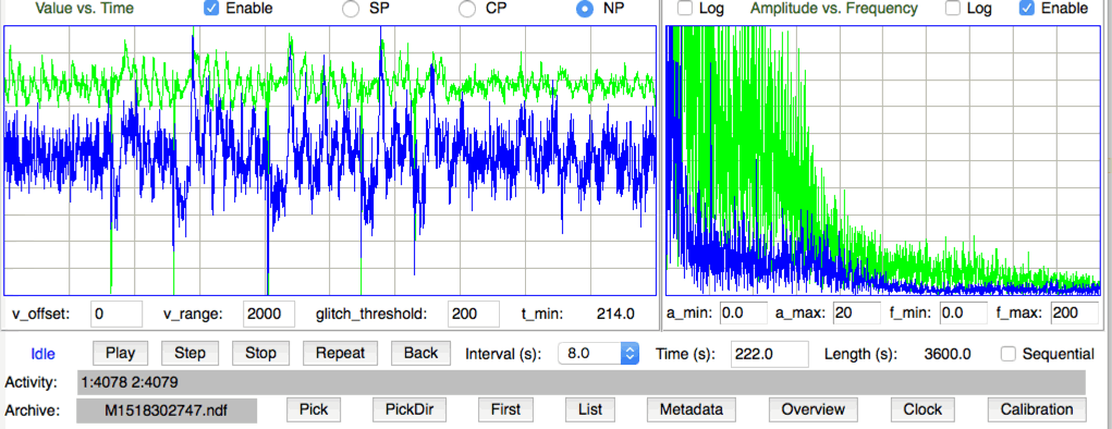
Judging by the frequency response, we are guessing that this is an A3028J-AAA. We see switching noise of amplitude 5 μV rms.
[15-FEB-18] We receive M1513090524.ndf from Edinburgh University, a recording made of intercostal muscles using an A3028B. We see heartbeat and respiration.
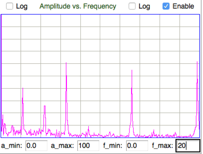
The heartbeat fundamental is at 6.3 Hz, with harmonics at 13 Hz and 19 Hz. Respiration fundamental is at 2.1 Hz with harmonic at 4.2 Hz.
[27-FEB-18] We have first article, 5 pieces, of A3028PV1. Here is the bottom side of the board:

We connect 2.7 V to the circuit and de-activate. Quisecent current fluctuating 0.5 to 1.0 μA. We look at VB and find the following 29-mV pulses with period 260 ms.

We put a 1000-μF electrolytic capacitor across VB. After a while we measure a stable current of 0.8 μA. We disconnect the circuit and after a minute the capacitor itself draws 0.0 μA. Inactive current is 0.8 μA. We program with P3028P01 but oscillator U10 is not producing any signal, just 0V, and current is 400 μA. We set up a ring oscillator between TP1 and TP2 and see 131 MHz, current now 6.2 mA. It turns out we should set all inputs to HOLD, including those that we have used as layout bridges to power and ground pads within the BGA footprint. Having done this, active current is 24 μA. We have no RCK. We try a third assembly with the updated firmware and it works fine. With 512 SPS on X, current consumption is 70.4 μA. We re-program as A3028P, 128 SPS, 0.3-40 Hz, and see active current consumption 30 μA. We obtain the following frequency response with a 20-MΩ 5-mV sweep.

We see a half-power frequency of about 45 Hz, with which we are well-satisfied. At 30 μA, expected operating life with a 30-mAhr CR1025 battery will be 1000 hrs. With 0.8 μA quiescent current, shelf life will be 52 months.
We have batch B200_55 consisting of 11 of A3028B-AA. Frequency response B200_55 within ±0.3 dB. Noise ≤12 μV in all, with some as low as 6 μV rms total noise from 1-160 Hz. Switching noise fundamental amplitude ≤4 μV in 37 °C water.
[28-FEB-18] We have batch B200_62 consisting of 12 A3028B-AA. Volume of nine bodies measured together by displacement in a beaker of water is 12 ml, making individual volume ≈1.3 ml. response B200_62 within ±0.3 dB. Noise <8 μV from 1-160 Hz. Switching noise fundamental amplitude ≤3.5 μV in 36 °C water.
[06-MAR-18] We place B200.78, 81, and 82 in the oven at 60°C to poach. We check their frequency response first with 20-MΩ sweep, and find it correct. We have B207.3 and 10 with epoxy before dipping in silicone and we find that they don't turn on. They consume 16 mA from an external supply. We observe 1V8 = 0.0 V and VD = 0.2 V. We believe there is a short under the logic chip from 0V to 1V8.
We remove U10, the oscillator, from an A3028PV1 assembly and program. When we turn on power to the logic and amplifiers, current consumption is 15 μA. We program two more complete A3028PV1, but in both cases U10 does not work, and current consumption is 50-100 μA. We attempt to replace U10 on three assemblies, each of which consume 15 μA without U10. We succeed temporarily in some cases, but cleaning and drying eventually reveal a bad joint under the BGA-4 package. We give up. We erase the logic chip on our single working assembly. We reprogram. We repeat. We try OFF for the pull-up setting and find that does not reduce current. We go back to HOLD. The board is still working fine, drawing 30 μA. We now suspect that U10 was broken during assembly.
[09-MAR-18] Poaching transmitters B200.78, 81, and 82 100% reception, response to 20-MΩ sweep correct. We have batch B207_1 consisting of twelve A3028B-AA. Two failed after epoxy encapsulation. We found they consumed 16 mA when active, and trace this drain to the logic chip, which is shorting the 1V8 power supply. Now we have nine left, after burn-in and three-day soak. Frequency response B207_1 within ±0.3 dB. Switching noise in 37°C water ≤3 μV, total noise ≤7 μV rms.
[12-MAR-18] Poaching transmitters B200.78, 81, and 82 100% reception, response to 20-MΩ sweep correct.
[14-MAR-18] Poaching transmitters B200.78, 81, and 82 100% reception, response to 20-MΩ sweep correct.
[15-MAR-18] Poaching transmitters B200.78, 81, and 82 100% reception, response to 20-MΩ sweep correct.
[16-MAR-18] Poaching transmitters B200.78, 81, and 82 100% reception, response to 20-MΩ sweep correct. We have 15 of A3028PV1 from assembly house. We program, calibrate, and test. Thirteen work perfectly. Active current consumption is 32 μA on average. Two have a fault with U10, the BGA-4 oscillator, circuits 0006 and 0015. There is no CK output and current consumption is 200 μA. We see nothing wrong with the way the chips are soldered. Below is bottom side-view of

We have batch B205_6 consisting of ten A3028B-DD and three A3028B-AA. Frequency response B205_6.gif within ±0.3 dB. In water at 37°C we see rumble on the DD transmitters, but <6 μV on the AA. After ten minutes, noise on the DD is still 50 μV or more. We scrub all the pins. Now we have noise <8 μV on all DD and noise <6 μV on the AA. Switching noise fundamental is ≤3 μA and second harmonic is ≤1.5 μV. Two have wrinkles in silicone following a failure of our heating system earlier this week. We reject these, leaving sufficient to complete the job. We put B205.9 and B205.13 in the oven to poach at 60°C.

We load batteries onto two non-functioning A3028PV1 circuit boards. We solder the positive terminal directly to the edge of the battery. We connect the negative terminal with a bent copper wire.
[19-MAR-18] All five poaching transmitters 100% reception and correct response to 20-MΩ sweep.
[20-MAR-18] All five poaching transmitters 100% reception and correct response to 20-MΩ sweep.
[21-MAR-18] All five poaching transmitters 100% reception and detect heartbeat.
[22-MAR-18] All five poaching transmitters 100% reception and correct response to 20-MΩ sweep. We have E206.110 failed after epoxy encapsulation. Dissect. VB = 0.5 V. Disconnect VB = 1.2 V. Connect external 2.6 V. Inactive 1.4 μA, active 190 mA. With 1.0V supply we still see 11mA, with 1.5V, 50 mA. Remove U4, 1.5V gives 50mA. Diagnosis: short from VD to 0V running through U1's channel resistance S3028E_1. We check a bare circuit that failed QA with 500 μA current consumption. It runs fine, except for this consumption from VD. We clean vigorously with hot pressurized water, no change.
We receive back from assembly house two A3028PV1 upon which U!0, the oscillator, produces no signal. Of one of the balls under U10-3 were broken off at the chip, we would expect the fault to be affected by pressing on the chip. We tried pressing on the chip but saw no change in current consumption nor a start-up of oscillation. Here is a side x-ray of one of the two U10s provided by our assembly house.

We remove the two oscillators by heating with a solder blob until they come off onto the blob. We place them top down on paper and look at them through a microscope. Ball U10-3 appears to have broken off in both cases, while the other balls are either still adhered to U10 or have come off when liquid. We soak in hot water to remove flux and obtain the following photograph.

We note that U10, when deprived of VDD = 1.8 V is drawing up to 500 μA from U8 through U10-2 (see S3028P. After removing U10, both circuits consume only 15 μA. It is possible that both U10s have been damaged by U8 through U10-2. Subsequent mechanical connection of 1.8V to U10-3 through its broken solder ball does not start oscillation nor reduce current consumption. Broken solder balls like this were a persistent problem with our old BGA-5, as we described in 18DEC13
[27-MAR-18] All five poaching transmitters 100% reception. Response to 20-MΩ sweep is within 1 dB of correct for all but B200.81, which is 3 dB too low at 100 Hz. Response to 100-kΩ sweep is, however, within 1 dB for B200.81. Total noise ≤8 μV for B200.78, B200.81, and B200.82, which have bare wire electrodes, and ≤16 μV for B205.9 and B205.13, which have soldered pins. We remove the soldered pins and expose bare wire. Now the noise is ≤8 μV. The characteristics below give channel number, battery voltage, and noise in 2-160 Hz for a typical eight-second interval.
M1522157467.ndf 870.0 9 2.68 8.2 13 2.62 8.2 78 2.60 6.3 81 2.57 6.2 82 2.48 6.1
Battery voltage for the older three transmitters 78, 81, and 82 is 0.1 V lower than for the younger two. The older transmitters have been running for 500 hours. We expect them to run for another 120 hours.
We have batch E206_103 consisting of fifteen A3028E-AA made with A3028RV3 circuits. Response to 20-MΩ sweep E206_103 within ±0.3 dB. Total noise 2-160 Hz in 44°C water is ≤15 μV with switching noise fundamental ≤5 μV. We have batch B207_12 consisting of four A3028B-AA made with A3028GV1 circuits. Response to 20-MΩ sweep B207_12. In 39°C water, total noise 2-160 Hz is ≤10 μV, switching noise fundamental ≤4 μV.
[30-MAR-18] Poaching transmitters B200.78, B200.81, and B200.82 show some activity with low battery voltage when hot, but turn off when they cool down. It has been 580 hrs, which is within 10% of the expected 620 hours. Diagnosis: full life. Poaching transmitters B205.9 and B205.13 response to 20-MΩ sweep correct, 100% reception.
We have two physical prototypes T1 and T2 of the A3028P. Both are equipped with 0.5±0.1 mm leads and an antenna made of a 0.7±0.1 lead.

Prototype T1 has one thick coat of epoxy with no touch-up and three coats of silicone. Its weight is 1.5 g. Its maximum thickness is 5.2 mm, minimum 4.5 mm. Estimated volume 0.9 ml. Prototype T2 has one thin coat of epoxy followed by touch-up and two coats of silicone. Its weight is 1.4 g. Its maximum thickness is 4.6 mm, minimum 3.6. Estimated volume 0.75 ml.
[02-APR-18] Poaching transmitters B205.9 and B205.13 response to 20-MΩ sweep correct, 100% reception. Battery voltages around 2.6V. No rumble in signal. Both were off when we took them out of the oven. We may have turned them off on Friday.
[04-APR-18] Poaching transmitters B205.9 and B205.13 100% reception and detect heartbeat.
[05-APR-18] Poaching transmitters B205.9 and B205.13 100% reception, response to 20-MΩ sweep correct. Battery voltages at 25°C 2.38 V and 2.50 V respectivey.
[06-APR-18] Poaching transmitters B205.9 and B205.13 100% reception, response to 20-MΩ sweep correct. Battery voltages at 60°C 2.66 V and 2.62 V respectivey. We have batch B200_83 consisting of 22 of A3028B-AA with 45-mm leads. Volume of 9 together is 12 ml, average 1.3 ml. We change our amplifier gain comparison range from 1-130 Hz to 0.25-160 Hz. With this extended range, the amplifiers agree to ±1.3 dB, which is within a 3-dB spread, see B200_83. In water at 37°C total noise in 2-160 Hz is ≤11 μV. Switching noise fundamental ≤4 μV.

Of the 22, all pass quality control, but if we remove B200_85 and B200_91 we have maximum noise 9 μV and amplifier agreement ±0.9 dB, so we set them aside.
[09-APR-18] Poaching transmitters B205.9 and B205.13 100% reception, response to 20-MΩ sweep correct. Battery voltages at 30°C 2.38 V and 2.41 V respectivey.
[10-APR-18] Poaching transmitters B205.9 and B205.13 100% reception, response to 20-MΩ sweep correct. Battery voltages at 50°C 2.48 V and 2.53 V respectivey.
[11-APR-18] Poaching transmitters B205.9 and B205.13 100% reception, battery voltages at 55°C 2.45 V and 2.57 V respectivey.
[12-APR-18] Poaching transmitter B205.9 has stopped. B205.13 100% reception, battery voltage at 60°C 2.53 V. Response to 20-MΩ sweep correct.
[13-APR-18] Poaching transmitter B205.13 has stopped. We have batch E206_121 consisting of sixteen A3028E-AA. Gain versus frequency within ±0.7 dB in 0.2-160 Hz, see E201_121. We measure volume of bodies plus antennas and 30 mm of leads for 16 transmitters, avearge volume is 3.3±0.1 ml. We measure volume of 4 bodies to be 12 ml, or 3.0 ml each. These transmitters we allowed to drain of epoxy for less time than usual, resulting in more epoxy on the device, increasing their volume by approximately 0.2 ml. Noise in water at 45°C is ≤9 μV with switching noise fundamental ≤3 μV.
[17-APR-18] We put E206.130 in the oven to poach at 60°C. This device transmitted all zeros for a few minutes during quality control, so we rejected it.
We cut back the antenna of an A3028P transmitter from 50 mm to 5 mm, sealing the end after each cut with an acrylic coating. We immerse the transmitter in the same location in the center of a 250-ml beaker of water 25 cm from an A3015C loop antenna. We use our spectrometer to measure power received by the antenna.

We place the A3028P with 5-mm sealed antenna up against the glass in a beaker of water in our faraday enclosure with one receiving antenna (position A). We obtain 100% at all locations on our ALT platform. Of 30 random locations in the enclosure, we obtain 100% reception in half, >90% in thirteen, and <20% in two. With two receive antennas we obtain 100% reception everywhere. We drop the transmitter in the bottom of the beaker, so it is horizontal (position B). We obtain 100% reception in 19 of 20 locations and 50% in 1 of 20.
We cut off the antenna entirely and seal with silicone. We cut back the 50-mm antenna on another A3028P to 20-mm. We place both transmitters in position A. We place on the ALT platform and move and rotate at random. We obtain 31% reception from the 20-mm antenna and 69% from the 0-mm. We compare an A3028E with 50-mm loop antenna in position B, an A3028P with 0-mm in A and an A3028P with 15-mm in A, recording simultaneously with one antenna. We get 100.0%, 93.7% and 76.5% reception respectively. We cut back the 15-mm antenna to 10 mm and repeat. We get 96% from the A3028E, 88% from the 10-mm and 55% from the 0-mm. We cut back the 10-mm to 5 mm. We get 99.1% from the A3028E, 98.1% from the 5-mm and 61% from the 0-mm.
[20-APR-18] We repeat the above experiment with the same transmitters in the same positions, but the beaker is empty. We get 99.9% from the A3028E, 54.7% from the 5-mm and 0.9% from the 0-mm. We pour water in and repeat. We get 99.9% from A3028E, 98.3% from 5-mm and 61.7% from 0-mm. We load a new 13-mm antenna in place of 0-mm. We try A3028E in water B, A3028P 5-mm in water A and 13-mm outside the wall of the beaker, in air, position C. We have double-coated the 5-mm antenna in acrylic to make sure it's isolated. We get 98.8% from A3028E B, 92.3% from 5-mm A, 92.8% from 13-mm C. We double-coat the 13-mm in silicone and place it in water along with the 5-mm in position A. We get 99.5% from A3028E, 91.7% from 5-mm and 99.0% from the 13-mm. We empty the beaker, leaving A3028E in B and the 5-mm and 13-mm antennas in C. We get 99.9% from A3028E, 61.4% from 5-mm, and 95.1% from 13-mm.
The 13-mm antenna gives us over 90% reception in air, in water, or near water. We connect two antennas inside our enclosure and measure reception from A3028E in water B and 5-mm and 13-mm antennas in water at A. We get 99.9% from A3028E, 99.3% from 5-mm, and 98.0% from 13-mm.
[23-APR-18] Poaching transmitter E206.130 100% reception, VB = 2.77 V, response to 20-MΩ sweep correct.
[26-APR-18] Poaching transmitter E206.130 100% reception, transmits all zeros as it did during quality control.
[27-APR-18] We have batch E200_107 consisting of sixteen A3028E-FB, one coat SS-5001 and one outer coat of MED-6607. Frequency response E100_207 within ±0.8 dB. Switching noise in 35°C water ≤3 μV, total noise ≤11 μV.
[30-APR-18] Poaching transmitter E206.130 still running 100%, transmits all zeros.
[01-MAY-18] We have batch B206_139 consisting of 12 A3028B-AA. Volume of 8 together is 10.0 ml, or 1.25 ml. Frequency response B206_139 within ±0.5 dB. Total noise in 37°C water is ≤8 μV, switching noise fundamental ≤4 μV.
[07-MAY-18] Poaching E206.130 100% reception, transmits all zeros. Add to poach P90, prototype pup transmitter, and E200.119.
[10-MAY-18] Poaching E206.130 100% reception, transmits all zeros. P90 and E200.119 response to 20-MΩ sweep correct, 100% reception.
[14-MAY-18] Poaching E206.130 100% reception, transmits all zeros. P90 and E200.119 response to 20-MΩ sweep correct, 100% reception. Noise <8 μV, switching fundamental <1 μV in 60°C water.
[15-MAY-18] Poaching E206.130 100% reception, transmits all zeros. P90 and E200.119 response to 20-MΩ sweep correct, 100% reception. P90 VB = 3.01 V, E200.119 VB = 2.83 V.
[16-MAY-18] Poaching E206.130 100% reception, transmits all zeros. P90 and E200.119 response to 20-MΩ sweep correct, 100% reception. P90 VB = 3.01 V, E200.119 VB = 2,83 V. We see red and white corrosion inside the silicone at the base of the leads and antenna, especially where we burned away the epoxy to re-solder the antenna before re-applying silicone.
[18-MAY-18] Poaching E206.130 transmitting X again. All three E206.130, E200.119, and P90 response to 20-MΩ sweep correct and 100% reception. P90 VB = 2.95 V, E200.119 VB = 2.82 V, E206.130 VB = 2.84 V.
[21-MAY-18] Poaching E206.130, E200.119, and P90 response to 20-MΩ sweep correct and 100% reception.
[22-MAY-18] Poaching E206.130, E200.119, and P90 response to 20-MΩ sweep correct and 100% reception.
We have batch P1_89 consisting of 11 of A3028P-AA. Frequency response P1_89 within ±0.5 dBm. Noise ≤4 μV in 2-100 Hz. Transmit center frequencies in range 913-918 MHzz. We have three breaches in the silicone, which is too thin. We dry out and add another coat of silicone, making three coats total.
[24-MAY-18] Poaching E206.130, E200.119 response to 20-MΩ sweep correct and 100% reception. P90 100% reception and amplifiers and filters still working, but the baseline signal is swinging around, with bumps a few times a second.
[25-MAY-18] Poaching E206.130, E200.119 response to 20-MΩ sweep correct and 100% reception. P90 100% stops transmitting. We find that its antenna has corroded through at the base under our failed silicone patching. Even the antenna pad has corroded all the way through the circuit board, and the X− lead beside the antenna. Battery voltage 2.2 V. External 2.7 V, inactive 0.8 μA, active 19 μA. Diagnosis, Faulty Encapsulation.
[29-MAY-18] Batch P1_89 consisting of 12 of A3028P-AA now has three coats of silicone. No sign of rust or corrosion after five-day soak. Total noise in 0.5-40 Hz is ≤3.5 μV. No trace of switching noise. Reception 100%. Volume of 10 pieces is 6.0 ml. Mass is 1.41±0.01 g.
We add P1.89 to poach. It has three coats of MED-6607 and a 5-mm helical antenna. Poaching transmitters P1.89, E200.119, E206.130 battery voltages 2.92 V, 2.83 V, 2.81 V and reception 100% in water. Response to 20-MΩ sweep correct.
[01-JUN-18] We receive 30 of A3028PV1, build B76438. We test 26, 9 work. Of the 17 that fail, 2 have U10 working but consume excessive current (9 mA in No17, 0.11 mA in 07) until we remove U10, ASTMTXK, then current drops to 15 μA. Another 2 have the oscillator frequency varying with time, 4-6 kHz gradually, then fluctuating rapidly (22 and 11). The remaining 13 have U10 generating no signal and consume 30-300 μA. We remove U10 from half of these and current in every case drops to 15 μA. We re-program and feed 32.768 kHz in through TP1 and all these boards work perfectly. Of the 9 that work, 2 end up consuming 85 μA and 95 μA so we remove U10 and reprogram to show that U10 was responsible for the excessive current.
[04-JUN-18] With new magnifiers, we load new U10 onto five A3028PV1 circuit boards, dry, and calibrate. Current consumption 73.5-77.7 μA. Poaching transmitters P1.89, E200.119, E206.130 reception 100%, response to 20-MΩ sweep correct.
[05-JUN-18] We replace U10 on another 11 of our A3028PV1 circuit boards and all are now working. We cannot replace U10 on 3 boards because the solder mask over the track leading from U10-3 has come off and the exposed coper wicks the U10-3 solder ball all the way to U4-3. We revive two boards from the previous build and they work. We are left with 4 un-touched boards, 2 with fluctuating oscillators, and 23 working. We take a working board and erase the logic chip, but U10 still works. If we drive U10's output with the logic pin, current consumption increases bny 200 μA but U10 works after re-programming. We hear from assembly house, "We suggest running using a LeadFree profile and Leaded solder if they want to continue using this part. Additionally we will place notes for handling glass parts on this board. If this is sufficient then we will need to notify ENG to update paperwork."
We have batch D208_157 consisting of 12 of A3028D-DDA. Frequency response D208_157 within 0.5 dB, noise 2-160 Hz <10 μV, switching noise <3 μV.
[08-JUN-18] Poaching transmitters E200.119 and E206.130 still running, but P1.89 has stopped.
[11-JUN-18] Poaching transmitters E200.119 and E206.130 100% reception and response to 20-MΩ sweep correct. Dissect P1.89. Silicone well-adhered. No signe of corrosion. VB = 0.1 V. Disconnect, VB = 0.1 V. Connect external 2.7 V. Inactive 0.8 μA, active 34 μA. Reception 100%. Response to 20-MΩ sweep correct. Diagnosis "Unidentified Drain".
[15-JUN-18] Poaching transmitters E200.119 and E206.130 100% reception and response to 20-MΩ sweep correct for E200.119, but 6 dB too low at all frequencies for E206.140. VA = 2.81 and 2.74 V respectively.
[19-JUN-18] We equip 5 of A3028P3 bare circuits with fresh CR1025 batteries soldered to the boards with a wire and a solder joimnt on the side of the battery. The transmitters each have 20-mm antennas. We place them in our big faraday enclosure. The A3028P3 runs at 512 SPS and its current consumption is around 75 μA. We expect 400 hrs of operating life. See below for final result.
Poaching transmitters E200.119 and E206.130 100% reception, VA = 2.84 and 2.78 V respectively at 60°C. E200.119 response to 20-MΩ sweep correct. E206.130 response to 20-MΩ sweep 20 dB too low, response to 50-Ω sweep correct.
We unpack 3 of our A3028PV1 assemblies. We connect 2.6 V and scrape the solder mask from the track leading between U10 and U8. In 2 circuits we see a 1.8-V, 32.7 kHz square wave. In 1 circuit we see 0 V. We program all three boars. We see 85 μA and 95 μA operating current in the first two boards, with the 32.7 kHz appearing on TP2. We see 29 μA on the third board, with no 32.7 kHz. The nominal operating current is 75 μA. With the oscillator removed we expect 15 μA. These three examples of U10 are consuming 10 μA, 20 μA, and 14 μA.
We receive recording of baseline and picrotoxin seizures from an adult mouse with an A3028P-AA implanted at ION/UCL. Baseline amplitude is 40 μV rms. Seizure spikes 1 mV, see here. Average reception in two hours of recordings is 98% with 97% of intervals having ≥80% reception.
[22-JUN-18] We have batch B202.43 consisting of 9 A3028B-DA. We add B200.85 to make ten. Frequency response B200_43 is within ±0.4 dB. Total noise 2-160 Hz in 37°C water after scrubbing pins is ≤10 μV, switching noise ≤5 μV. But B202.49 shows intermittent steps of several millivolts, even after scrubbing the leads twice and isolating it in its own beaker. We find a strand of antenna wire sticking through the silicone.
[25-JUN-18] We have B204.49 after removing stray wire and coating twice with silicone over the cut end. We place in water at 37°C. We scrub the lead tips. No sign of the intermittent steps we saw earlier. Noise is 10 μV rms 2-160 Hz. Removce from water and place in air. See no rumble. Noise is 9 μV.
We send four ASTMTXK oscillators back to the manufacturer, here they are arranged on a gel back with symptoms listed, as observed when they arrived from assembly house, and a few weeks later. The balls are no longer intact on the bottom of each BGA-4, but we make sure each pad has a coating of solder.

[03-JUL-18] We have batch P204.140 consisting of three A3028P3-AA. Frequency response P204_140 correct, noise ≤6 μV in 2-160 Hz, switching noise <0.4 μV.
[04-JUL-18] We have batch B207_18 consisting of fifteen A3028B-AA. When we have added a drop of silicone to cover the tips of the antenna wires, and in a few cases this drop has a cavity, but the problem is cosmetic only. Frequency response B207_18 with ±0.5 dB. Switching noise in 37°C water ≤3.2 μV, total noise 2-160 Hz ≤8 μV.
Poaching transmitters E200.119, E206.130 reception 100%. E206.130 VA = 2.7 V. E200.119 response to 20-MΩ sweep correct, VA = 2.85 V.
[19-JUL-18] Poaching transmitters E200.119, E206.130 reception 100%. E206.130 VA = 2.62 V. E200.119 response to 20-MΩ sweep correct, VA = 2.78 V. Our discharge of five CR1025 batteries by five A3028P3 circuits is complete. Average battery life it 400 hrs, expected is 400 hrs, range is ±2.5%.
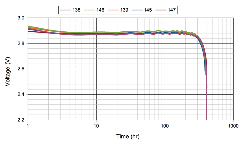
[24-JUL-18] Poaching transmitters 100% reception. We have batch B202.56 consisting of 11 of A3028B-DA. Frequency response B202_55 within ±0.7 dB, switching noise in 37°C water ≤3.5 μV, total noise ≤12 μV (there are pins soldered to the lead tips). We can see the red top side of the circuit board at the corners, the epoxy is so thin. But silicone coating is firm.
[27-JUL-18] Poaching transmitters E200.119, E206.130 reception 100%. E206.130 baseline fluctuating. E200.119 response to 20-MΩ sweep correct, VA = 2.75 V. We add four of A3028B to poack: B200.91, B202.61, B207.30, B207.33, and B207.34.
[31-JUL-18] Poaching transmitters B200.91, B202.61, B207.30, B207.33, and B207.34 reception 100%, response to 20-MΩ sweep correct, VA = 2.68±0.1 V, noise <7 μV, except for No91, which is 11 μV. Poaching transmitter E206.130 reception 100%, fluctuating baseline. E200.119 stopped. Dissect. VB = 2.63 V. Disconnect battery, VB = 2.92 V. Connect external 2.6 V, active current 960 μA, inactive 1.7 μA. We find that VB = 2.63 V but VA = 2.27 V, suggesting 360 μA through R4. Heat up C4 and now current is 310 μA, 1V8 = 1.8 V. Sleep-wake and current is 969 μA again, but 1V8 = 1.8 V still. VC = 1.8 V. Clear epoxy from around C3 and U9-8 with intent to measure VD. But now the transmitter draws 80 μA and we receive from channel 130. Soon after, it's back to 960 μA and VD = 2.6 V. Now VA = VB = 2.6 V, !SHDN = 0V, TUNE = 0.44 V and VA = 2.3 V. The logic chip is getting stuck in one of its transmit states. Pull off battery. Active 81 μA, reception 100%. Connect external battery. Response to 20 MΩ sweep 10 dB too low but otherwise correct. Check CK and find its period is 32.8 kHz and 0-1.8 V logic levels. There is a cavity in the epoxy between U9-3, C13, and R13. Diagnosis "Transmit Malfunction".
[03-AUG-18] Poaching transmitters B202.61, B207.30, B207.33, and B207.34 reception 100%, response to 20-MΩ sweep correct. B200.91 has stopped. Cannot turn it on. E206.130 reception 100%, fluctuating baseline.
[06-AUG-18] Poaching transmitters B202.61, B207.30, B207.33, and B207.34 reception 100%, response to 20-MΩ sweep correct. E206.130 has switched itself off, can turn it on again. Dissect B200.91. Silicone well-adhered. No cuts or cavities. No sign of corrosion. VB = 0.2 V. Disconnect VB = 0.2 V. Connecct external 2.7 V. Inactive 2.8 μA. Active 83 μA. Recaption 100%, response to 20-MΩ sweep correct. Later, inactive current is 2.0 μA and active current is 78 μA.
[07-AUG-18] Poaching transmitters B202.61, B207.30, B207.33, and B207.34 reception 100%, response to 20-MΩ sweep correct. B200.91 active 78 μA, inactive 2.0 μA. Dissect E206.130. Silicone well adhered. No sign of corrosion. VB = 2.8V. Connet external 2.7 V. Active 85 μA, inactive 1.7 μA. Diagnosis "Temporary Shutdown". Repair three of four A3028PV1 circuits by loading SiT1552 for U10. We load a total of four chips and all four work. One we replace because the U10-1 ball was missing, but it worked anyway. The fourth board we could not fix because solder mask is missing from U10-3 to U4 and the track wicks away the ball.
[16-AUG-18] Poaching transmitters B202.61, B207.30, B207.33, and B207.34 reception 100%, response to 20-MΩ sweep correct. A3028P1 transmitter No97 equipped with 0.5-mm wires has been implanted in an adult mouse at ION since 18-JUN-18, but left off. On 30-JUN, 08-AUG, and 09-AUG we turn on the transmitter for a few hours and it records EEG. We receive this report from manufacturer of ASTMTXK oscillator, which we use for U10 in the A3028P devices, showing physical damage to the part around the solder balls, which suggests that the devices were damaged by the pick and place machine. We will have these parts hand-placed in our next assembly job. We receive fine recordings of cortical spreading depressions (CSDs) following seizures in adult mice using our DC-160 Hz A3028U transmitters.
[17-AUG-18] We have batch C206_157 consisting of 11 of A3028C-CC. Frequency response C206_157 within ±0.7 dB, switching noise fundamental ≤3 μV, total noise ≤8 μV.
[20-AUG-18] Poaching transmitters B202.61 and B207.30 have stopped. B207.33 and B207.34 100% reception, response to 20-MΩ sweep correct for No33, 6 dB too low for No34. Battery voltages 2.52 V.
[21-AUG-18] B207.33 and B207.34 have stopped. We have three A3028T1-R, 0.3-40 Hz with A3028PV1 circuit and ML621 Li-Mn battery 6.8 mm in diameter. We measure battery voltage and get 2.66 V, 2.66 V, and 2.60 V. Looking at our discharge plots, it looks like the batteries are over 90% full. We connect the first one to 3.2 V through 400 Ω and see 400 μA flowing in with 2.92 V across the battery. After a few minutes, disconnect and see battery voltage 2.72 V.
[31-AUG-18] We have batch T209_1 consisting of three A3028T1-R. Frequency response T209_1 correct. Switching noise in 37°C water ≤3 μV, total noise ≤6 μV, see spectrum. Battery voltages 2.55 V, 2.49 V, and 2.46 V. Looking at discharge curves for the ML621 we conclude we must top up the charge of all three devices. We connect T209.1 and T209.2 through 1 kΩ and a microammeter to 4.2 V. Both are turned off. Each draws 130 μA separately, and together they draw 240 μA. If we turn either transitter on, it draws up to 500 μA with full-scaled steps on X. We leave to charge with 4.0 V connected directly to the 1-kΩ charging resistor.
[04-SEP-18] Devices T209.1 and T209.2 have been charging for four days. Current from 4.0 V through 1.0 kΩ is now 6.2 μA. Assuming 3 μA into each device, the charging diodes will each drop 0.45 V, so the voltage on the battery should be around 3.1 V. We place them both in water with T209.3. Battery voltages are 3.24 V, 3.17 V, and 2.41 V respectively. Noise at 25°C is 4.3 and 4.2 μV with switching noise <1 μV. Connect T209.3 to 4.0 V through 1 kΩ and see 90 μA flowing in. Leave to charge up.
[06-SEP-18] Our A3028T1, T209.3 is charged to 3.15 V. We have recorded its charge current with time from a 4.0-V supply through a 1-kΩ resistor.

We leave T209.1 running in our faraday enclosurefrom 9:30 am 06-SEP-18.
[10-SEP-18] Our A3028T1 T209.3 battery voltage is 2.2 V. Response to 20-MΩ sweep correct.
[11-SEP-18] Our A3028T1 T209.3 battery voltage is 2.14 V. Response to 20-MΩ sweep correct, but we must perform the sweep with a 5-mVpp sweep rather than 10-mV sweep because the dynamic range is now −17…+4 mV. Transmitter has been running for 127 hours.
[12-SEP-18] Our A3028T1 T209.3 battery voltage is 2.05 V. Response to 20-MΩ sweep correct. Transmitter has been running for 144 hours.
[14-SEP-18] Our A3028T1 T209.3 has stopped. Our recording shows battery voltage 2.00 V after 150 hours. We charge the battery from 4.0 V through 1 kΩ. We have batch P207_35 consisting of 17 A3028P1-AA. Volume of all seventeen including leads and antenna is 11 ml, making individual volume 0.65 ml. Response to 20-MΩ sweep P207_35 within ±0.6 dB. Total noise ≤5 μV rms, switching onise ≤0.6 μV. One of the fifteen, P207.49, won't stay on.
[19-SEP-18] We place P207.41 and P207.45 in the oven to poach at 60°C. Battery voltages are both 2.96 V. Both are P3028P1-AA, but P207.41 required re-work after epoxy encapsulation, burning away epoxy to re-attach the X+ lead.
[24-SEP-18] Poaching transmitters 100% reception. P207.41 has wandering baseline and does not respone to frequency sweep. P207.45 correct response.
[26-SEP-18] Batch B206_190 consists of four devices, two new and two previously checked. Frequency response B206_190 correct, noise ≤8 μV, switching noise ≤4 μV at 35°C. Poaching transmitters 100% reception. P207.41 has wandering baseline and does not respone to frequency sweep. P207.45 correct response.
[28-SEP-18] We have three A3028T1-R encapsulated with epoxy that fail quality assurance. T209.7 lost its X lead. The other two fail to transmit. The two that fail to transmit both have the same problem: the battery cannot supply 32 μA of operating current. Its voltage drops to 1 V. When supplying the inactive current of 0.8 μA, its voltage is 2.2 V. We connect 3.2 V through 1 kΩ directly to battery T209.6 and see only 7 μA flowing in. Battery T209.11 accepts a 90-μA recharge current. Its battery voltage is 3.1 V. As soon as we disconnect the charging voltage, the battery voltage drops to 2.2 V. We connect 4.0 V through 1 kΩ to the X leads of T209.7 and see 1 mA flowing in.
We take the same ML621 with solder tabs we used for our ML-series recharge experiments. Its votltage is 3.00 V. Apply 500°F iron for ten seconds, clean off flux with water, now 2.92 V. Repeat, voltage 2.86 V. Repeat, and after 9 s the battery voltage drops suddenly to zero. Take out a fresh ML621 from its package. Measure 2.78 V. Apply 500 F and after 10 s the battery voltage drops to 0 V. Apply 500°F for 3 s on, 3 s off, on fourth heating, battery voltage drops to zero. We take a fresh ML621. We load it with 1 kΩ for ten seconds. Its voltage is 2.67 V. We load with 1 kΩ. Voltage drops immediately to 2.49 V, implying output resistance 72 Ω. After one minute, 2.32 V. Disconnect, after five minutes battery has recovered to 2.69 V. Apply 500°F for three seconds, 2.72 V. Apply 1 kΩ, drops to 2.58 V, implying 56 Ω. Apply 500°F for 3 s again, 60 Ω. Apply 500°F for 14 s and voltage goes to 0.00 V. We notice a sweet smell. The plastic ring that separates the terminals has bulged up and out of its slot. The failure is a sudden short-circuit.

Another fresh battery, soldered by tabs to a circuit board, as shown above, has voltage 2.61 V before 1 kΩ load, 2.45 V immedaitely after, for 64 Ω. Short circuit for ten seconds, voltage recovers to 2.45 V after one minute. Apply 500°F to the cut-off battery tab on the 0-V terminal for 20 s, battery voltage stable at 2.58 V.

When we charge the ML621 through the X leads of an A3028T1R, we do so through the 65-Ω resistance of each of its two 27-mm leads, and two BAS116LPH4 diodes. At the end of a re-charge, the current is of order 4 μA. At 25°C, the diodes will each drop 0.5 V. The temperature in our laboratory is, however, closer to 20°C. According to our calculations, the diode voltage should be around 0.52 V, so both of them together are 1.04 V. When we apply 4.0 V, the voltage on the battery will be 4.0 V − 1.04 V − (1120 Ω × 3 μA) = 2.96 V. We have had success charging with 2.9-3.3 V in the past.
[02-OCT-18] Dissect T209.7. Active current consumption with external 2.6 V is 35 μA. Connect batterty. When inactive, voltage is 2.4 V, when active, 2.3 V. We charge battery directly with 3.2 V and 1 kΩ and see 20 μA. We charge with 4.0V and 1 kΩ on the X leads and see 1 μA. There appears to be 1.2 V across D1 with only 1 μA. Something is wrong with internal connections. We connect 20-MΩ 20-Hz 30-mV and see gain varying by a factor of two over the course of seconds. Dissect T209.18. Active 32 μA with external 2.6 V. Battery shows 2.4 V when inactive, dropping to 1.2 V when active. Charge with 3.3 V and 1 kΩ see 20 μA flowing in. Battery is damaged. Dissect T209.13. Active and inactive current 15 mA, no transmission. Battery drained to 1.1 V. Connect 3.3 V through 1 kΩ see 500 μA. After five minutes, disconnect charger and battery is at 2.6 V. Connect to circuit of T209.7 and we see transmission. Battery was drained by excessive current consumption of T209.13, but recovered.

The T209.7 device runs well, but only for 110 hrs after its first re-charge, and only for 75 hrs after its second re-charge. We connect it to 4.2 V to see if we can get it to a full 5 mA-hr. The remaining six discharge curves shown above are consistent with 160-hr operating life, if we accept that No8 and No9 batteries were discharged during assembly and encapsulation.
[03-OCT-18] Poaching transmitters 100% reception. P207.41 has wandering baseline and does not respone to frequency sweep. P207.45 correct response to 1-200 Hz 20 MΩ sweep.
[05-OCT-18] We have batch P206_171 consisting of 15 A3028P2-AA. Frequency response P206_171 within ±0.8 dB. Noise <5 μV, switching noise <0.5 μV. We identiy our copper spade-end alligator clips as the source of our problems while attempting to charge a set of eight A3028T1-R. We solder gold pins to the leads of one of the devices, but the contact is intermittene between the copper clips and gold or steel. We heated the copper clips with a 650°F soldering iron to assemble them into an eight-position charging fixture, but we see no visible sign of oxide on the surface. And yet the contact resistance varies with pressure and moisture. When measuring the frequency response of batch P206)_171 with these clips, we several times see gain 20 dB too low at 1 Hz rising to correct at 100 Hz, suggesting a contact that resists DC current. We replace all clips with tin-coated steel clips, the same we have been using for years, and all these intermittent problems cease, but we are left with the difficulty of grasping the 2-mil diameter stainless steel wire with such a clip.
[08-OCT-18] Poaching transmitters 100% reception. P207.45 VA = 3.0 V at 60°C, correct response to 1-200 Hz 20 MΩ sweep. P207.41 wandering baseline. Of the eight A3028T1-R we left charging over the weekend, 6 have charge current around 10 μA and two appear to have become disconnected. The 6 have VA 2.9-3.2 V when we turn them on. The 2 have VA = 2.5 V. We re-connect the 2 and see 40 μA flowing into each. We leave them charging. The 6 we leave to run in enclosure.
[09-OCT-18] We have batch Q206_190 consisting of 7 of A3028Q-DNA. We measure the thickness of the epoxy encapsulation and obtain an average value of 9.61 mm, and after one coat of SS-5001 and one coat of MED-6607 we get 11.24. So the silicone coat has thickness 0.82 mm. Frequency response Q206_193 within ±0.7 dB over 0.25-350 Hz, noise 2.0-320 Hz ≤10 μV, switching noise <0.5 μV. We see no switching noise peak in any channel. Poaching transmitters 100% reception.
[10-OCT-18] Poaching transmitters 100% reception. We examine the discharge curves for eight A3028T1-R we finished recharging two days ago, see here. Included in the plot are three discharges of the No3 device. The 72-hr discharge followed a recharge with 4V and copper clips, 112-hr followed 4V and steel clips, 116-hr followed 4.2V and steel clips. We are using only steel clips now. No4, 5, 10, 12, 14, 17 charged up to 2.9-3.3 V with 4.2V and subsequently their discharge remains above 2.5 V for 20 hours. No8, 9 charge to only 2.6V, even though their final charging current is 50 μA each. Their voltage does not rise farther. During discharge, they drop below 2.4V in ten hours. We reject No 8 and No9. We suspect they were damaged during assembly. We leave them to discharge further, and remove the other six, turn them off, and connect them to our group charger. Total charging current is 800 μA.
[12-OCT-18] Poaching transmitters 100% reception. P207.45 correct response to 1-1000 Hz 20 MΩ sweep. P207.41 wandering baseline. We have six of A3028T1-R-AA on our recharger, 4.2V supply with individual 1 kΩ resistors. Total charge current after 45 hours is 28 μA. We disconnect each in turn and so obtain final charge currents No10 7 μA, No5 0 μA, No12 1 μA, No17 14 μA, No14 4 μA, No4 2 μA. We reconnect No5 and find 100 μA flowing in. We do the same with No12 after running for ten minutes and see 10 μA flowing in. We connect No3, 8, and 9 rejected devices and see 300 μA, ≈1.3 μA and ≈1.3 μA flowing in to each. We leave No5 , 3, 8, and 9 charging. The remaining 5 are batch T209_4. Battery voltages 3.2-3.3 V. Total noise in 37°C water is ≤3.0 μA in 2-40 Hz, switching noise <0.6 μV. Frequency response T209.4 within ±0.2 dB.
[15-OCT-18] Charging transmitters T209.3, T209.5, T209.8, and T209.9 are together consuming 200 μA, 6 μA, 1.0 mA, and 1.0 mA respectively. T209.8 and T209.9 will not turn on. T209.3 and T209.5 turn on and produce VA = 3.1 V and 3.2 V respectively. We place these two in our faraday enclosure to run down their batteries. Poaching transmitter P207.41 has stopped. P207.45 response to 20-MΩ sweep correct, 100% reception. VA = 2.9 V.
[16-OCT-18] We dissect P207.41 after 26 days poaching. No sign of corrosion. Silicone well-adhered to epoxy, but peels off in one layer. VB = 0.15 V. Disconnect VB = 0.13 V. Connect external 2.7 V, Inactive 1.4 μA, active 38 μA, 100% reception, responser to 20-MΩ sweep correct. Diagnosis "Unidentified Drain". Dissect T209.9. VB = 2.1 V. Disconnect VB = 2.2 V. Connect external 2.7 V. Inactive 0.8 μV, ative 35 μV, 100% reception, response to 20-MΩ sweep correct. Connect 100 kΩ across battery, get 20 μA. Connect transmitter again, upon turn-on, VB drops to 1.0 V. Connect 1 kΩ and VB = 0.4 V. Diagnosis "Heat-Damaged Battery". Dissect T209.8. VB = 2.1 V. Disconnect VB = 2.2 V. Connect 100 kΩ to battery VB = 2.0 V, 1 kΩ VB = 0.3 V. Connect external 2.7 V to circuit. Inactive 0.8 μA, active 33 μA, 100% reception, response to 20-MΩ sweep correct. Diagnoisis "Heat-Damaged Battery". Poaching transmitter P207.45 100% reception, response to 20-MΩ correct, VA = 2.87 V. We have B206.193 with wrinkled silicone but otherwise okay, put it in oven to poach.
[19-OCT-18] Poaching transmitters P207.45 and B206.193 battery voltages 2.76 V and 2.70 V. Reception 100%, response to 20-MΩ sweep correct. We have batch C210.1 consisting of 12 of A3028C-AA. Frequency response C201_1. Switching noise in water at 41°C is ≤8 μV and total noise 2-80 Hz is ≤10 μV rms except for C210.7, which is 15 μV rms. The noise on C210.7 does not appear to be switching noise: there is no definite peak in the spectrum. But the noise consists of random 40-μV negative pulses. We add C206.157 (an older batch) and C210.7 to our poaching devices.
We have two sizes of Ag/AgCl electrode we purchased from A-M Systems. One is a 4-mm diameter 1-mm thick AgCl pellet with 70 mm of silver wire. The other is a 3-mm long 0.8-mm diameter AgCl pellet with 70 mm of silver wire. We solder the leads of an A3028Q transmitter as shown below.

We place the solder joints, silver wires, and pellets in room-temperature water. Input noise for 8-s intervals is typically 5 μV rms in 2-80 Hz. But we see movements below 2 Hz that are up to 200 μV, despite our 0.3-Hz high-pass filter.


We raise the solder joints out of the water leaving only the Ag/AgCl electrodes immersed. While the water is still rocking in the beaker, we see 2 Hz waves. When the water is still, noise in 2-160 Hz is 4.0 μV rms. Variation at lower frequencies is less than 2 μV. The following is typical of all intervals we record from water with two Ag/AgCl electrodes.

If we allow the solder joints to sit just outside the water, but partly wet, we see occasional steps of up to 20 mV on the input, which appear in the A3028Q signal as a step followed by a decay and overshoot with time constant roughly 0.5 s. We cut off one of the solder joints and strip the end of the stainless steel helix. We place the steel wire in the water along with the smaller pellet electrode to act as a reference on X&minusl;. We see movements below 2 Hz of much the same size and character as when we had the two solder joints immersed.
[22-OCT-18] Poaching transmitter P207.45 has stopped. Poaching transmitters B206.193, C206.157, and C210.7 reception 100%, response to 20-MΩ sweep correct. T209.3 and T209.5 both ran for over 140 hours. We connect T209.3 and T209.5 to our charger.

We continue our experiments with silver chloride electrodes. We first check our Ag/AgCl and 316SS electrode pair in water, and we see the same 200-μV rumble and steps we observed before. This time we take one Ag/AgCl electrode, which is an AgCl-coated pellet connected to a silver wire, and for the second electrode we provide another silver wire. Noise in 2-160 Hz is 3.8 μV and we see no rumble or steps. We cut off the Ag/AgCl pellet, leaving two silver wires in water. We see no rumble or steps. We immerse the newer solder joint in the water along with the new silver wire and see sustained pulses and rumble.
[23-OCT-18] We have three A3028T1R, T19-T21 made for poaching. These are made with the ML621 with tabs, so there is no over-heating of the battery during assembly. Their sample rate is 128 SPS but frequency response is 0.3-160 Hz. Mass of three is 3.04 g. Volume of all three is 1.45 ml. So mass of each is 1.0 g and 0.48 ml, consistent with our current 1.0 g and 0.50 ml specification. Response to 20-MΩ 60 Hz shows beats we expect from under-sampling. Connect to charger along with T209.3 and T209.5. Total charge current 620 μA.
We prepare 200 ml of 1% saline and immerse our two silver wires, attached to A3028Q No39, but with solder joints out of the water. We see 3.9 μV rms noise in 2-80 Hz. Rumble is less than 20 μV in 8-s intervals and there are no steps. We drop the entire transmitter in the saltwater, seal the jar, and place in our oven at 60°C.
Poaching transmitters B206.193, C206.157, and C210.7 reception 100%, battery voltages 2.71, 2.78, and 2.79 V respectively.
[24-OCT-18] Poaching transmitters B206.193, C206.157, and C210.7 reception 100%. Five charging A3028T1R transmitters drawing 150 μA total from 4.2 V charge voltage with 1 kΩ series resistors.
[25-OCT-18] Our five charging A3028T1R are consuming 53.5 μA. We remove them one by one. The final charge currents are 30 μA for T209.5, 3 μA for T21, 11 μA for T209.3, 4.5 μA for T20, and 5.4 μA for T19. We turn them all on and put them in our FE3AS to run their batteries down. Poaching transmitters B206.193, C206.157, and C210.7 reception 100%.
[26-OCT-18] Poaching transmitters B206.193, C206.157, and C210.7 reception 100%. Battery voltage and noise in 2-160 Hz are (id V uVrms): 7 2.78 5.2 157 2.73 6.2 193 2.69 6.0. Response to 20-MΩ sweep correct. Dissect P207.45. Silicone and epoxy in perfect condition. VB = 0.4 V. Disconnect VB = 0.4 V. Connect external 3.0 V. Active 31 μA, inactive 0.8 μA. This device ran for 800 hours. If we assume 32 μA, the CR1025 battery delivered 26 mA-hr. According to data sheets for MAX2624 and LC1865, current consumption at 60°C should be roughly 10% higher than at 20°C. We immerse the transmitter circuit in water from 18-75°C and obtain this relationship. Diagnosis "Full Life".
[29-OCT-18] Poaching transmitters B206.193, C206.157, and C210.7 reception 100%.
[30-OCT-18] Poaching transmitters B206.193, C206.157, and C210.7 reception 100%, response to 20-MΩ sweep correct. After a week in saltwater at 60°C, our A3028Q's silver wires are untarnished, but our solder joints are covered with black and gray residue. We test our two silver wires with their tips in the 1% saline. We see rumble of order 100 μV in each 8-s interval, of which here is a typical example. We solder a new silver wire with an AgCl pellet on the end to our blue lead. Rumble <20 μV in 8-s intervals, no steps. Cut off AgCl pellet leaving fresh silver wire on the blue lead and old silver wire on the red lead. We see rumble up to 100 μV in each 8-s interval, no steps, a typical interval here. We solder an AgCl pellet to the end of our old silver wire. Now we have a new AgCl pellet and a new silver wire in the saltwater. We see rumble up to 100 μV, typical interval here. Even after twenty minutes we are still seeing rumble up to 200 μV, but no steps.
[02-NOV-18] We have batch E210.17, consisting of 11 of A3028E-AA. Frequency response E210_17 within ±0.6 dB. Noise in 37°C water ≤10 μV rms except E210.25, which shows noise 13 μV. Switching noise <3 μV amplitude for all. Set aside E210.25 to poach.
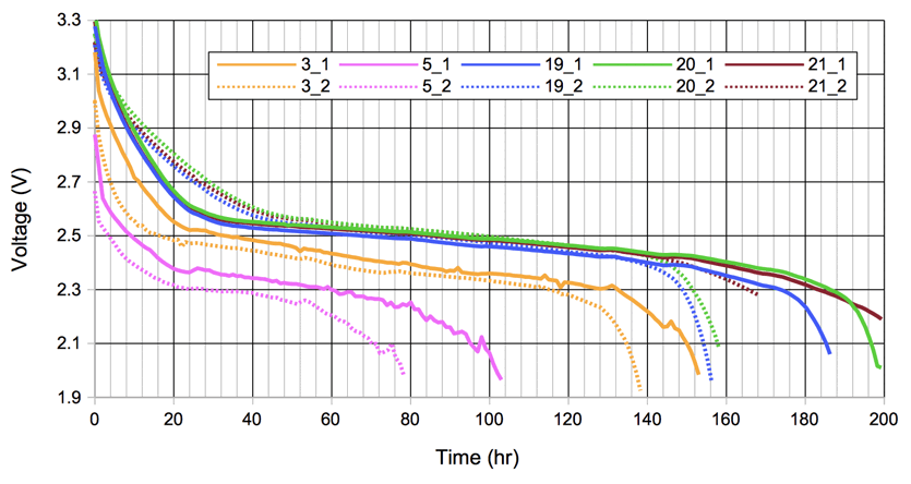
The above plot suggests that soldering directly to a ML621 manganese-lithium battery reduces both the operating voltage and the capacity of the battery. We connect all five batteries to our charger. Total current 900 μA. Poaching transmitters B206.193, C206.157, and C210.7 reception 100%, now joined by E210.25.
[05-NOV-18] Our five A3028T1-R have been charging for 60 hours. Total charge current is now 88 μA, down from 900 μA at start. Individual charge currents are T209.3 30 μA, T209.5 27 μA, T19 11 μA, T20 11 μA, T21 9 μA. The final charge current of a healthy ML621 is ≈10 μA. The current passes through two BAS116LPH4 diodes. Their combined voltage drop will be 1.1 V. With 4.2-V charging voltage, the voltage across the 1 kΩ resistor and battery combined will be 3.1 V. [We later discover that our charging voltage is only 4.1 V when the power supply meter shows 4.2 V, so charge voltage this time was 4.1 V.] We turn on all five transmitters and put them back in our cage. Poaching transmitters B206.193, C206.157, C210.7, and E210.25 100% reception, response to 20-MΩ sweep correct. Channel number, battery voltage (V) and noise (μV rms 2-160 Hz) are: 7 2.71 7.1 25 2.69 14.6 157 2.68 7.9 193 2.52 6.2.
[06-NOV-18] Poaching transmitters B206.193, C206.157, C210.7, and E210.25 100% reception, channel number, battery voltage (V) and noise (μV rms 2-160 Hz) are: 7 2.76 4.7 25 2.79 5.4 157 2.73 6.1 193 2.40 7.0.
[09-NOV-18] Poaching transmitters C206.157, C210.7, and E210.25 100% reception, response to 20-MΩ sweep correct. B206.193 has stopped after 24 days poaching. Diagnosis "Full Life". We have batch E210_27 consisting of eleven A3028E-AA. Frequency response E210_27 within ±0.5 dB. Switching noise ≤4 μV, total noise 2-160 Hz < 12 μV rms.
[12-NOV-18] Poaching transmitters C210.7, and E210.25, C206.157, 100% reception, VA = 2.72 V, 2.81 V, and 2.63 V. Our five A3028T1-R have discharged their batteries. T21 is still running, but battery voltage is 2.28 V. We connect 19-21 to our charger. The devices are initially active when we connect charging voltage, so we turn them off. Total charge current 650 μA.
[13-NOV-18] Three charging A30238T-R drawing 110 μA today. Poaching transmitters C210.7, and E210.25, C206.157, 100% reception, response to 20-MΩ sweep correct. We have an A3028U DC-160 Hz transmitter and a beaker of 1% saline. Start with Ag/AgCl electrode and its solder joint to a silver extension wire for C, and a silver wire on X. The tips of the stainless steel leads from C and X are out of the water, as is the transmitter body. We start recording M1542138183.ndf. We get this overview from 1000-1500 s. At time 1600 s we raise the solder joint in the C electrode above the water. We now have only a silver wire tip and an Ag/AgCl pellet with its attached silver wire within the saline. We get this from 1700-2200 s. From 2330-2445 s we are removing the Ag/AgCl pellet, scraping the silver wires, cutting off their tips, and replacing in saline, so we have two silver wires in water with no solder joints immersed. We get this from 3100-3600 s.
[15-NOV-18] Three charging A3028T1R drawing 15 μA today. But we note that the charging voltage is 4.1 V. We turn up to 4.2 V and see 45 μA. We check charge voltage with multimeter and get 4.21 V. Poaching transmitters C210.7, and E210.25, C206.157, 100% reception, response to 20-MΩ sweep correct.
[16-NOV-17] Three charging transmitter T19-21 consume 5 μA but we find that the charging voltage has dropped to 4.1 V. Increase to 4.2 V and see 35 μA. Remove from charger, turn on, place in beaker of water in faraday enclosure to discharge. Meanwhile, we have T209.19-22 encapsulated. Response to 20-MΩ sweep correct, noise ≤5 μV. We place on charger. Total input current 747 μA. Leave to charge for the weekend. Poaching transmitters C210.7, and E210.25, C206.157, 100% reception, battery voltages 2.70 V, 2.81 V, and 2.54 V respectively. We record from our A3028U 0-160 Hz transmitter with two silver wires in saline for 4500 s. We obtain this plot.
[19-NOV-18] Poaching transmitter C206.157 has stopped. This device sat on the shelf for four months, consuming 4.3 mAhr of its 48 mA-hr battery. It then ran for 820 hrs. Diagnosis "Full Life". C210.7 and E210.25 reception 100%, response to 20-MΩ sweep correct. Battery voltages 2.63 V and 2.81 V respectively.
[20-NOV-18] We have batch C210_41 consisting of 14 of A3028C-CC. Frequency response C210_41. Switching noise in 37°C water is ≤5 μV for all but 43, 45, and 56, which are 5-8 μV. Total noise is ≤10 μV rms in 2-80 Hz. Holding 43 and 56 for poaching. We have batch T209_19 consisting of four A3028T1-R. Final charge currents from 4.2 V supply through 1 kΩ were 5-6 μA. Frequency response T209_19. In 37°C water we have ID, reception (%), VBAT (V), and 1-40 Hz noise (uV rms): 19 100.00 3.22 2.7 20 100.00 3.27 3.0 21 100.00 3.28 2.8 22 100.00 3.30 3.0. So noise is ≤3 μV. Poaching transmitters C210.7, E210.25, C210.43, C210.53 100% reception.

[26-NOV-18] Devices T19-21, A3028T1R, now discharged, as shown above. Connect to 4.3 V to re-charge. Total current 800 μA. Poaching transmitters E210.25, C210.43, C210.53 100% reception, response to 20-MΩ sweep correct. C210.7 has stopped after 41 days, diagnosis "Full Life".
[27-NOV-18] Devices T19-21, A3028T1R, charging with 4.3 V, total current 170 μA. Poaching transmitters E210.25, C210.43, C210.56 ID, reception, VBAT, and rms noise uV: 25 99.85 2.77 4.6 43 100.00 2.70 11.3 56 97.46 2.68 10.2. We solder two teflon-insluted 125-μm diameter 316SS leads to U204.68 and two Ag/AgCl pellet electrodes to U204.69, both 512 SPS DC-160 Hz transitters. We fasten the transmitters outside a beaker of 1% saline, their leads passign over the rim of the beaker and down into the fluid. None of the leads are touching one another. Only the tips of the stainless steel leads are in the water. We place in our faraday enclosure and start continuous recording at 12 pm.
[28-NOV-18] Poaching transmitters E210.25, C210.43, C210.56 ID, reception 100%. Devices T19-21, A3028T1R, charging with 4.3 V, total current 60 μA. Remove from charger, each was taking 20 μA. The BAS116LPH4 drops 0.57 V at 20 μA, so batteries are getting 4.3−2×0.57 = 3.16 V through 1 kΩ. Remove U204.68 and 69 from faraday enclosure and turn off. Turn on T19-21 and place in faraday enclosure to monitor discharge. We analyze U204.68 and 69 twenty-two hour recording, extracting all events with power more than twice the average. We obtain thirteen events, all on channel 68. Nine are like the picture below.

Two are more vigorous oscillations that occur when we open the cage to remove the transmitters, see here. Two are glitches.
[30-NOV-18] We have batch A210.57 consisting of four A3028A-CCC. Gain versus frequency A210_57 within 0.2 dB. Switching noise in 45°C water is ≤1 μV. Total noise 2-160 Hz ≤10 μV after scrubbing solder joints and allowing ten minutes to settle. Poaching transmitters E210.25, C210.43, C210.53 frequency response here is correct.
[04-DEC-18] Poaching transmitters E210.25, C210.43, C210.56 reception 100% response to 20-MΩ sweep correct.
[07-DEC-18] Connect T19-21 A3028T1-R to recharger, current is 1 mA at first, 700 μA after an hour. Poaching transmitters E210.25, C210.43, C210.56 frequency response correct, reception 100%.
[10-DEC-18] Devices T19-21 A3028T1-R are drawing 35 μA from charger. Disconnect, turn on, and add to poaching jar. Poaching transmitters T19, T20, T21, E210.25, C210.43, C210.56 response to 20-MΩ sweep correct, reception 100%.
[11-DEC-18] Poaching transmitters T19, T20, T21, E210.25, C210.43, C210.56 100% reception. Receive 7 of A3028D-DDA returned from ION after three implantations and a total of six months implanted, but only 240 hours running, according to the records of the implanter. Examine D208.171. Silicone is intact but cloudy. Some components visible through silicone and epoxy on top side of circuit board. No breeches in silicone, antenna insulation intact, leads in good condition. Dissect. Silicone adhered well to epoxy. No sign of epoxy peeling away from components where the coating is thin. VB = 0.0 V. Disconnect, VB = 0.6 V. Connect external 2.6 V. Active current 146 &uA;. Leave for ten minutes, active current now 1.6 mA. Inactive 1.5 mA. Remove C2. Burning epoxy has a vinegar smell. Active current 145 μA. Inactive 1.4 μA. Response to 20-MΩ sweep correct. Diagnosis "Corroded Capacitor". Examine D208.173. As 171 including vinegar smell. Dissect. VB = 0.6 V. Disconnect, VB = 0.6 V. Connect external 2.6 V. Active 145 μA for a few minutes, then increasing to 2 mA. Inactive 2 mA. Remove C2 and C19, no change. Remove C20, active 146 μA, inactive 2.0 μA. Response to 20-MΩ sweep correct, but 173 is 2000 counts above 172. Diagnosis "Corroded Capacitor". Examine D208.163. As 171, including vinegar smell. Dissect. VB = 0.3 V. Disconnect, VB = 0.6 V. Connect externl 2.6 V. Inactive 40 μA. Clean and dry, inactive 75 μA. After a few minutes, inactive 115 μA, active 263 μA. Remove C2, active 152 μA. Response to 20-MΩ sweep correct on Y, 6 dB too low at all frequencies on X. Response to 50-Ω sweep correct on Y, 6 dB too low at 130 Hz on X. Active current now 147 μA. Examine D208.157. As 171, but do not notic vinegar smell. VB = 0.6 V. Disconnect 1.2 V. Active 15 mA. Remove C2, C19, C20 no change. Remove U3, inactive 3.5 μA. Short U3-4 to U3-6. Connect power wrong way around, current 150 mA. Connect the right way around, current 100 mA. Remove C1, C3 no change. Diagnosis "Corrosion Short".
[13-DEC-18] Poaching transmitters T19, T20, T21, E210.25, C210.43, C210.56 response to 20-MΩ sweep correct. Note poor reception from T19-21 in 60°C water in faraday enclosure when first removed from oven. After ten minutes, water has cooled to 45°C, reception is 100% from all.
[14-DEC-18] Dissect 208.179. Many bubbles in the epoxy surface over the battery. Cloudy patches under the silicone coating of the circuit. The edge of U5 is visible. VB = 1 V. Disconnect VB = 1.2 V. Connect external 2.6 V. Active 145 μA, reception 100%. Inactive 1.2 μA. Activate 145 μA. Reception 100%. Dissect D208.167. VB = 0.8 V. Disconnect VB = 1.1 V. Connect external 2.6 V. Active 300 &muA; Reception 100%. Increasing current over next minute to 750 μA. Inactive 600 μA. Remove C2. Inactive 1.3 μA. Active 153 μA. Dissect D208.161. VB = 0.5 V. Disconnect VB = 0.2 V. Inactive 2.6 μA. Active 150 μA. Reception 100%. Leave D208.167 (without C2), D208.179, D208.161 inactive and attached to 2.6 V through 1 kΩ. Return three hours later and D208.179 is consuming 1 mA when active, dropping back to 144 μA. Switch on and off a few times and get inactive 900 μA, active 1.05 mA. Remove C2. Resistance of C2 > 2 MΩ. Active 144 μA, inactive 2 μA, switching on and off ten times no aberration. Response to 20-MΩ sweep correct for 179, 161, and 167 correct. Of the seven returned, six show evidence of corrosion. Of these five recovered after removing one of the capacitors C2, C19, or C20. Diagnosis: corroded capacitor failure in at least 5 of 7. Given that these devices were implanted for roughly 150 days each, inactive for 90% of the time, the voltage-induced corrosion occurred only in the capacitors connected directly across the battery.
[14-DEC-18] Poaching transmitters T19, T20, T21 intermittent reception in air, E210.25, C210.43, C210.56 100% at 7 pm.
[18-DEC-18] Poaching transmitters T19, T20, and T21 have stopped. Connect to charger, they draw 1.0 mA together. Diagnosis "Full Life". After three hours we disconnect from charger and measure frequency response: T19 correct, T20 too high at 80 Hz, T21 oscillating at 40 Hz. Poaching transmitters E210.25, C210.56 response to 20-MΩ sweep correct, C210.43 response 6 dB too high at 40 Hz, 6 dB too low at 80 Hz for 20 MΩ source, but correct for 100-kΩ source. At 20°C in water we have ID, VBAT (V), Noise (uV): 25 2.69 14.9 43 2.48 6.5 56 2.15 8.7. We have batch D208.185 consisting of four A3028D-DDA. Scrup solder joints on pins and place in 40°C water. Noise is <12 μV, switching noise <3 μV. Frequency response D208_185 within ±0.3 dB. We add D208.189 and D208.193 to poach at 60°C inactive, to test inactive implant corrosion resistance.
[20-DEC-18] We have batch P207.73 consisting of eleven A3028P1-AA. Frequency response P207_73 within ±0.45 dB. Noise in 1-40 Hz <4 μV, switching noise <1 μV. Hold back P207.73 for poaching. Poaching transmitters E210.25, C210.43, C210.56, D208.189, and D208.193 reception 100%. Response to 20-MΩ sweep correct for all, except C210.43 gain 6 dB too high at 40 Hz and 6 dB too high at 80 Hz, and for twenty seconds sustains its own oscillations at 40 Hz with leads open circuit. Similar problems with 100-kΩ source and 50-Ω source. Gain is too great at 40 Hz.
[21-DEC-18] Poaching transmitter C210.56 has stopped. C210.43 reception 100%, VA = 2.17 V, 20-MΩ sweep 6 dB too high at 40 Hz, 6 dB too low at 80 Hz. E210.25 100%, sweep correct. D208.189 and D208.193 100%, sweep correct. Recharging T19-T21 together draw 40 μA from 4.3V through individual 1-kΩ resistors. Turn them on. Reception 100%, sweep correct for all three VA = 3.3-3.4 V. These have 0.3-80 Hz filters but only 128 SPS so we are able to see aliasing clearly with frequencies 50-70 Hz. Add P207.73 to poach. Dissect C210.56. VB = 0.5 V. Encapsulation in perfect condition. Good adhesion of silicone. Disconnect, VB = 0.4 V. Connect external 2.6 V. Active 52 μA, reception 100%, inactive 1.3 μA. At 60°C its current consumption would be 10% higher because of the effect of temperature upon the circuit and 5% higher because the battery voltage increases, so a total of 15% hihgher makes60 μA for 800 hr. This device ran for 744 hours at 60°C. It's battery voltage on 12DEC18 was 2.15 V. After an hour, current consumption at room temperature is 51 μA. Diagnosis "Unidentified Drain".
[24-DEC-18] Poaching transmitter C210.43 response to 20-MΩ sweep correct when freshly removed from hot water is correct. As it cools, oscillations at 40 Hz develope, replace in hot water, oscillations stop after thirty seconds. Reception 100%, VA = 2.50 V. Transmitters T19, T20, T21 in hot water reception 100%, noise ≤10 μV, VB ≈2.6 V. When we allow to cool to room temperature in air, T21 starts oscillating at around 40 Hz. We return to hot water and oscillations stop in thirty seconds. We place T19-T20 in the oven to bake for half an hour. Now all three provide correct response to 20-MΩ sweep, but after five minutes at room temperature, T21 starts oscillating at around 60 Hz. Place in the oven for another half-hour. Upon removel, all three provide correct response to 20-MΩ. Drop in 20°C water. After five minutes, no oscillations. Remove and find sweep response correct. Return to poach. P207.73, E210.25, D208.189 and D208.193 reception 100%, response to 20-MΩ sweep correct. Switch off D208.189 and D208.193.
[26-DEC-18] Poaching transmitters reception 100% except C210.43, which has stopped. Diagnosis "Full Life". For 1-s intervals ID, VA (V), Noise (uV rms 1-40 Hz): 19 2.48 4.2 20 2.51 14.1 21 2.52 3.3 25 2.73 8.3 73 3.02 3.4 189 2.70 6.6 190 2.72 6.5 193 2.69 15.3 194 2.67 12.8.
[27-DEC-18] Poaching transmitters immediately after removal from oven, 1-s intervals ID, VA (V), Noise (uV rms 1-40 Hz): 19 2.42 3.2 20 2.46 4.1 21 2.46 4.1 25 2.77 3.6 73 3.02 2.9. Turn on D208.189 and D208.193, reception 100%, response to 20-MΩ sweep correct. Remove each of the remaining one by one from water. T19, T20 sweep correct. T21 sweep correct for a few seconds, then 2-Hz square wave starts up. P207.73 and E210.25 sweep correct.
[28-DEC-18] Poaching transmitters T19 and T20 have stopped, but T21 still running with VA = 2.19 V. Diagnosis "Full Life". Remove, connect all three to 4.3 V with their own 1-kΩ resistor and see total current 0.9 mA. For remaining devices reception is 100% and in 1-s intervals we have ID, VA (V), Noise (uV rms 1-40 Hz): 25 2.73 8.3 73 3.02 3.2 189 2.77 17.2 190 2.78 15.0 193 2.74 5.3 194 2.74 7.1.
[31-DEC-18] Poaching transmitters P207.73, E210.25, D208.189, D208.193 response to 20-MΩ sweep correct, reception 100%. Charging current for T19, T20, T21 is 38 μA. Sweep response correct for T19 and T20, but T21 has unstable baseline. Put in oven to dry for an hour, then add to poaching water in inactive state, like D208.189 and D208.193.
[08-JAN-19] Poaching transmitters P207.73, E210.25, D208.189, D208.193, T19, T20, T21 reception 100%. T19 generating 1-Hz square wave, no response to 20-MΩ sweep. T20 and T21 rumble of around 100 μV, correct response to 20-MΩ sweep. P207.73, E210.25, D208.189, D208.193 correct response to 20-MΩ sweep.
[09-JAN-19] We have batch K207.55 consisting of 12 of A3027K-AA 0.3-40 Hz, 128 SPS, 1.3 ml. Frequency response K207_55 within ±0.7 dB. Noise 1-40 Hzz in 37°C water <7 μV, switching noise ≤ 5 μV except for K207.65 and K207.68, which have 1-40 Hz noise 8 μV and switching noise 6 μV, see spectrum. All are okay to ship, but hold back these last two for poaching.
[10-JAN-19] Add K207.65 and K207.68 to poach. ID, VA (V), and 1-40 Hz noise (uV): 25 2.72 9.4 65 2.76 6.3 68 2.87 3.8 73 3.18 2.9 189 2.76 9.0 190 2.76 26.8 193 2.72 8.0 194 2.72 20.2. T19-21 turn on and transmit 100%.
[11-JAN-19] Poaching transmitters 100% reception.
[14-JAN-19] Poaching transmitters 100% reception except for P207.73, which has stopped. K207.65 and K207.68 response to 20-MΩ sweep correct.
[15-JAN-19] Add P207.105 to 60°C poach. This device had its red lead replaced after epoxy encapsulation, so we won't expect its amplifier to resist corrosion, but we can test it for battery drain. Poaching transmitters K207.65, K207.68, E210.25, D208.193, P207.105 100% reception and response to 20-MΩ sweep correct. D208.189, T19 100% reception and response to 100-kΩ sweep correct. T21 100% reception, response to 100-kΩ sweep a 1-Hz full-scale oscillation plus response to sweep. T20 won't turn on. Connect to 4.3V through 1 kΩ see 300 μA flow in. After twenty minutes, 180 μA. Now get 100% reception and response to 100-kΩ sweep is a 1-Hz square wave. Re-connect to charger. Dissect P207.73. VB = 0.5 V. Disconnect, VB = 0.6 V. Connect external 2.7 V. Inactive 0.8 μA. Active 31 μA.
We begin another search for slow artifacts with our two DC-160 Hz single-channel mouse transmitters. We equip U204.68 with two bare wire electrodes fastened to a simulated animal skull made of dental cement with 00-80 screws. We place in a covered petri dish filled with 1% saline. We equip U204.69 with two crimp electrodes. One consists of 3 mm of steel tube crushed around the bare spring. The other consists of 3 mm of steel tube crushed around the spring and a 125-μm steel wire.

We place in faraday enclosure and start recording. We are looking for artifacts like the one shown below, recorded with an A3028U-AA two-channel DC-160 Hz device.
[18-JAN-19] We have batch P207.87 consisting of eleven A3028P1-AA. Frequency response P207_87, except omit P207.114 because it's bandwidth is 0.3-80 Hz, when it should be 0.3-40 Hz. Noise 1-40 Hz <4 μV, switching noise <1 μV. Keeping P207.114 for poaching, inactive test starting today. Poaching transmitters K207.65, K207.68, E210.25, P207.105, D208.193 100% reception and response to 20-MΩ sweep correct. D208.189 100% reception and response to 100-kΩ sweep correct. T19 and T21 100% reception. T20 we have re-charged. Charge current now 2.5 μA. Response to 20-MΩ sweep correct. Turn on and place in faraday enclosure at 13:40 18-JAN-19. We return to our DC transmitters and produce a write-up here.
[22-JAN-19] Poaching transmitters K207.65, K207.68, E210.25, P207.105, D208.189, D208.193, P207.114 100% reception and response to 100-kΩ sweep correct. T19 and T21 100% reception. We have batch B205.21 consisting of ten of A3028B-DD, but we note that they don't have their pins soldered on yet. Frequency response B205_21 within ±0.2 dB. Noise 2-160 Hz in 40°C water ≤8.0 μV except B205.28 is 14 μV, switching noise ≤3 μV.
[23-JAN-19] Poaching transmitters K207.65, K207.68, E210.25, P207.105 100% reception. Don't turn on the inactive test devices.
[24-JAN-19] We have batch D208_195 consisting of ten A3028D-DDA. Frequency response D208_195 within ±0.3 dB. Switching noise in 37°C water <2 μV, total noise 1-160 Hz after scrubbing pins ≤11 μV. Poaching transmitters K207.65, K207.68, E210.25, P207.105 100% reception. Don't turn on the inactive test devices.
[25-JAN-19] T20 ran its battery down in 122 hours. Recharging now with 200 μA now. Poaching transmitters K207.65, K207.68, E210.25, P207.114, D208.189, D208.193 100% reception, response to 100-kΩ sweep correct. P207.105 response to 100-kΩ sweep 3 dB too low at 40 Hz, reception 100%, generates square wave in water. Recall that this device had its X-lead replaced by burning epoxy, so we expect early failure of its amplifier. T19 and T21 reception 100%, both generating 1-Hz square wave in water.
[29-JAN-19] Poaching transmitters K207.65, K207.68, E210.25, P207.114, D208.189, D208.193, P207.105 100% reception, response to 100-kΩ sweep correct. Note that P207.105 has recovered since previous test. T19 and T21 reception 100%, both generating 1-Hz square wave in water. T20 is drawing 8 μA from charger. Charging voltage 4.37 V. Turn on and place in water in faraday enclosure to exhaust battery.
[31-JAN-19] Poaching transmitters T19, T21, K207.65, K207.68, E210.25, P207.105, P207.114, D208.189, D208.193 100% reception.
[01-FEB-19] We have two A3028D-DDA, D208.219 and D208.221. Frequency response D208_219 within ±0.7 dB. Switching noise in 37°C water is <2 μV, 2-160 Hz noise <12 μV after much scrubbing of the solder joints. Poaching transmitter E210.25 has stopped. K207.65, K207.68, P207.114, D208.189, D208.193, P207.105 100% reception and correct response to 100-kΩ sweep. Dissect E210.25. VB = 0.6 V. Disconnect, VB = 2.7 V. Connect external 2.7 V. Inactive 3.1 mA. Active 3.2 mA, 100% reception. Heat up C5 and C2 with 370°C iron. Active 78 μA. Diagnosis "Corroded Capacitor". We have two A3028GV1 circuit boards from B78082. When programmed as A3028B they consume 100 μA, higher than the typical 78 μA. We disable the logic chip functions and current is 50 μ. We remove logic chip and tie U9-4 to U9-3 to disable the VCO. Active current 300 μA for both. We connect U7-1 to U7-10 to send U7 to sleep. But current is still 300 μA in both, and R4 is dropping 0.3 V. We connect U7-6,7,8 to U10-9 but still get 300 μA. Remove U7 and get 10 μA from both, which is about right for what we have left on the board.
[04-FEB-19] Poaching transmitters T19, T21, K207.65, K207.68, P207.105, P207.114, D208.189, D208.193 100% reception and correct response to 100-kΩ sweep. T20 has stopped. It ran for 130 hours. Attach to 4.4 V through 1.0 kΩ and it draws 600 μA at first, then 150 μA after twenty minutes.
[05-FEB-19] We receive four A3028T1-R, T209.1, 2, 4, and 10. These were charged and shipped in September and October. T209.1 and T209.10 turn on with VA = 2.19 V and 2.23 V respectively. T209.2 and T209.4 won't turn on. Connect to 4.4-V 1-kΩ charger. Charge currents 170, 40, 270, and 140 μA respectively. We remove No2 and find it turns on for a few minutes. Re-connect to charger and see only 40 μA current. Leave them all connected, along with T20, which now draws 50 μA. Poaching transmitters T19, T21, K207.65, K207.68, P207.105, P207.114, D208.189, D208.193, 100% reception.
We have another A3028GV1 from B78082 with active current consumption 100 μA when it should be 80 μA. Remove U9, the VCO, and current drops to 73 μA. Remove U7 and current is 66 μA. Remove U6, 62 μA. Remove U5 61 μA. Reprogram U8 to eliminate state machines and ring oscillator, 39 μA. Remove U10, 34 μA. Remove U8, 2.5 μA. Turn off with magnet, 1.4 μA.
We have batch A3028S_67 consisting of fifteen of A3028S2Z-AA before encapsulation. These devices have bandwidth DC-80 Hz, 256 SPS, and dynamic range ±100 mV. We apply 200 mVpp through 50-Ω at 10 Hz to the input of S210.74 and see 14702 cnt rms. The amplifier gain is 4.8 μV/cnt. We apply 345 mVpp through 20 MΩ to the input at 10-Hz. We see 7485 cnt rms on the transmitted signal, or 102 mV pp. The input resistance is 8.4 MΩ. We apply a 0.1-Hz, 200 mVpp square wave through 50 Ω and the output stable after the steps to ±5 μV for three seconds, suggesting a time constant of at least three hours. We proceed to check the response of all circuits with a 350-mVpp, 20-MΩ, 1-Hz square wave, looking at the bounce after the steps to confirm frequency response.

Considering the response above, assuming the nominal 10-MΩ input resistance, we expect 115 mVpp on X. The nominal amplifier gain is 10.0, so 1.15 Vpp appears on the ADC input. Our battery voltage was 2.55 V, so we expect 29 k-cnt-pp. We observe 22 k-cnt-pp.
[07-FEB-19] Device T209.2 failed to re-charge: after one day its recharge current was still the same 40 μA, we place in enclosure and it runs down its battery in a few hours. Devices T209.1, 4, and 10 together consume 50 μA from the charger after two days. We place in 37°C water and get VA (V) and 2-40 Hz noise (μV rms): 3.39 5.1 3.19 6.5 3.39 2.7. Response to 20-MΩ sweep correct. Ready to return to customer. Poaching transmitters T19, T21, K207.65, K207.68, P207.105, P207.114, D208.189, D208.193 100% reception.
[11-FEB-19] Poaching transmitters K207.65, K207.68, P207.105 100% reception. Do not turn on the inactive devices.
[12-FEB-19] We observe yellow and brown staining around the BR1225 batteries we soldered to A3028PV1 circuits for A3028S2Z and subsequently encapsulated. The circular plastic seal between the terminals is deformed in these cases. We reproduce the effect on fresh batteries. With the help of acid flux and care taken to avoid touching the battery near the seal, we load three batteries onto three circuits and program then as A3028P5, current consumption 250 μA, P177, P178, P179. There is no sign of damage to the seals on these devices, but 179 has a stain between the seal and the wire joint that we cannot remove with water washing. Of our batch of 15 A3028S2Z we find that seven have damaged seals but batteries still deliver ≈2.8 V, one has a damaged seal and its battery is drained, and seven have no sign of damage on their seals and deliver ≈2.8 V.

We select four devices with damaged seals that still run: S210.70, 72, 73, and 78. We re-program as S5 and place them in an enclosure to run down. Of the seven that show no sign of seal failure, we take S210.68 and re-program as S5 and place in enclosure to run down. We remove the battery from S210.67 and find quiescent current 51 μA. We clean up the epoxy and solder a new battery to the circuit board.

Poaching transmitters T19, T21, K207.65, P207.105, P207.114, D208.189, D208.193, 100% reception. K207.68 has stopped and will not turn on. K207.65, P207.114, D208.189, D208.193 correct response to 100-kΩ sweep. Don't test the others. Dissect K207.68. VB = 1.0 V. Disconnect 1.6 V. Connect external 2.7 V. Inactive 1.6 μA. Active 36 μA. Reception 100%. Diagnosis "Unidentified Drain". Device T209.2, which failed to re-charge, we dissect. We remove the battery and find active current 32 μA.

The four devices with visible battery damage expired within 64 hours. The remainder are still running well. The nominal battery life at 250 μA is 190 hrs.
[18-FEB-19] Poaching transmitter K207.65, D208.189, D208.193 100% reception, response to 100-kΩ sweep correct. T19, T21 100% reception. P207.114 100% reception but generates its own 60-Hz oscillation even in water. P207.105 has stopped. Place T20 back in enclosure after five days charging.
[19-FEB-19] Of our eight A3028S5Z circuits, only three are still running. The four with visible battery discharge all failed within 65 hr. The one with a stain between the seal and the wire joint failed after 156 hr. The other three are running after 170 hr. We see the battery voltage being affected by temperature, which varies from 10-20°C in our office.

Looking at the figure above, the capacity of the batteries in our test, with 250-μA load and 12°C average temperature, is around 42 mA-hr, instead of the usual 48 mA-hr we assume for implanted BR1225, making the nominal operating life 168 hr.
We have batch T209_23 consisting of four A3028T1-R-AA. In 37°C water we have ID, VB (V), and noise 2-40 Hz (uV rms) is: 23 2.64 3.0 24 2.63 3.7 25 2.63 4.5 26 2.64 3.9. No sign of switching noise <0.8 μV. Frequency respose T209_23 correct. Connect to 4.4-V 1-kΩ charger and see total current 1 mA evently distributed. We have batch B211_1 consisting of eleven A3028B-AA. Frequency response B211_1 within ±0.4 dB. Noise 2-160 Hz in 37°C water is ≤11 μV, switching noise ≤4 μV.
Dissect P207.5. Yellow corrosion around base of red lead, where we re-soldered. Remove silicone and stain of corrosion lies in a trail from the joint to the negative battery wire which appears to have a spot of bare metal. VB = 0 V. Disconnect, VB = 0V. Connect external 2.7 V, Active 33 μA, inactive 0.8 μA. Diagnosis "Unidentified Drain". Poaching transmitter K207.65, D208.189, D208.193 100% reception. K207.65 response to 100-kΩ sweep correct. T19, T21 100% reception. P207.114 100% reception but generates oscillation.
[20-FEB-19] Poaching transmitter K207.65 100% reception but VA = 2.18 V. Batch T209_23 four A3028T1-R-AA still charging, combined current 55 μA.
[20-FEB-19] Batch T209_23 four A3028T1-R-AA still charging, combined current 25 μA. Remove from charger, turn on and place in 20°C water, get ID, VBAT (V), and noise 2-40 Hz (μV rms): 23 3.43 2.8 24 3.49 2.7 25 3.47 2.9 26 3.46 2.9. Ship T209.23. Keep the other three running in water in faraday enclosure. Poaching transmitter K207.65 has stopped. Inactive poaching transmitters D208.189, D208.193, P207.114, T19, and T21 100% reception. Dissect K207.65. Silicon and epoxy inaffected by 42-day poach. VB = 0.8 V. Disconnect, VB = 0.8 V. Connect external 2.7 V. Active 38 μA, inactive 4.0 μA. Increase voltage to 4.1 V, inactive current 15 μA. Active current 48 μA. Reception 100%. Drop voltage to 2.7 V and inactive current is now 1.6 μA. Diagnosis "Corrosion Short". We have 5 of A3028S2Z-AA upon which we have replaced the batteries because of discharge visible through the epoxy. We have coated them in silicone. We turn on and place in warm water. We get ID, VBAT (V), and noise 2-80 Hz (μV rms): 67 2.97 3.7 70 2.73 4.3 72 2.75 3.1 73 2.72 5.0 78 2.70 3.8. The No67 battery voltage 2.97 V is sustained. We leave to soak in water.
[25-FEB-19] We have batch L210_85 consisting of 12 of A3028L-DDA. Of thse, one, L210.89, does not turn on. Frequency response L210_85 within ±0.7 dB. Noise in 37°C water 2-320 Hz ≤14 μV, switcing noise <1 μV.
[26-FEB-19] Dissect L210.89. VB = 0.3V. Disconnect VB = 2.2 V. Connect external 2.7 V. Active 14.83 mA, inactive 14.82 mA. Lever circuit board off batter but break off most of the parts on the top side of the board. There is a cavity over the logic chip. We cannot determine the source of the high current drain.
[28-FEB-19] Inactive poaching transmitters D208.189, D208.193, P207.114, T19, and T21 100% reception.
[01-MAR-19] We have batch S210_67 consisting of 15 of A3028S2Z-AA with lead lengths 35 mm or 100 mm. We apply 0.25 Hz, 160-mVpp 20-MΩ sweep. We see 12.4 kcnt-pp amplitude on the input. With 10-MΩ input impedance we expect the voltage on the transmitter input to be 53 mVpp. Scale is is 4.3 μV/cnt, dynamic range 280 mV. Assuming battery voltage 2.6 V, amplifier gain appears to be 9.2 at 0.25 Hz. Gain versus frequency S210_67 within ±0.9 dB. Input noise 2-80 Hz in 37°C water is ≤ 50 μV rms with switching noise ≤34 μV. S210.68 has sample rate 2048 SPS, so must reject. S210.73 has some cloudy patches in the silicone over the battery. S210.78 has leads that are only 37 mm long.

[05-MAR-19] Inactive poaching transmitters D208.189, D208.193, P207.114, and T21 100% reception. Gain versus frequency for D208.189 and D208.193 correct on all channels for 100-kΩ sweep. P207.114 and T21 generating their own square waves. T19 won't turn on. We add S210.67 and S210.78, both A3028S2Z, and S210.68 an A3028S5, to the poach for active test. T20 ran for 120 hours during its most recent discharge. We dissect and find active consumption is 29 μA with 2.5-V supply, inactive is 0.8 μA. Dissect T19. Inactive current 0.9 μA, active 6.0 mA. Increase supply to 4.2 V, active 2.0 mA. Drop back to 2.5 V, 1.3 mA. Diagnosis "Corroded Capacitor".
We complete discharge of three BR1225 soldered to A3028S5 circuit board, average current consumption 250 μA, and obtain this plot of battery voltage versus time. Operating live is 190 hrs, or 48 mA-hr. Nominal capacity 48 mA-hr. We complete discharge of three ML621 encapsulated in A3028T1-R-AA, average current consumption 32 μA, and obtain this plot of battery voltage versus time. Operating life is 230 hrs, or 7.4 mA-hr. Nominal capacity 5 mA-hr. Connect the three A3028T1R to charger 4.4 V in series with 1 kΩ. Current is 700 μA.
[07-MAR-19] Active poaching transmitters S210.67, S210.68, and S210.78 100% reception. Inactive poaching transmitters D208.189, D208.193, P207.114, and T21 100% reception. T21 and P207.114 producing a variety of 0.5-Hz oscillations.
[08-MAR-19] Three A3028T1R charging with current 43 μA after three days connected. Disconnect, turn on, place in enclosure and start another discharge.
[11-MAR-19] Active poaching transmitters S210.67, S210.68, and S210.78 100% reception and response to 100-kΩ sweep correct. Inactive poaching transmitters D208.189, D208.193, P207.114, and T21 100% reception.
[12-MAR-19] Active poaching transmitters S210.67, S210.68, and S210.78 100% reception.
[14-MAR-19] Active poaching transmitters S210.67, S210.68, and S210.78 100% reception. Battery voltages 2.81 V, 2.00 V, and 2.79 V respectively. After a few minutes cooling down, S210.68 stops. Noise in 67 and 78 is roughly 35 μV rms, accounting for the gain of ×10 for these A3028S2Z devices.
[15-MAR-19] Active poaching transmitters S210.67 and S210.78 100% reception. Battery voltages 2.79 V and 2.78 V respectively.
[18-MAR-19] A transmitter in quality control, B210.165, has C15 not soldered at one end. The Y amplifier produces 2.6 Vpp 180-Hz oscillation. We see 300 μV amplitude 180 Hz in the spectrum of the X input. We fix C15 and the noise on X stops. Active poaching transmitter S210.67 has stopped, and S210.78 reception is 100%, but it generates a half-scale 100-Hz oscillation.
[19-MAR-19] We have batch L210_117 consisting of fifteen A3028L-DDA. Frequency response L210_117 within ±1 dB for all thirty channels. In 37°C water, after scrubbing leads, noise 2-320 Hz ≤12 μV with switching noise <1 μV. With 20 channels at 1024 SPS we have 30 KSPS. We have two antennas and find that average reception is 70%. We remove one antenna and average reception is 69%. Loss is dominated by collisions, and collisions occur simultaneously at both antennas. Dissect S210.67. Silicone intact, but see pronounced white stains at two points around the rim of the positive battery terminal. VB = 1.9 V. Disconnect battery, connect exterior 2.6 V. Current is 2 mA at first, then drops to 50 μA after a ten seconds. Jumps up above 1.5 mA for a few seconds, returns to 49 μA. Does this again. Diagnosis "Corroded Capacitor".
Active poaching transmitter S210.78 100% reception, ≈100 Hz oscillation. Inactive poaching devices T21, P207.114 100% reception 1-Hz full-scale oscillation. Inactive poaching D208.193 100% reception and 100-kΩ sweep correct. Inactive poaching D208.189 100% and 100-kΩ sweep correct on channel 189, but 10 dB too low at 100 Hz on 190.
[22-MAR-19] Active poaching transm itter S210.78 100% reception. At first generates 125 Hz oscillation, but then settles down to quiet, and response to 100-kΩ sweep correct. Our three A3028T1-R have been charging for three days, total current is now 25 μA. We turn them on and put them in water in a faraday enclosure.
[25-MAR-19] Active poaching transm itter S210.78 100% reception generates 125 Hz oscillation. Inactive poaching devices T21, P207.114, D208.189, and D208.193 100% reception.
[26-MAR-19] We have batch B210_153 consisting of fourteen A3028B-CC. Frequency response B210_153 within ±0.5 dB. Noise 2-160 Hz is ≤10 μV rms and switching noise <3 μV except No167, which has total noise 15 μV rms and switching noise 5 μV. We set this one aside. We also have No155 noted as being left on for some time during encapsulation, so we set this one aside also. Active poaching transm itter S210.78 100% reception generates 125 Hz oscillation.
[28-MAR-19] Active poaching transmitter S210.78 100% reception generates 125 Hz oscillation.
[29-MAR-19] Active transmitter S210.78 100% reception, no oscillation, VA = 1.9 V. Inactive poaching devices T21, P207.114, D208.189, and D208.193 100% reception.
[01-APR-19] Active transmitter S210.78 100% reception, no oscillation, VA = 1.9 V. Inactive poaching devices T21, P207.114, D208.189, and D208.193 100% reception. Yesterday we find our three discharging A3028T1-R devices have exhausted their batteries after 205 hrs. We connect to recharger and see a total of 1.5 mA. Today we see 0.5 mA. Three discharge curves are here.
[09-APR-19] Active transmitter S210.78 100% reception, no oscillation, VA = 2.7 V, response to 100-kΩ sweep correct. Inactive poaching devices P207.114, D208.189, and D208.193 100% reception. P207.114 produces square wave, D208.189, and D208.193 correct response to 100-kΩ sweep. Inactive poaching device T21 won't turn on. Start recharging, but input current only 45 μA.
[12-APR-19] Active transmitter S210.78 100% reception.
[15-APR-19] Active transmitter S210.78 has turned off. Diagnosis "Full Life". Inactive poaching devices P207.114, D208.189, and D208.193 100% reception.
[16-APR-19] Begin active poach at 60°C of A3028B B210.155 and B210.167. B210.155 we did not ship because we left it on for between one and four days by mistake. B210.167 we did not ship because it was noisy. We have B211.9 back from customer after three months on the shelf. Dissect VB = 0.1 V. Disconnect VB = 0.2 V. Apply external 2.6 V. Active 80 μA, inactive 1.3 μA. Diagnosis: "Full Life", was left on by accident.
[23-APR-19] Poaching transmitters B210.155, B210.167, D208.189, D208.193, P207.114 100% reception. Response to 100-kΩ sweep correct for D208.189 X but gain 10 dB too low on Y, correct for D208.193 X, 6 dB too high at 130 Hz for Y, correct for B210.155 and B210.167. P207.114 gives 1-Hz square wave.
[29-APR-19] We have batch C210.169 consisting of seven A3028C-CC. Frequency response C210_169 within ±0.8 dB. Noise 2-80 Hz is ≤8 μV, switching noise <4 μV.
[30-APR-19] Poaching transmitters B210.155, B210.167 100% reception.
[01-MAY-19] Active poaching transmitters B210.155, B210.167 100% reception, response to 100-kΩ sweep correct. Inactive poaching transmitter D208.189 100% reception, 100-kΩ sweep response 10 dB too low at 100 Hz on both channels. Inactive poaching transmitter D208.193 100% reception, 100-kΩ sweep response 10 dB too high at 100 Hz on one channel. Inactive poaching transmitter P207.114 won't turn on.
[03-MAY-19] We have batch A210.179 consisting of six A3028A-CCC transmitters. Gain versus frequenvy A210_179 within ±0.3 dB. Noise 2-160 Hz ≤10 μV rms. Switching noise ≤3 μV.
[06-MAY-19] Active poaching transmitter B210.167 100% reception, but B210.155 has stopped.
[06-MAY-19] Active poaching transmitter B210.167 100% reception, response to 100-kΩ sweep correct. Inactive poaching transmitter D208.189 100% reception, 100-kΩ sweep response 10 dB too low at 100 Hz on both channels. Same with 50-Ω sweep. Inactive poaching transmitter D208.193 100% reception, 100-kΩ sweep response 10 dB too high at 100 Hz on one channel, correct on the other. Same with 50-Ω sweep. Dissect B210.155. VB = 0.4 V. Disconnect VB = 0.4 V. Connect external 2.6 V. Inactive 1.4 μA, active 87 μA, reception 100%, response to 100-kΩ sweep correct. Expected life with 87 μA is 23 days, this transmitter ran for several days before test began, so diagnosis is "Full Life". Dissect P207.114. Remove battery and connect external 2.6 V. Inactive 1.0 μA. Active 33 μA for a minute, then jumps to 400 μA. Diagnosis "Corroded Capacitor".
[10-MAY-19] Active poaching transmitter B210.167 100% reception, response to 20-MΩ sweep correct.
[13-MAY-19] Active poaching transmitter B210.167 has stopped. Diagnosis "Full Life".
[14-MAY-19] We have four bare A3028GV1 circuit boards that show current consumption roughly 30 μA higher than usual.

We remove all components except logic power supplies and logic chip from one circuit board. The current consumption of what is left is 27 μA, which is 13 μA higher than the typical current consumption of the logic chip (11 μA) plus the typical current consumption of the magnetic switch (2 μA) and flip-flop (0.5 μA).
[21-MAY-19] We have three A3028GV1 with roughly 10 μA excessive current consumption. We program them as A3028K, 128 SPS, nominal current 35 μA. They are now K209, K210, and K211, with current consumption 52.5 μA, 51.4 μA, and 48.6 μA respectively. We solder CR1220, 30-mAhr batteries to their programming extensions and place them in a Faraday enclosure. If their current consumptions remain constant, we expect their operating lives to be 570, 580, and 620 hrs respectively.
[24-MAY-19] We have batch B205_34 consisting of 11 of A3028B-DD. Frequency response B205_34 within 0.4 dB. Switching noise in 38°C water ≤4 μV amplitude, total noise 2-160 Hz ≤12 μV except for B205.37, which shows persistent rumble 2-5 Hz of 40-100 μV, despite brushing and instpecting electrode pins.
[28-MAY-19] We have batch B211_13 consisting of 12 of A3028B-AA with 55-mm leads tipped with bare-wire electrodes. Frequency response B211_13 within ±0.4 dB. Total noise 2-160 Hz in 37°C water ≤8 μV, switching noise ≤4 μV. We have B205.59 with 90-mm leads terminated with D-pins. Its total noise before scrubbing pins is 100 μV rms, after scrubbing 20 μV rms, and its switching noise is 5 μV. We set this one aside to poach.
Inactive poaching transmitters D208.189 and D208.193 100% reception. Inspect encapsulation. Original ripples in silicone remain unchanged. Label print is fading. No sign of rust. Can still see a few components through the silicone and thin layer of epoxy. Both transmitters generating 1-Hz square waves on both channels when open-circuit in air. Add to active poach B205.59 and B211.25. The latter's current consumption during quality control was 84 μA.
[31-MAY-19] Active poaching transmitters B205.59 and B211.25 100% reception.
[04-JUN-19] Active poaching transmitters B205.59 and B211.25 100% reception, response to 100-kΩ sweep correct. Inactive poaching transmitters D208.189 and D208.193 100% reception.
[07-JUN-19] Active poaching transmitters B205.59 and B211.25 100% reception, response to 100-kΩ sweep correct. Inactive poaching transmitters D208.189 and D208.193 100% reception.
[11-JUN-19] Active poaching transmitters B205.59 and B211.25 100% reception. The faulty A3028GV1 circuits with current consumption roughly 10 μA too high at time of quality assurance take 700 hours to run down a 30 mA-hr battery, see below. If their current consumptions had remained constant, and the capacit of the battery were 30 mAhr, we would expect their operating lives to be 570, 580, and 620 hrs respectively.

[19-JUN-19] We have batch C207_116 consisting of twelve of C3028C-AA. Frequency response C207_116 ±0.8 dB. Gain is higher at 2 Hz than usual, but all are the same, and all are within ±2 dB of nominal. Noise in 37°C water is ≤6 μV 2-80 Hz, switching noise ≤3 μV. Active poaching transmitters B205.59 and B211.25 100% reception.
[21-JUN-19] Active poaching transmitter B211.25 100% reception and correct response to 100-kΩ sweep, B205.59 has stopped. Diagnosis "Full Life". Inactive poaching transmitters D208.189 and D208.193 100% reception.
[24-JUN-19] Active poaching transmitter B211.25 has stopped. Diagnosis "Full Life". Inactive poaching transmitters D208.189 and D208.193 100% reception.
[22-JUL-19] We have batch E200_125 consisting of 12 of A3028E-FB. Frequency response E200_125.gif within ±0.4 dB. Noise 2-160 Hz ≤12 μV, switching noise in 37°C water ≤4 μV. Inactive poaching transmitters D208.189 and D208.193 100% reception. Add E200.125 and E200.126 to active poach.
[23-JUL-19] Inactive poaching transmitters D208.189 and D208.193 100% reception. Active poaching transmitters E200.125 and E200.126 100% reception, response to 20-MΩ sweep correct.
[26-JUL-19] Inactive poaching transmitters D208.189 and D208.193 100% reception. Active poaching transmitters E200.125 and E200.126 100% reception, response to 20-MΩ sweep correct. We have batch C207_130 consisting of nine of A3028C-AA. Frequency response C207_130 within ±0.9 db. Noise 1-80 Hz ≤5 μV except No13710 μV. Switching noise <4 μV.
[05-AUG-19] Inactive poaching transmitters D208.189 and D208.193 100% reception. Active poaching transmitters E200.125 and E200.126 100% reception, response to 20-MΩ sweep correct.
[06-AUG-19] We have batch E212_1 consisting of eleven of A3028E-AA. Frequency response E212_1 within ±0.8 dB. Switching noise in 37°C water ≤2 μV. Total noise 1-160 Hz 5-9 μV rms.
[09-AUG-19] Inactive poaching transmitters D208.189 and D208.193 100% reception. Active poaching transmitters E200.125 and E200.126 100% reception, response to 20-MΩ sweep correct.
[12-AUG-19] We have batch A210_195 consisting of five of A3028A-CCC. Frequency response A210_195 within ±0.3 dB. Switching noise in 37°C water ≤3 μV. Total noise 1-160 Hz 6-10 μV rms. We have batch E200_139 consisting of twelve of A3028E-FB. Frequency response E200_139 within ±0.6 dB. Switching noise in 37°C water ≤3 μV. Total noise 1-160 Hz 8-12 μV rms.
[13-AUG-19] Inactive poaching transmitters D208.189 and D208.193 100% reception. Active poaching transmitters E200.125 and E200.126 100% reception, response to 20-MΩ sweep correct. Add A3028C-AA number C207.137 to poach.
[20-AUG-19] Inactive poaching transmitters D208.189 and D208.193 100% reception. Active poaching transmitters E200.125, E200.126, and A3028C-AA 100% reception, response to 20-MΩ sweep correct. Of 100 circuits in GV1 batch B81441, we had six with current consumption 10-30 μA too high, which we traced to the logic chip. In doing so we destroyed two circuits, leaving us with four that we encapsulated as test transmitters, having established that the excessive current consumption was stable. We have test firmware that for a healthy circuit produces 21 μA quiescent current. We are working our way through batch B85211. So far we have two circuits with the same problem, consuming 50 μA and 35 μA with our test firmware.
[26-AUG-19] Inactive poaching transmitters D208.189 and D208.193 100% reception. Active poaching transmitters E200.125, E200.126, and C207.137 100% reception, response to 20-MΩ sweep correct.
[27-AUG-19] Active poaching transmitters 100% reception.
[30-AUG-19] Active poaching transmitters E200.125, E200.126, and C207.137 100% reception, response to 20-MΩ sweep correct, except E200.126 gain is 6 dB too low at all frequencies with 20 MΩ, but correct with 100-kΩ sweep. Inactive poaching transmitters D208.189 and D208.193 100% reception.
[02-SEP-19] Active poaching transmitters 100% reception. We have batch E200_153 consisting of 11 of A3028E-FB. Frequency response E200_153 within ±0.7 dB. Switching noise in 37°C water ≤3 μV, total noise 2-160 Hz ≤12 μV.
[09-SEP-19] Active poaching transmitters E200.125, E200.126, and C207.137 100% reception, response to 100-kΩ sweep correct. Inactive poaching transmitters D208.189 and D208.193 100% reception.
[10-SEP-19] We have batch E200_166 consisting of eleven of A3028E-FB. Frequency response E200_166 within ±0.7 dB. Switcing noise in 40°C water ≤2.4 μV, total noise 2-160 Hz ≤10 μV rms after scrubbing electrode joints.
[13-SEP-19] Active poaching transmitters E200.125, E200.126, and C207.137 100% reception, response to 100-kΩ sweep correct.
[16-SEP-19] Active poaching transmitters E200.125, E200.126, and C207.137 100% reception.
[17-SEP-19] Active poaching transmitters C207.137 has stopped. Active poaching transmitters E200.125 and E200.126 100% reception, response to 100-kΩ sweep correct. Inactive poaching transmitters D208.189 and D208.193 100% reception.
[20-SEP-19] We have batch E200_179 consisting of ten of A3028E-FB. Frequency response E200_179 within ±0.7 dB. Switching noise in 37°C water ≤4 μV, total noise ≤12 μV. Active poaching transmitters E200.125 and E200.126 100% reception.
[30-SEP-19] We have batch B211_27 consisting of twelve of A3028B-AA. Frequency response B211_27 within ±0.6 dB. Switching noise in 37°C water ≤3 μV except for B211.36, for which switching noise is 8 μV with 4 μV second harmonic and intermittent noise at other frequencies. Total noise 2-160 Hz ≤ 9 μV except for B211.36 for which total noise is 15 μV. Reject B211.36. Active poaching transmitters E200.125 and E200.126 100% reception, response to 100-kΩ sweep correct. Inactive poaching transmitters D208.189 and D208.193 100% reception. Add E200.173, B211.34, and B211.36 to active poach.
[03-OCT-19] Active poaching transmitters E200.125, E200.126, E200.173, B211.34, and B211.36 100% reception.
[07-OCT-19] Active poaching transmitters E200.125, E200.126, E200.173, B211.34, and B211.36 100% reception and response to 100-kΩ sweep correct. Inactive poaching transmitters D208.189 and D208.193 100% reception.
[09-OCT-19] We have batch E200.189 consisting of 9 of A3028E-FB. Frequency response E200_189. Switching noise in 37°C <4 μV, total noise 2-160 Hz ≤12 μV. Active poaching transmitters B211.34, B211.36, E200.125, E200.126, and E200.173 100% reception.
[14-OCT-19] Active poaching transmitters B211.34, B211.36, E200.125, E200.126, and E200.173 100% reception.
[15-OCT-19] We have batch C210_205 consisting of ten of A3028C-CC. Frequency response C210_205 within ±0.8 dB. Switching noise in 35°C water ≤4 μV, total noise 4-90 Hz ≤9 μV. There is rumble below 4 Hz on two transmitters, which we associate with the solder joints on the screw electrodes. Active poaching transmitters B211.34, B211.36, E200.125, E200.126, and E200.173 100% reception and response to 100-kΩ sweep correct. Inactive poaching transmitters D208.189 and D208.193 100% reception.
[18-OCT-19] Active poaching transmitters B211.34, B211.36, E200.125, E200.126, and E200.173 100% reception.
[21-OCT-19] Active poaching transmitters B211.34, B211.36, E200.125, E200.126, and E200.173 100% reception and correct response to 100-kΩ sweep. Inactive poaching transmitters D208.189 100% reception, and D208.193 won't turn on.
[25-OCT-19] From production crew on active poaching transmitters: 34 on 10/23, OFF 10/25; 36 on 10/23, on 10/25; 125 on 10/23, on 10/25; 126 on 10/23, on 10/25; 173 on 10/23, on 10/25.
[28-OCT-19] Active poaching transmitters E200.125, E200.126, and E200.173 100% reception and correct response to 100-kΩ sweep. Active poaching transmitters B211.34 and B211.36 both stopped, diagnosis "Full Life". Inactive poaching transmitter D208.189 100% reception.
[01-NOV-19] We have batch C210_217 consisting of thirteen A3028C-CC. Frequency response C210_217 within ± dB. Switching noise in 37°C water ≤ 2 μV. Total noise 2-80 Hz ≤ 6 μV rms. Active poaching transmitters E200.126 and E200.173 100% reception and correct response to 100-kΩ sweep, but E200.125 has stopped. Inactive poaching transmitter D208.189 100% reception. Add C213.3 to active poach.
[08-NOV-19] Active poaching transmitters E200.126, E200.173, and C213.3 100% reception, response to 100-kΩ sweep correct. Inactive poaching transmitter D208.189 100% reception.
[12-NOV-19] Active poaching transmitters E200.126, E200.173, and C213.3 100% reception, response to 100-kΩ sweep correct. Inactive poaching transmitter D208.189 100% reception. We have batch B202.68 consisting of four A3028B-DA. After scrubbing the D-pins, total noise 2-160 Hz in 37°C water is ≤10 μV rms, although the D-pin solder joint on No71 is persistently noisy: just electrodes in water see 20 μV of noise, dried off in air in Faraday enclosure, 6 μV. Only after half an hour has the joint settled down, and we get 9 μV with the entire device immersed. Switching noise ≤4 μV in all. Frequency response B202_68, No70 has no 0.3-Hz cut-off, so reject.
Dissect D206.193, which spend ten 200 days poaching at 60°C before stopping. Outer layer of silicone is MED-6607 is in good shape. Under-layer of SS-5001 is crumbling. Epoxy stained white. Base of mounting wire corroded brown. Tip of antenna where once removed from insulation shows no sign of rust. D-pin solder joints dull gray but intact. Battery terminals not corroded. Leads unaffected. Disconnect battery, VB = 2.4 V. connect eternal 2.6 V. Inactive current consumption 1.45 μA. Active 155 μA, reception 100%. Diagnosis "Temporary Shutdown". Dissect E200.125. Encapsulation in perfect condition. VB = 0.4 V. Disconnect VB = 0.4 V. Connect external 2.6 V. Inactive 1.7 μA, active 84 μA, 100% reception. Wait ten minutes, 82 μA. Diagnosis "Unidentified Drain".
[19-NOV-19] Active poaching transmitters E200.126, E200.173, and C213.3 100% reception, response to 100-kΩ sweep correct. Inactive poaching transmitter D208.189 100% reception.
[25-NOV-19] Active poaching transmitters E200.126, E200.173, and C213.3 100% reception. E200.126 generating 191-Hz oscillation. E200.173, and C213.3 response to 100-kΩ sweep correct. Inactive poaching transmitter D208.189 100% reception. Add P204.52 to poach, an A3028P1.
[27-NOV-19] Active poaching transmitters E200.126, E200.173, P204.52 and C213.3 100% reception.
[29-NOV-19] Active poaching transmitters E200.126, E200.173, P204.52 and C213.3 100% reception.
[30-NOV-19] We have batch P214_1 consisting of five of A3028P2-AA. Frequency response P214_1 within ±0.5 dB. Total noise 2-80 Hz in 40°C water is 3.7-3.9 μV rms, switching noise <0.4 μV. We have batch C213_8 consisting of 11 of A3028C-CC. Frequency response P213_8 within ±0.5 dB. Total noise 2-80 Hz in 39°C water is 3.9-5.6 μV rms, switching noise ≤4 μV.
[02-DEC-19] Active poaching transmitters E200.126, E200.173, P204.52 and C213.3 100% reception. E200.173, P204.52, and C213.3 response to 100-kΩ sweep correct. Inactive poaching transmitter D208.189 100% reception.
[03-DEC-19] Active poaching transmitters E200.126, E200.173, P204.52 and C213.3 100% reception.
[04-DEC-19] Active poaching transmitters E200.126, E200.173, and P204.52 100% reception. C213.3 has stopped. This device had current consumption 60 μA, with nominal being 50 μA. Diagnosis "Full Life".
[06-DEC-19] We have 2 of A3028B and 2 of A3028C that failed after encapsulation: they will not turn on. We start with one of the Bs. VB = 1.0 V. Disconnect, VB = 1.4 V. Connect external 2.7 V, current 17 mA. We remove battery, C2, C19, C20 and current remains 17 mA. Remove U3 and it drops to 0.00 mA. Repeat with another B, but remove U2 and U4 before U3, still see 16 mA drain until remove U3.
[09-DEC-19] Active poaching transmitters E200.173, and P204.52 100% reception. E200.126 has stopped. Inactive poaching transmitter D208.189 won't turn on.
[13-DEC-19] Active poaching transmitter E200.173 100% reception, response to 100-kΩ sweep erratic due to problems with the electrode surfaces, but after some scraping, is correct. Active poaching transmitter P204.52 100% reception at first, transmitting 1-Hz square wave, but then stops and won't start.
We have batch C203_65 consisting of 12 of A3028B-CC. Frequency response C203_65 within ±0.5 dB. Total noise 2-160 Hz in 37°C water is 7-10 μV rms, switching noise ≤3 μV.
[16-DEC-19] Active poaching transmitter E200.173 100% reception.
[17-DEC-19] Active poaching transmitter E200.173 has stopped.
[20-DEC-19] We have batch L213_23 consisting of 13 of A3028L-DDA. All but two (23 and 35) have dimpled surface on silicone, but all silicone looks strong and complete. Frequency response L213_23 within ±0.4 dB. Total noise 2-160 Hz in 44°C water is ≤12 μV rms, switching noise ≤2 μV. Add L213.43 and L213.51 to active poach at 60°C.
[23-DEC-19] Dissect P204.52. VB = 0.5 V. Disconnect, VB = 0.5 V. Connect external 2.7 V, current 200 mA, magnet no effect. Diagnosis "Unidentified Drain". Active poaching transmitters L213.43 and L213.51 100% reception, response to 100 kΩ sweep correct.
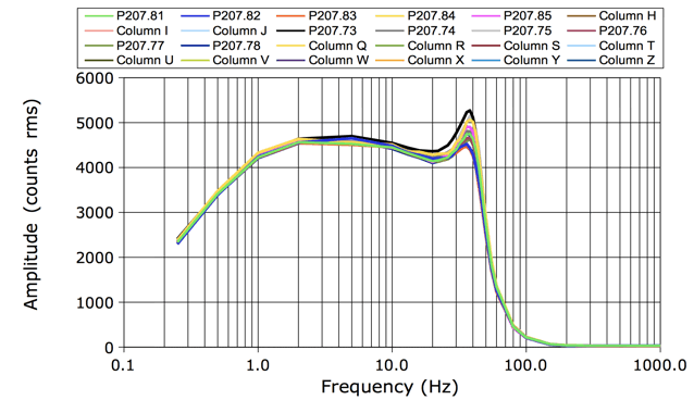
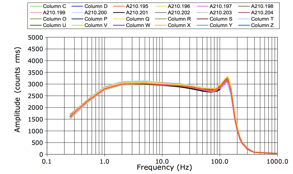