Implantable Sensor with Lamp (A3030)
© 2014-2021 Kevan Hashemi,
Open Source Instruments Inc.
Contents
Notice of Obsolescence
Description
Design
Modifications
Antenna Switch
Crystal Radio
Command Threshold
Command Reception
Reference Clock
Power Supplies
Boost Regulator
Lamp Modulation
Programmable Logic
Micropower Oscillators
Data Transmission
Battery Monitor
Battery Recharging
Analog Input
Sources of Lamp Artifact
Observations of Lamp Artifact
Lead Sealing
Separate EEG Monitor
Tunnel Grounding
Lamp Pin Corrosion
Batch ISL4C
Batch ISL5
Batch ISL6
Batch ISL7
Batch E157
Notice of Obsolescence
[27-JUL-22] The Implantable Sensor with Lamp (ISL) is obsolete. We have abandoned our attempts to combine sensor, stimulator, and light source into a single device. Instead, have separated them into an Implantable Stimulator-Transponder (IST), an Implantable Light-Emitting Diode (ILED), and a Subcutaneous Transmitter (SCT). We are retiring our Command Transmitter (A3029) as well, replacing it with command transmitters built into the Telemetry Control Box (A3042-B).
Description
[05-JAN-20] The Implantable Sensor with Lamp (A3030) contains a wireless EEG monitor and a radio-controlled stimulator for implanted light-emitting diodes (LEDs). The lamp itself will reside on a head fixture, such as the Head Fixture (A3024HF). The A3030's single-channel EEG monitor is similar to the Subcutaneous Transmitter (A3028P). The A3030's radio receiver is similar to the Implantable Lamp (A3024B). The stimulation machine on the A3030 we implement with a XO2-1200 programmable logic chip, which provides volatile and non-volatile memory as well as thousands of programmable logic gates. The A3030E, shown below, provides 915-MHz command receiver, 915-MHz data transmitter, amplifier, acknowledgment via 915-MHz auxiliary channel, battery voltage measurement via the auxiliary channel, and a 5-V lamp power supply.

Figure: Implantable Sensor With Lamp (A3030E, E157.5) Top Side. Orange L+ and purple L− terminated with a gold-plated 0.3-mm diameter pin, connect to lamp. Green lead is GND. Spring provides grounding for lamp current that escapes the head fixture. The black collars, when embedded in cement, reduce the current escaping the head fixture. The red X+ and blue X− are the EEG connections, terminated with a bare wires. The 50-mm antenna is for reception of commands and transmission of EEG data, acknowledgements, and battery voltage measurements.
The bare circuit board before encapsulation provides a programming extension and several test pins for us to calibrate the crystal radio and data transmitter.

Figure: Un-Encapsulated A3030E Circuit with Programming Extension. The large square component is the programmable logic chip.
We define the following versions of the A3030.
| Version |
EEG |
Features |
Battery
Capacity
(mA-hr) |
Volume
(ml) |
Shelf
Life
(months) |
| A3030X |
None |
None |
None |
1.7 |
53 |
| A3030A |
None |
None |
190 |
4.2 |
53 |
| A3030B |
512 SPS, 20 mV, 160 Hz |
146 MHz commands |
190 |
4.2 |
53 |
| A3030C |
512 SPS, 20 mV, 160 Hz |
910 MHz commands, acknowledgements |
190 |
4.2 |
53 |
| A3030C-LO |
512 SPS, 20 mV, 160 Hz,
no EEG leads (lamp-only) |
910 MHz commands, acknowledgements |
190 |
4.2 |
53 |
| A3030D |
512 SPS, 20 mV, 160 Hz |
910 MHz commands, acknowledgements,
random pulses |
190 |
4.2 |
53 |
| A3030D-LO |
512 SPS, 20 mV, 160 Hz,
no EEG leads (lamp-only) |
910 MHz commands, acknowledgements,
random pulses |
190 |
4.2 |
53 |
| A3030E |
512 SPS, 20 mV, 160 Hz |
910 MHz commands, acknowledgements,
random pulses, shared antenna,
battery-recharge diodes, battery monitor,
differential amplifier, ground connection |
190 |
4.5 |
53 |
Table: Versions of the A3030.
The A3030C/D versions receive commands at 910 MHz and transmits EEG samples in the 902-928 MHz band. It transmits acknowledgement messages when requested to do to by a command, so that we can confirm reception of stimulus commands. It is equipped with a lithium-ion battery and encapsulated in epoxy and silicone. The A3030C/D works well, but is plagued by lamp artifact caused by water carrying lamp voltage out of the head fixture and into the animal body, where it corrupts the EEG signal. Ceramic dual-bore collars around the lamp leads stop the water conduction, but the seal within the collar can still fail, and when it does, the EEG signal is compromised. Reception of commands by implanted A3030C/D transmitters tends to degrade with time, but acknowledgments transmitted by the devices permit us to determine when commands have not been received.
The A3030D-LO is designed to remove the concern of seal failure from an optogenetics experiment by removing the EEG pick-up leads altogether. We combine the A3030D-LO with a separate subcutaneous transmitter to monitor EEG. The EEG and lamp power circuits are now separated and their battery power supplies are floating with respect to the animal body. Failure of the collar seal will introduce some artifact into the EEG signal, but two orders of magnitude less than if the EEG X− lead is connected to the lamp power 0 V.

Figure: ISL Controller Tool. In addition to providing buttons to control ISLs, the program will monitor battery voltage automatically by issuing its own battery check commands. When battery voltage drops too low, the program turns off the ISL to avoid battery damage.
The A3030E provides a differential amplifier with a ground wire so that we can ground the animal body outside the head fixture. The ground connection provides a common-mode reference voltage for the differential amplifier. By placing the ground outside the head fixture, we allow it to absorb current traveling along the tunnels made in the head fixture by the lamp leads, and so stop this current from setting up an electric field in the animal body that we will detect as lamp artifact in our EEG signal. The A3030E antenna switch allows us to share a single antenna between the command receiver and data transmitter. Two diodes in the A3030E permit us to re-charge the battery through the lamp leads rather than piercing the encapsulation. A voltage divider in the A3030E permits us to measure the battery voltage directly so as to give us an indication of the remaining capacity. The voltage divider that generates the command detection threshold is more immune to corrosion, which we suspect is the cause of the degrading command reception by implanted transmitters. An isolated pad on the top edge of the circuit board allows us to solder a stiff wire to the assembled A3030E to hold the circuit while we dip it in epoxy in a vacuum and later rotate it while the epoxy cures.
Design
S3030X_1: Implantable Sensor with Lamp Initial Circuit.
S3030A_1: Implantable Sensor with Lamp Version A/B.
S3030C_1: Implantable Sensor with Lamp Version C.
S3030D_1: Implantable Sensor with Lamp Version D.
S3030E_1: Implantable Sensor with Lamp Version E.
Code: Logic Programs and Test Scripts.
LCMXO2-1200ZE: The programmable logic chip data sheet.
A303001A.zip: A303001A Gerber Files.
A303001A.pdf: A303001A All-Layer Circuit Board View from Advanced Circuits.
A303001B.zip: A303001B Gerber Files.
A303001B.pdf: A303001A All-Layer Circuit Board View from Advanced Circuits.
A3030B_SMT.pdf: A3030B Part Placement Drawing from Advanced Assembly.
A303001C.zip: A303001C Gerber Files for A3030E.
A303001C.gif: Panel 5 x 2 of A303001C.
ISL Controller Tool: A LWDAQ Tool that stimulates the ISL.
Modifications
[26-AUG-14] The A303001A printed circuit board requires the following modifications for the A3030A assembly. The A303001A PCB was designed to the S3030X schematic. The A3030A follows the S3030A schematic, except that the EEG amplifier and converter are omitted.
- Omit U8. Load a 10 kΩ P0805 resistor from the U8-2 pad to the U8-4 pad.
- Solder a 10 kΩ P0805 resistor between pins P1-7 and P1-8.
- Solder a CMDSH2-3 diode across C11, cathode to 0V.
- Component changes: C10 and C11 are 100 pF, Q1 is NDS355AN, C7 is 1.0 pF.
- Omit U6, U9, and associated capacitors and resistors of EEG amplifier.
[29-SEP-14] The A303001B printed circuit board is the same as the A303001A, but with the following changes as expressed in the S3030A_1 schematic.
- Omit U8 and replace with R23, 8.0 kΩ.
- Add R24, 8.0 kΩ.
- Add D2, CMDSH2-3 in SOD-323.
- Change C10 and C11 to 100 pF
- Change Q1 NDS355AN.
- Change C7 to 1.0 pF.
- Omit R19, R20, C21, C22.
- Round off the circuit board corners.
- Omit toroidal footprint for L2.
- Change C15 to 8p0.
- Change R8, R21, R22 to 33 kΩ.
[06-MAY-15] The A3030B on an A303001B PCB becomes an A3030C with the following modifications as expressed in the S3030C_1 schematic.
- R5 and R6 drop from 1 MΩ to 10 kΩ.
- C15 increases from 10 pF to 1.0 nF.
- C16 increases from 100 nF to 10 μF.
- R7 drops from 10 MΩ to 100 kΩ.
- Tuning: C7 = 0.5 pF, C8 = 0.5 pF, C9 = 2.7 pF, L1 = 0 nH.
Unlike earlier versions, the A3030C has the same tuning capacitances for all circuits we assembled. The tuning at 915 MHz is not nearly so sharp as it was at 146 MHz.
[24-JUN-15] The A3030D circuit is the same as the A3030C except for Q1, which we switch to the NTR4003. The A3030B on the A303001B PCB becomes an A3030D with the following modifications as expressed in the S3030D_1 schematic.
- R5 and R6 drop from 1 MΩ to 10 kΩ.
- C15 increases from 10 pF to 1.0 nF.
- C16 increases from 100 nF to 10 μF.
- R7 drops from 10 MΩ to 100 kΩ.
- Tuning: C7 = 0.5 pF, C8 = 0.5 pF, C9 = 2.7 pF, L1 = 0 nH.
- Q1 becomes NTR4003N.
[30-AUG-17] The A3030E assembled on the A303001C printed circuit board requires the following modifications.
- Load C9 100 pF P0402 between X+ and X−, and C15 100 pF P0402 between X− and 0V, as shown here. Perform this modification before you load the leads.
Antenna Switch
[17-JUL-18] The A3030E introduces U14, the PE4239 antenna switch that allows us to connect only one antenna to the circuit. We power the switch logic with VSY from which it draws 200 nA. With U10 turned off, input XEN is low, and the crystal radio is selected. When U10 is turned on, it asserts XEN to turn on U11 for data transmission, and this same signal connects the antenna to A, the U11 output.
[25-AUG-17] The antenna switch functions perfectly, switching between data transmission and command reception. We must connect power to the A3030E in order to enable the switch so that we can test the crystal radio, which contrasts with the A3030D and earlier, in which we could test the crystal radio with no power connected.
Crystal Radio
[23-JUL-14] The Crystal Radio detects 146-MHz radio waves without any external power supply. It consists of a two-turn, 30-mm diameter loop antenna connected to terminals B and G, and components C7-C11, L1, D1, and D2. The circuit is identical to the crystal radio we used in the Implantable Lamp (A3024B), except it uses two tuning diodes instead of one, in an effort to increase the sensitivity of the command receiver. A split-capacitor tuning network selects and amplifies 146-MHz power from the antenna and applies it to the tuning diodes. Capacitor C10 allows a demodulated voltage on L1 so the second tuning diode, D1-1-3, can contribute to VR.
As we describe in Antenna Matching, we must measure the tank resonant frequency of our tuning network, then adjust the tuning capacitance until the resonance is close to 146 MHz. We use our 146.000-MHz crystal oscillator to provide a reference frequency. We apply a voltage ramp to the TUNE input of our Command Transmitter (A3023CT). We attenuate the +22 dBm output of the A3023CT's by 6 dB and split it in two. One part goes through a 12-dB attenuator to a wire stub, around which we will place our crystal radio antenna. The other part passes through a 3-dB attenuator to the LO input of a mixer. We take our −4 dBm 146.000 MHz and pass it through a 150-MHz low-pass filter to remove the harmonics. We apply the resulting 146.000 MHz sine wave to the RF input of our mixer. The intermediate frequency (IF) we pass through a 3-dB attenuator and a 22 MHz low-pass filter, and then to the oscilloscope. We connect a probe to the VR terminal on our A3030X No1.1 and observe the tuner's response. We turn on the oscilloscope's 20-MHz bandwidth limit so that we can see the response of VR without the RF overlaid.
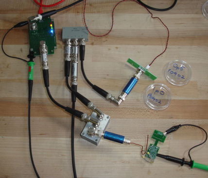
Figure: Crystal Radio Calibration Set-Up. An A3030X with Crystal Radio components and pick-up antenna receives sweep frequency from a wire stub.
We load 0.5 pF for C7, 8.0 pF for C8, and 1.5 pF for C9. We obtain the following response on VR. The bottom trace is the IF output of our mixer. The point where the IF frequency is zero is the point where the sweep frequency is exactly 146 MHz. This point is visible on the oscilloscope as a fluctuating slice in the IF trace. We have aligned this slice with the center of the screen. The limits of the IF trace show ±20 MHz.
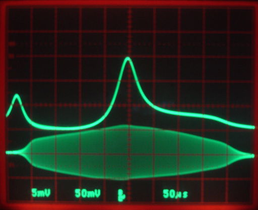
Figure: Antenna Tuning, No1.1, C7 = 0.5 pF, C8 + C9 = 9.5 pF. Bottom trace is IF from mixing 146.000 MHz with the sweep frequency. Top trace is VR with a wire stub carrying the sweep frequency passing through the Crystal Radio's loop antenna, 50 mV/div from our ×10 probe, 50 μs/div. The sweep frequency is 146 MHz at the center of the screen and increases by 5 MHz/div.
The tank resonance is at 145.5 MHz. The antenna resonance is the smaller peak down at 123 MHz. If we squeeze the antenna, the antenna resonance disappears. By enclosing the antenna in one hand, we are able to move the tank resonance down to 145.0 MHz. The 90% width of the peak is 2 MHz wide.
We disconnect the sweep, make sure the A3023CT emits 146.0 MHz, connect an whip antenna to its output, push the whip antenna through the A3030X's loop antenna, and generate 1-ms pulses of radio frequency power. We see 800-mV pulses on VR. The 99% rise time of the pulses is 40 μs and the fall time is 44 μs. For 80-mV pulses on VR, rise time is 40 μs and fall time is 22 μs.
[25-JUL-14] We set C7 = 1.0 pF, C8 = 8.0 pF and C9 we omit. Tuning is as shown below.
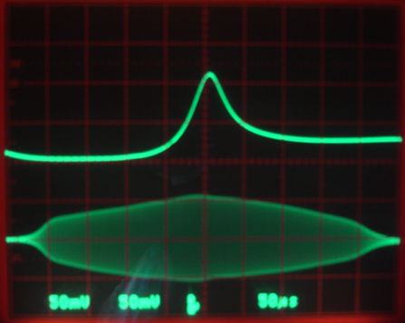
Figure: Antenna Tuning, No1.1, C7 = 1.0 pF, C8 + C9 = 8.0 pF. Bottom trace is IF from mixing 146.000 MHz with the sweep frequency. Top trace is VR with a wire stub carrying the sweep frequency passing through the Crystal Radio's loop antenna, 50 mV/div from our ×10 probe, 50 μs/div. The sweep frequency is 146 MHz at the center of the screen and increases by 5 MHz/div.
The peak is at 147 MHz. When we load 0.5 pF in C9, the peak drops to 144.5 MHz. We remove C9 and peak returns to 147 MHz. The width of the peak is 3 MHz. When we compare our A3024 single-diode tuner to this dual-diode tuner, we we get roughly double the peak amplitude, which is what we were hoping for. For each 1 pF we add to the sum of C8 and C9, we drop the tank resonance by 5 MHz. With 0.5-pF capacitors, we can tune our crystal radio to within 1.2 MHz of 146.0 MHz.
[11-AUG-14] We switch C10 and C11 to 100 pF to speed up the falling-edge response of the command threshold circuit. We see no increase in the RF power we observe on VR, and observe no other ill effects of the reduction in decoupling capacitance.
[30-NOV-14] For ISL Stage 6 we plan to move from 146 MHz command frequency to 915 MHz. The following graphs show the tuning circuit gain around 915 MHz for various new values of tuning capacitor and inductor. We also vary what we imagine will be the effective resistance of the antenna.The diode resistance is the video resistance of the two diodes in parallel.
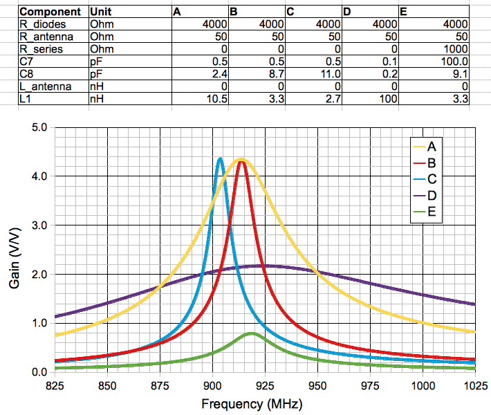
Figure: Calculated Voltage Gain of the Tuning Network for Various Lumped Component Values.
[01-DEC-14] We solder a 50-mm insulated, stranded steel wire to B as our command antenna. We apply a −5 dBm 830-1100 MHz sweep to an A3015C loop antenna. We mix the sweep frequency with 910 MHz and pass the result through a 21-MHz low-pass filter to give us an intermediate frequency that crosses through 0 Hz when the sweep is at 910 MHz, and vanishes to zero outside 890-930 MHz. In the trace below we see this IF, and below it VR with the A3030C antenna 1 cm from the A3015C.

Figure: Measured VR vs. Frequency. The bottom trace is 5 mV/div obtained with a ×1 probe on VR. The top trace shows 890-930 MHz, with the zero-crossing at 910 MHz.
To obtain tuning shown above, we have C7 = 0.5 pF, C8+C9 = 1.8 pF, L1 = 2.7 nH. When we add to C8+C9 the capacitance of the two tuning diodes, we get 2.4 pF as an estimate of the capacitance in parallel with L1. Plot A in the calculations above is for these values and L1 = 10.5 nH. Our 2.7-nH inductor is one turn around a P0805 package. The tracks leading to and from L1 are four times longer. It appears that the effective inductance of L1 and the tracks leading to it, between it and C10, and from C10 to 0V, act like a 10.5-nH inductor, thus giving us the shape we photographed above, which matches trace A.
We apply 13 dBm of 910 MHz to an A3015C loop antenna. This antenna has its own 3-dB stabilizing antenna. We hold our A3030C at range 30 cm and rotate at random. We obtain ≥20 mV on VR, which is sufficient for command reception. With +30 dBm, assuming an inverse square law of power distribution, we expect to obtain the same reception at range 2 m.
[05-MAR-15] We apply an 840-980 MHz sweep to our new 915-MHz Command Transmitter (A3029B). We get roughly 22 dBm of the same sweep, which we connect to a Loop Antenna (A3015C), which has its own 3 dB stabilizing antenna. We try various combinations of C7, C9, and L1. The following trace is for C7 = 0.4 pF, C9 = 2.7 pF, and L1 = 0.0 nH. We load a 0 Ω resistor in place of L1. The transmit and receive antennas are 30 cm apart.
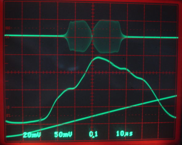
Figure: Measured VR vs. Frequency. The bottom trace is 20 mV/div obtained with a ×1 probe on VR. The top trace shows 840-980 MHz, with the zero-crossing at 910 MHz.
When we load 2.7 nH for L1, the peak of this response drops from 920 MHz to 850 MHz, which suggests that the parasitic inductance of our PCB traces is around 11 nH. If we add 1.0 pF to C9, the peak drops from 920 MHz to 890 MHz, which suggests the parasitic capacitance of our traces and the crystal diode is around 10 pF. After many component changes, we settle upon C7 = 0.5 pF, C9 = 2.7 pF, and L1 = 0.0 nH, with response indistinguishable from that shown above.
We place transmit and receive antennas in our small faraday enclosure (35 cm side), and in a larger enclosure (75 cm side) and obtain robust reception across the enclosure diagonal in both cases.
[19-MAR-15] We use the Diagnostic Instrument and an A3029B to produce 120-μs pulses of +29.4 dBm 915 MHz, which we feed into an A3015C loop antenna. Our A3030C tuned to 915 MHz produces ≥10 mV pulses on VR in 95% or orientation at range 100 cm.
[25-MAR-15] The data and command antennas of our A3030C are straight and parallel, separated by one or two millimeters along their 50-mm lengths. We turn on data transmission and observe VR and TCK. The latter signal is the 5-MHz clock that drives data transmission.

Figure: Self-Reception at 915 MHz. Top trace is VR recorded with ×1 probe, 20 mV/div. Bottom trace is TCK recorded with ×10 probe, 1 V/div. Time is 2 μs/div. The data transmission lasts for 7.7 μs, after which TCK continues to run until the end of the RCK period.
The 915-MHz data transmission causes 915-MHz reception by the crystal radio. The pulse on VR is well above our 10-mV command threshold. We get a pulse on RP that begins roughly 5 μs after the data transmission and endures for roughly 20 μs. A 20-μs pulse like this on RP during command reception is likely to corrupt the command. In the A3030C firmware, we disable transmission during command reception.
[22-APR-15] We have seven assembled A3030Cs with both antennas and all four leads. We have C7 = 0.5 pF and C9 = 2.7 pF. With all leads attached, the resonant frequency of the seven matching networks, including that of No1, have risen to 950±20 MHz. We add C8 = 0.5 pF to all circuits. After washing and drying, resonant frequencies are 915±20 MHz. The resonant peak itself is 120 MHz wide between its 70% points, so each matching network is well within tolerance for 915-MHz reception.
[26-AUG-17] We have A3030E circuits on the A303001C layout, which we designed for operation at 910 MHz in conjunction with an RF switch to permit the sharing of a single antenna between the radio and the transmitter. All inductors and capacitors are P0402.
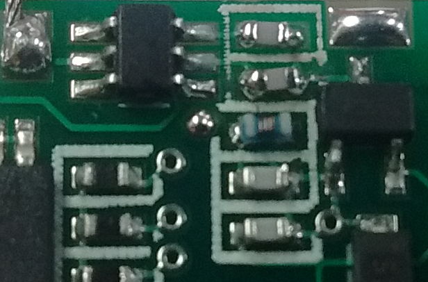
Figure: The A3030E Crystal Radio. From top to bottom in the middle we have C7, C8, L1, C10, and C11.
We lay a A3015C loop antenna on our bench with the A3030E on top and a ×1 probe measuring VR. We attach a battery so that the RF switch will be open for the radio. We drive the antenna with 0 dBm (1 mW) of variable frequency using our SSG-6001 signal generator. With C7 = 0.5 pF, C8 = 0.5 pF, and L1 = 3.3 nH we get a peak of 33 mV on VR at 1650 MHz.
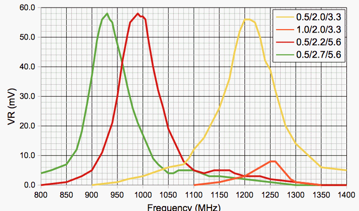
Figure: Response of the A3030E Crystal Radio for Various Matching Networks. Each plot is named after the values of C7/C8/L1.
We also tried a 0.5/2.2/5.6 network and found the peak to be at 970 MHz. With network 0.5/2.7/5.6 we obtain reliable command reception at ranges up to 50 cm to one side of an A3015C command antenna.
[29-AUG-17] We place the straight 50-mm antenna of various A3030D/E crystal radios 10 cm from an A3015C command antenna driven by 10 dBm of 800-1000 MHz. The loop antenna is standing up on our bench top and the antenna is lying on the bench surface, parallel to the plane of the loop antenna. We compare the A3030D tuning to that of the A3030E. We find that the arrangement of the lamp and EEG leads can change the value of VR by a factor of four. We try to keep the same arrangement each time. The A3030D we tested has no lamp or EEG leads.
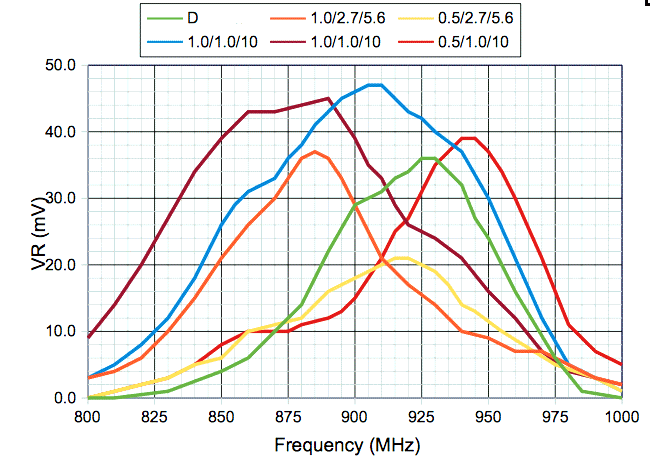
Figure: Response of Various Matching Networks. Plot D is the A3030D, the others are A3030E named after C7/C8/L1.
The two plots 1.0/1.0/10 are for E157.1 and E157.2 loaded with the same matching network. The peak for E157.1 is exactly right: at 910 MHz, but that of E157.2 is at 890 MHz. The 0.5/1.0/10 plot is for E157.2 after we drop C7 from 1.0 pF to 0.5 pF. Both 1.0/1.0/10 networks give 95% command reception for varying orientation at range 80 cm from the command antenna. We compare this to 80% reception by encapsulated D7.9. The maximum range for command reception with the 1.0/1.0/10 network is 190 cm with straight antenna and 220 cm with bent antenna. Command reception at range 80 cm with the bent antenna is also 95%.
[19-SEP-17] We tune the crystal radios of E157.3-E157.14. Half of them we have to adjust because their peak frequency is below 890 MHz and reponse at 910 MHz is less than 80% of maximum. To raise the frequency, we drop C7 to 0.5 pF, and if we have to drop it after that, we add 0.2 pF to C8. All now have peaks similar to the 1.0/1.0/10 blue trace above. In order to obtain a good measurement of the response, we must not be holding the circuit board, so we prop it up 30 cm from an A3015C driven by 10 dBm and hook a thin wire into the VR test pad and measure with a ×1 probe.
Command Threshold
[24-JUL-14] The Command Threshold generates a logic HI when the Crystal Radio's VR is greater than the threshold. The threshold runs off the standby power supply, VSY, which we obtain from the battery voltage, VB, with regulator U1, a TPS70930. The threshold is set to roughly 10 mV by R3, R4, and C12. The comparator is U4, an MCP6541. Its output is RP (Radio Power), and drives an OR gate, U5. When RP is asserted, U5 generates WK (Wake), which turns on the 3V0 and 1V2 power regulators. The logic chip, U10, accepts RP and also generates OND for U5. Thus U5 asserts WK whenever there is RF power and whenever U10 asserts OND.
We assemble the standby power supply and the Command Threshold on No1.1. We connect OND to 0V. By pulsing 146-MHz power we observe pulses on WK. Quiescent current from VB = 3.3 V with no pulses is 1.9 μA. With 1 ms pulses at 500 Hz it is 2.0 μA. We load 25 kΩ for R4, which puts the threshold at around 8 mV.
[11-AUG-14] We transmit +30 dBm pulses with our A3029A. We have C10 and C11 at 100 pF. With the pick-up coil in a favorable orientation 30 cm form the transmit antenna, we see 3-V pulses on VR. After such pulses, it takes hundreds of microseconds for VR to return below the command threshold. We tarnsmit 122-μs pulses every 244 μs (a 4.096 kHz clock). The RP signal goes HI within a few microseconds of the start of a pulse, but its return to LO after the end of the pulse takes longer than 122 μs when VR exceeds 1 V.
[13-AUG-14] We place a CMDSH2-3 Schottky Diode across C11 so as to limit the value of VR during powerful pulses. With +30 dBm transmit antenna at range 0 cm, VR does not exceed 100 mV. With maximum input power, the delay between VR and RP is < 1 μs on the rising edge and 45 μs on the falling edge. With input power just above threshold, the delay is 10 μs on the rising edge and 34 μs on the falling edge.
[27-AUG-14] We remove the Schottky diode across C11 and transmit commands to the A3030X. We have 30 dBm of RF power being transmitted by a half-wave antenna. At ranges closer than 10 cm, command reception fails. At Range 1 m, we get reception in all orientations. At range 3 m, in most orientations. At 10 m we get reception if we touch the loop antenna. We restore the diode. At ranges 0-100 cm reception is reliable in all orientations. At higher ranges, performance is the same as without the diode.
[09-SEP-14] We change R4 from 33 kΩ to 16 kΩ in A3030A No1.8 to see if this will increase its operating range. With +30 dBm output power into a half-wave antenna, reception is reliable at 100 cm before and after the change. Reception with A3024B-M No2.5 is similar. We leave the 16 kΩ in place of R4. We'll see if this one gives better performance when implanted. When we walk around with the lamp pins in our mouth instead of attached to a lamp, we get reception up to 15 m away.
[18-JUL-17] We used 33 kΩ for R4 and 10 MΩ for R3 in all A3030C/D circuits. The nominal threshold voltage was 10 mV. We wanted to accommodate the ±7 mV maximum input voltage offset of U4. But reception by the implanted devices was not robust. Moving the antenna to give a more powerful signal improved reception. The U4 data sheet says the typical input offset voltages is ±1.5 mV. We could use R4 = 16 kΩ with R3 = 10 MΩ and expect a threshold of 4.3-6.3 mV.
Command reception degraded for implanted transmitters as time went by. One reason this may happen is the resistance of R4 starts to drop because of corrosion between its terminals. One of the first signs of corrosion in subcutaneous transmitters is a drop in input impedance from 10 MΩ to 1 MΩ after the equivalent of one or two years implanted. If the R3 dropped to 1 MΩ, the threshold voltage would rise to 50 mV and sensitivity would be greatly reduced. In the A3030E we resolve to drop R3 to 1.0 MΩ and accept a 3-μA addition to the standby current. We set R4 to 2.0 kΩ and so put the threshold at around 6 mV. A corrosion resistance of 1 MΩ would raise the threshold to 12 mV.
Command Reception
[13-AUG-14] The following timing diagram shows our prototype command transmission protocol. The protocol is designed to be robust in the face of 146-MHz interference and loss of signal power at the receiving loop antenna. The protocol permits us to transmit an arbitrarily large number of bytes. The receiver must store these bytes in memory, and when the transmission is done, compare the final two bytes to a checksum of the rest of the bytes. If the checksum is invalid, the receiver will ignore the transmission, on the grounds that it could be interference.
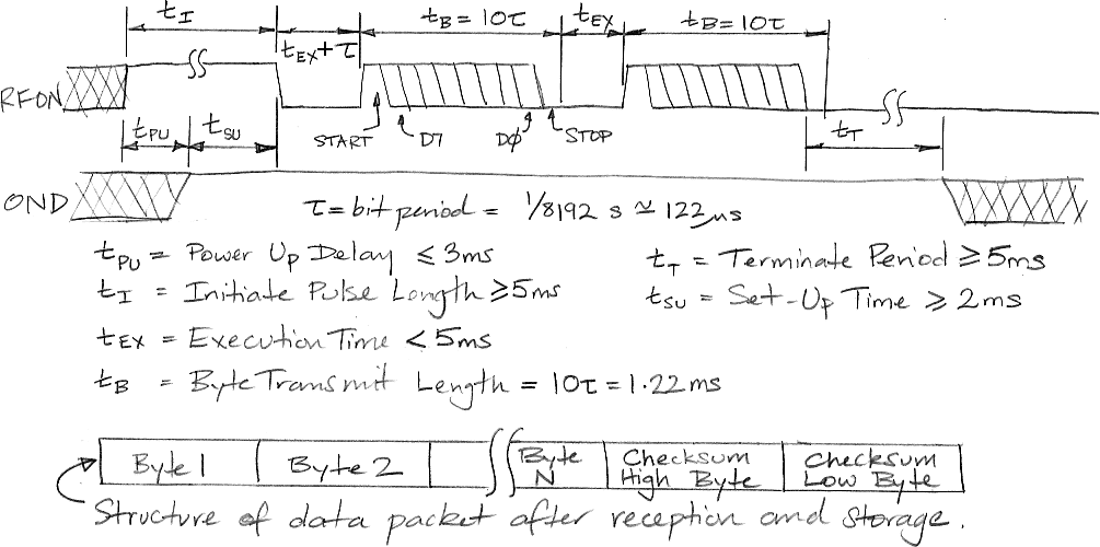
Figure: Command Transmission Protocol.
The command transmission begins with the initializing pulse, which lasts for tI ≥5 ms. The receiver may be inactive at the start of this pulse, so the pulse allows sufficient time for the receiver to power up and assert OND (ON Device) signal. This takes time tPU < 3 ms. Once OND is asserted, the receiver monitors the state of RP (Radio Frequency Power). The receiver samples RP on the rising edge of RCK, a 32.768-kHz ±20 ppm clock. When RP has been asserted continuously for tSU ≥ 2 ms, the receiver asserts IC (Initiate Command).
To begin data transmission, the transmitter turns off the RF power for a time tEX + τ. The time tEX is the time we allow the transmitter to prepare to send the next data byte. We allow tEX between each byte transmission as well. We must have tEX < tI = 5 ms or else the interval between bytes will be mistaken by the receiver as a termination period. At the end of the initializing pulse, we must have at least one bit period (122 μs) with no RF power so that the receiver can get ready for the first byte's start bit.
The bit period for serial transmission is τ = 4/32768 = 1/8192 = 122 μs, which is four periods of RCK. A serial byte begins with a start bit, which is HI, the data bits, most significant first, and a stop bit, which is LO. One byte takes 10τ = 1.22 ms. With tEX = 0 μs we attain the maximum data rate of 820 Bytes/s. If, at the end of the serial byte, the receiver does not observe a stop bit, the transmission is either interference or it is a genuine command transmission corrupted by loss of signal power. In either case, the receiver should abort command reception and go back to waiting for an initializing pulse.
When the last byte has been received, the transmitter turns off power for at least 5 ms, which indicates to the receiver that the transmission is complete. The receiver asserts TC (Terminate Command). The receiver analyzes the sequence of received bytes. If the checksum is incorrect, the receiver ignores the transmission. If it was inactive before reception, it un-asserts OND. If the checksum is correct, but the data itself contains errors, the receiver can take some action, such as transmitting a channel-fifteen message on its data transmitter.
We use an A3029A with firmware version 3 to implement the command transmission protocol. We begin with a 5-ms pulse of RF power, which allows the logic chip on the A3030 plenty of time to power up and detect 2-ms of continuous RF power, which is the token for the start of a transmission. After this long pulse, there follows a low pulse less than 5 ms long, and then a command. The traces below show VR and RP during reception of byte data values "0 170 0 255". To transmit these bytes with a A2037E LWDAQ Driver, we use our command transmit Toolmaker script.
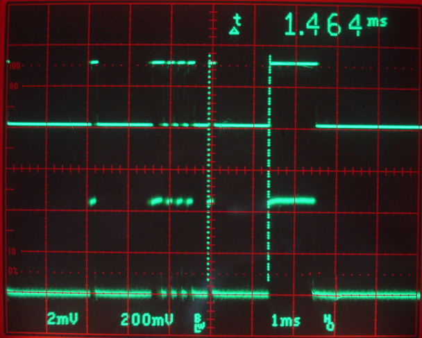
Figure: Command Reception in the A3030X. Top trace is RP at 2 V/div. Bottom trace is VR at 20 mV/div. The trigger is on the falling edge of the 5-ms initiating pulse.
The time markers show the byte transmission rate. We allow a slight delay between the stop bit of one byte and the start bit of the next. The result is 1.5 ms per byte, or 670 bytes/s.
[14-AUG-14] With firmware P3030X07.vhd we implement command reception in the logic chip, so that we generate a pulse NCS (New Command Strobe) at the end of each transmitted data byte. We also have TC (Terminate Command), IC (Initiate Command), and RXC (Receive Command) signals working correctly.
[18-AUG-14] With firmware P3030X08.vhd we implement command decoding, so we can send commands to turn on and off the lamp, activate, or deactivate the A3030X. The traces below show VR, CSB (Command Start Bit), and RPS (Radio Power Synchronized).
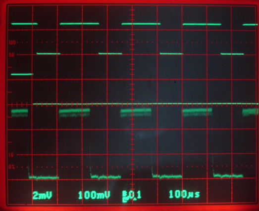
Figure: Command Reception in the A3030X. Top trace is RPS at 1 V/div. Bottom trace is VR at 20 mV/div. Center trace is CSB at 1 V/div. The trigger is the rising edge of CSB. The command is decimal value 85.
We generate RPS with a register clocked on the falling edge of RCK. The delay between a rising edge on RP and a rising edge on RPS is, in the traces above, less than 10 μs, while the delay between falling edges is closer to 45 μs. As a result, the positive pulses of RPS are longer than the negative pulses.
We attach a battery to our A3030X, connect boost power to our A3029A, and a half-wave antenna. With the receiving loop antenna of the A3030X in air, and the device held between two fingers, we flash a blue LED reliably by means of commands in all orientations up to range 1 m. We obtain some response up to 3 m. With the loop antenna in hand, we obtain reliable reception at 3 m and some response at 10 m.
[22-AUG-14] We trigger on the BITS (bit strobe) signal of our P3030X09.vhd firmware, and compare it to RP on our A3030X. We are interested in the position of the rising and falling edges of RP with respect to the falling edge of BITS.
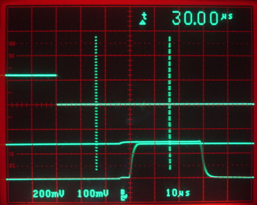
Figure: Command Bit Timing in the A3030X. Traces from many bits overlaid. Top trace is BITS at 1 V/div. Bottom trace is RP at 2 V/div. Timebase is 10 μs/div. The two time markers show the extreme positions of the rising edge on RP.
When RP enters the logic chip, we synchronise it with the reference clock, RCK using the RCK falling edge, and so generate RPS. The falling edge of BITS is when the Byte Receiver takes in the value of RPS. Thus we sample RP for byte reception half an RCK period (15 μs) before the falling edge of BITS.
The rising edges of RP can occur immediately after the falling edge of RCK, in which case there will be a 30-μs delay before RPS shows a rising edge. Or RP's rising edge can occur immediately before the falling edge of RCK, in which case RPS will immediately show the transition. When the RP transition occurs exactly on the falling edge of RCK, the state of RP is uncertain. It might rise immediately, or it might not rise until the next falling edge on RCK. Thus we expect to see the rising edges of RP span 30 μs as the 32.768-kHz clock on the Command Transmitter drifts with respect to the 32.768-kHz RCK on the A3030X. This is exactly what we see, along with stuttering between the two extremes when RP is synchronous with RCK. The markers on the picture show the two extremes of the RP rising edges.
The traces also show clearly the difference between the rising and falling edge response of RP to VR. In this case, they are separated by about 30 μs. For both rising and falling edges, however, we have at least 45 μs of set-up time before we sampel RP (this point being 15 μs before the falling edge of BITS) and at least 30 μs of hold time. With this we are well-satisfied.
Our P3030X09.vhd is debugged and working, with the exception of the CRC error check. Command bytes are received, stored to RAM, read back, and executed. We use the ring oscillator to provide modulation of the lamp, so as to create varying intensity. The stimulus controller is working well, but it does not provide randomized pulses.
[25-AUG-14] The sixteen-bit cyclic redundancy check is now working in P3030X10.vhd. We pre-load the CRC to all ones so that the checksum for a solitary zero command is not itself two zeros. We prepare the ISL Controller Tool V2. We run it from the LWDAQ Tool Menu and you get this window. The tool composes the string of command bytes that will configure the ISL to perform the stimulus specified in the parameter boxes of the tool window. It calculates the checksum for the byte sequence, and appends it as two further bytes to the command bytes. When we press Stimulate or Stop, the tool prints the commands and checksum to the screen. If we press Print, the tool writes a script to the text window. This script we can execute in any procedure or in the Tcl console to generate the same stimulus as we obtain when we press the Stimulus button. We can use the Print button to create the stimulus script we need for a Neuroarchiver event handler, so we can generate the stimulus when we detect an event in a live EEG recording.
[25-MAR-15] We place a Loop Antenna (A3015C) in a Faraday Enclosure (FE2A). There is an absorber on the floor. We supply commands from our 915-MHz Command Transmitter (A3029B). We program an A3030C with firmware C01. We bend the 50-mm receiving antenna on the A3030C into a loop. We transmit a command to flash the lamp once, and repeat this command at around 20 Hz. We move the A3030C around in the enclosure for 60 seconds and observe a total of 2 s of loss broken up into around six different intervals. So we appear to have 97% reception of commands within the enclosure.
Reference Clock
[24-JUL-14] The reference clock is a 32.768 kHz, ±20 ppm oscillator running continuously off VSY. It produces a 32.768 kHz square wave for command reception and message transmission. The ASH7KW oscillator draws less than 2 μA, but takes 500 ms to start up. We cannot turn it off, because the reference clock must be available and stable when the board wakes up to receive a command. The clock output enters AND gate U8, which delivers the clock to U10 only if the 3V0 power supply is turned on. If we delivered RCK directly to U10, we would consume excessive current when U10 was not powered up.
[31-JUL-14] We replace U8 with a 1-MΩ resistor from U7-1 to U10-35. Current consumption with WK unasserted is 4.0 μA. We also have U10 loaded. Now we assert WK and look at the 1-MΩ charging and discharging the input capacitance of U10-35 with a time constant of around 20 μs. We have configured this input to have no pull-up or pull-down or hold circuit, but with large hysteresis. The time constant implies an input capacitance of 20 pF. The data sheet says 6 pF. We have programmed U10 so that TP1 is RCK. We see 32.768 kHz on TP1 with no glitches, which means the hysteresis on the RCK input is working.
[08-AUG-14] The inactive current for our A3030X is 4.1 μA with a 1-MΩ resistor in place of U8. We try a 10-kΩ resistor. Inactive consumption is 4.4 μA. Where RCK enters U10, we see a 3-V square wave whose corners are rounded with a 320-ns time constant. When U10 is off, its inputs are high-impedance. The input capacitance is around 30 pF. We observe the same high-impedance at U10's RP input. We turn on the circuit with 1-ms RF pulses at 100 Hz. We have U10 powered up continuously. Active current consumption is 61 μA
Power Supplies
[25-JUL-14] Aside from VSY, we have 1V2 for the core of U10, 3V0 for the transmit oscillator, VA for the amplifier and ADC, and VC for the analog input. We load U2, U3, and associated capacitors and resistors. With WK unasserted, these voltages are all zero after we power up. When we transmit RF power to assert WK, the four power supply voltages turn on. Capacitors C3, C4, C5, and C6 charge up. When we unassert WK, with no circuits loading the power supplies, we find the capacitors remain charged up for several minutes.
We have the Command Threshold, Reference Clock, and Power Supplies loaded on the board. We wash, dry, and bake for an hour before making our current consumption measurement. Quiescent current from VB = 3.3 V with WK unasserted is 4.1 μA. We assert WK and current consumption rises to 5.3 μA. We unassert WK and consumption drops to 3.6 μA. The power supplies remain stable for several minutes. We can measure them with a 10-MΩ probe and observe discharge of the capacitors with time constant 100 s. After one minute, current consumption begins to rise at roughly 1 μA/s, and continues to rise. When the current reaches 200 μA we observe 3V0 to be 1.5 V and 1V2 to be 0 V. We assert WK and current drops to 5.3 μA. We unassert and it drops to 3.6 μA. After one minute, current consumption begins to climb again. We have 3V0 at 2.5 V and 1V2 at 0 V. We discharge C3 with tweezers and current consumption drops to 4.1 μA. We do not understand what is happening, but we figure that even 1 μA of quiescent current on 3V0 and 1V2 will discharge the capacitors in a few seconds, so this mysterious battery drain will not occur in the completed circuit.
[30-JUL-14] We load U8 with an AND gate. We restore broken OND tracks with wires, so OND is now available on the programming extension. We can connect it to VB with a jumper to turn on the board. We have 50 kΩ for R21 and R22. After twenty-four hour bake, we have 3.5 μA battery current with WK unasserted. We wait five minutes. Current remains 3.5 μA and 3V0 remains 0 V. We assert OND. We now have RCK at the output of U8. We have U10 loaded, so current from VB is around 5 mA. We unassert OND. Battery current drops to 5 μA briefly, then climbs. We observe 3V0 is 2.0 V instead of 0.0 V and is turning on the output of U8. In this version of the circuit, we have U8-1 wired to 3V0. We have RCK on U8-4. We short 3V0 and current drops to 3.5 μA and remains there. We conclude that we should connect U8-1 to WK, not 3V0, and we are not sure why we didn't do this in the first place.
[08-AUG-14] Our inactive battery current is now 4.0 μA and active current is 61 μA. When inactive, we drive U11's RCK input through 10 kΩ, thus eliminating U8. When active, this same 10 kΩ drives the RCK input fast enough to avoid loss in the the RCK input's Schmitt Trigger. With 1 MΩ in in place of U8, this loss was 50 μA. When the A3030X unasserts OND, it takes 700 ms for its active current to drain the 1V2 decoupling capacitors to the point where U11 shuts down.
[08-OCT-14] The A303001A and A303001B circuit boards are both designed for connection to a GM382030 lithium-polymer battery. This battery's source impedance is less than 60 mΩ. When we turn on the A3030A's lamp, we draw roughly 65 mA from the battery, for which the battery's output voltage will drop by less than 5 mV. The battery's typical capacity is 190 mA, so when fully charged, it will provide 62 mA for 3 hr continuously.
[07-JUL-15] We program 12 A3030D circuit boards. We discover an error in the P3030D04 firmware, and change our calculation of SRUN so that OND no longer remains asserted after a STOP or XOFF instruction.
Boost Regulator
[25-JUL-14] The boost regulator provides 5 V for the lamp. It boosts VB, which will be 3.3-4.2 V from a lithium-polymer battery, to 5 V using U12, an LTC3525-5, and L1. The ENL signal from logic chip U10 turns on the 5 V power. Transistor Q1 is a switch for the lamp cathode, which allows us to modulate the lamp current with signal ONL so as to produce an effective dimming of optical output.
We load the U12, L1, and Q1. We connect ENL and ONL to WK. With WK asserted, we transmit continuous RF power to assert WK continuously, and observe roughly 44 mA through 50-Ω of steel wire into a white LED. Current consumption from VB = 3.3 V is 72 mA, which suggests roughly 90% conversion efficiency.
We connect a 3.0-V lithium primary cell to the circuit and move it around while pulsing 1 W of RF power for 1 ms at 100 Hz. We carry the circuit around the lab. We obtain reception in favorable orientations at 10 m and in all orientations at 1 m.
[18-AUG-14] We connect a blue LED and a 100-Ω resistor to L+/L−. We supply 3.6 V to the A3030X. We turn on the lamp. The voltage on L− is 0.2 V, which is the drop across Q1. The voltage on L+ is 5.2 V. We have 2.0 V across the resistor and 3.0 V across the LED. That's 20 mA delivered from 5.2 V, or 104 mW generated by the boost regulator. The current drawn from the power supply is 31.4 mA for 113 mW. Efficiency is 92%.
[22-SEP-14] We have A3030A No1.1. We solder a 100-Ω resistor to the lamp output. For L2 we have the LQH32CN100K53 2.5 mm × 3.2 mm inductor we have used up until now, and in our work with the A3024. We supply 3.6 V battery voltage and turn on the lamp output continuously. Battery current is 78.2 mA. Lamp voltage is 5.0 V and the drop across Q1 is less than 50 mV. We have 130 mVpp triangular ripple on the 5.0 V at 100 kHz. The A3030A is 89% efficient at delivering energy to the lamp output.
We load a toroidal inductor, 83103C, for L1. This new inductor is far larger, being 5.2 mm × 5.9 mm. But we wonder if a toroidal inductor will produce less stray field, and so generate less noise in our EEG amplifier. When we switch on the lamp power, we get 5.0 V, 50 mA, 110 mVpp ripple at 100 kHz. But we draw 91.4 mA from 3.6 V, so efficiency is only 76%. We wash, repeat, and get the same result. We restore the previous, miniature inductor and get 89% again.
Lamp Modulation
[24-AUG-14] Transistor Q1 turns on and off the lamp in response to logic signal ONL from U10. We set U10 to drive 24 mA into the gate of Q1. We load an NDS355AN for Q1. When Q1 is on, 23 mA flows through the LED, 100-Ω resistor, and Q1. The voltage drop across Q1 is less than 10 mV. The traces below show the voltage across the resistor between the LED and the transistor drain while we are switching the gate at 1.0 MHz with a 20% duty cycle.
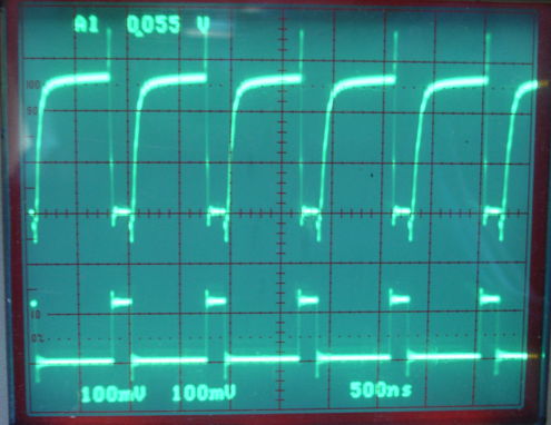
Figure: Lamp Modulation. Bottom trace is ONL as a 1.2-V logic signal on TP1. Top trace is the drain of Q1, 1 V/div.
Switch-on and switch-off both take around 20 ns, which is consistent with a 24-mA drive current and a 200-pF gate capacitance. The graph below shows how the average A3030X battery current varies with duty cycle of modulation when the lamp is modulated continuously. We have one grap for the NDS355AN, and another for the ZVN3306F.

Figure: Current versus Lamp Modulation Duty Cycle. The ZVN3306F has a 0.3-V drop across it with a current of 20 mA and gate voltage 3.0 V. The NDS355AN has a 0.0-V drop with a current of 23 mA.
Looking at the NDS355AN measurements, when the duty cycle is 0%, the current consumption is 740 μA. Of this, roughly 640 μA is the 150-MHz ring oscillator and 100 μA is the divider that reduces 150 MHz to 1 MHz. At 100% duty cycle, 23 mA is flowing through the lamp, L+ = 5.2 V, and we are drawing 34 mA from VBAT = 3.7 V. The boost regulator appears to be 95% efficient. If we take the slope and intercept of the 20% to 80% data points, we find the slope is 0.34 mA/% and the intercept is 4.6 mA. This intercept contains the 740 μA of the ring oscillator and modulation divider, but also the current required to charge and discharge the gate capacitance of Q1 at 1 MHz. The intercept of the ZVN3306F graph is indistinguishable from zero. The ZVN3306F's gate capacitance is only 35 pF. The ZVN3306F is more efficient at modulating the lamp power, but its 0.3-V forward voltage drop reduces the lamp current by 15%, which we find unacceptable. We prefer to load the NDS355AN into Q1.
[28-AUG-14] We connect a white LED to our A3030X through two 100-mm stretched helical stainless steel leads. We modulate the lamp intensity with 40% duty cycle. We place our scope probes on the L+ and L− outputs of the A3030X. We are looking for inductive voltage spikes induced by the leads.
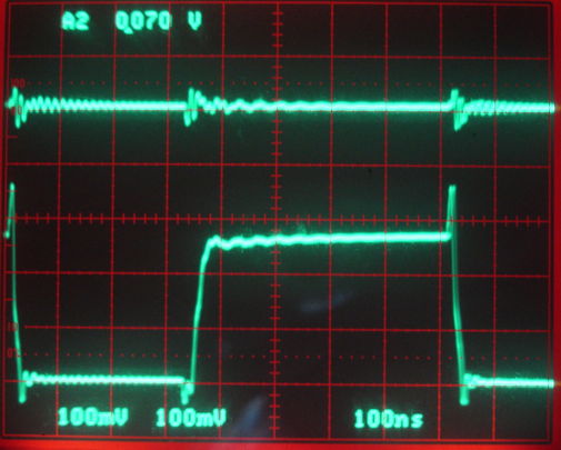
Figure: Lamp Modulation. Bottom trace is L−. Top trace is L+. Both are 1 V/div.
When the lamp switches on, L− experiences an initial positive spike. This spike is caused by the rising edge on ONL which is driving the gate of Q1 up to 3.0 V. As ONL charges the gate capacitance, charge is injected into the channel of Q1, causing a spike on the drain voltage. Within a few nanoseconds, however, the transistor is conducting to 0 V, and the drain voltages drops to 0 V. This spike does not represent any change in current flowing through the diode.
When the lamp switches off, we see no sign of an inductive voltage spike on L−. The helical leads present an inductance, but the 60-Ω resistance of the leads is sufficient to dampen any tendency of this inductance to cause a positive spike on L−. We check the location of the peak of the crystal radio response with the A3030E 30 cm from an A3015C powered by 10 dBm and find it to be 920 MHz rather than 930 MHz. We hold the A3030E with antenna straight down and bring a beaker of water up around the straight antenna. The value of VR varies from 5 mV with no water to 10 mV with half the antenna immersed to 5 mV with the entire antenna immersed.
[14-MAY-15] At ION, we demonstrate ISL Stage 6 and find that, with the ISL in water, flashing a lamp that is out of water, we get the same step disturbance of the EEG signal when we turn on lamp modulation. The EEG signal steps up by roughly 300 μV when the lamp is on, for all modulation other than 0% and 100%. As we show above, lamp modulation with the NDS355AN for Q1 draws 4.6 mA. The 3-V regulator that provides VA is the TPS970930. The same regulator supplies the 3-V power for ONL, the lamp modulation signal. When lamp modulation is anything other than 0% and 100%, the modulation logic draws 4.6 mA. According to its data sheet, the regulator output drops by 100 μV/mA, so we expect a drop of 460 μV in VA during modulation. But the average value of X is VC = 1.2 V, which will appear to jump up by 1.2 / 3.0 × 460 μV = 180 μV.
[17-JUN-15] We turn on sample transmission and initiate 10-ms lamp pulses at 10 Hz in an un-encapsulated A3030C. We have no lamp attached. With 20% to 80% modulation we observe 3000 counts of modulation-induced noise. We replace Q1 with NTR4003N, a mosfet with a 20-pF gate capacitance, which is ten times smaller than that of the NDS355AN. The modulation noise decreases to 150 counts. We try the FDV301N, a mosfet with 10-pF gate capacitance. Modulation noise is now 2000 counts. We return to the NTR4003N and get 100 counts, back to the FDV301N and get 1500 counts. We do not understand why the FDV301N produces noise out of proportion to its gate capacitance. The NTR4003N, however, looks like a fine choice for Q1. Its channel resistance is only 1.5 Ω, which is much smaller than our 60-Ω lamp lead resistance.
[24-JUN-15] We obtain this trace or random pulse noise from the A3030D with Q1=NTR4003N and 80% modulation, 10-ms pulses at 10 Hz average frequency.
[09-JUL-15] We connect an A3030D to an EZ500C470 LED via its two 100-mm stretched leads. We modulate continuous lamp power with the NTR4003N transistor. We measure the total power emitted by the LED with a photodiode.

Figure: Optical Output Power and Battery Current versus Lamp Modulation Duty Cycle.
The lamp current at 100% duty cycle is 35 mA.
Programmable Logic
[09-AUG-14] The programmable logic chip on the A3030X is an LCMXO2-1200ZE in a 14 mm × 14 mm TQFP-100 package. The same chip also comes in a 2.5 mm × 2.5 mm WLCSP-25 package, but we thought it best to start working with this new device in a package we can load onto the board and remove easily by hand.
[30-JUL-14] We have U10 loaded. With programming cable we can read out the device type and various status registers, but programming fails. We contact Lattice Semiconductor and they advise us to put a pull-down on TCK and pull-ups on TMS, TDI, and TDO. Same failure. Wrapped programming neck with aluminum tape. Same failure. Replaced U10. Same failure. Run board diagnostic, no problems detected. We take the A3030X to our SCT calibration computer and try erasing its flash memory with a native Windows7 machine and programming cable. It works. We see RCK on TP1, which means we have at least programmed some functionality into the device.
[31-JUL-14] After baking over-night, our A3030X No1.1 draws 4.0 μA when inactive. We are delivering RCK through a 1-MΩ resistor. We apply RF power and TP2 goes HI, indicating RP. We see OND go HI also. We see RCK on TP1. The time constant of the charge and discharge at the RCK input to U10 is around 20 μs. We expected 6 μs for 6-pF input capacitance. We remove RF power and OND remains high for one second, which is what our P3030X01.vhd code is supposed to do. With a 1-ms pulse of RF, the board stays on for one second, then OND is unasserted, WK is unasserted, and the 3V0 and 1V2 regulators turn off, and U10 starts to drain the 3V0 and 1V2 decoupling capacitors. Battery current drops to 5.6 μA.
When powered up, U10 consumes 5.6 mA. According to the Lattice Diamond power calculator, it should be consuming 2.1 mA. We instantiate the internal oscillator and enable and disable it with firmware P3030X01.vhd. With the internal oscillator's STDBY input set to '0', we see 2.1 MHz on TP2. When set to '1' we see 0.0 MHz and the battery current drops to 450 μA.
[07-AUG-14] With code P3030X02.vhd we have reduced battery current to 310 μA for VB = 3.3 V and OND asserted continuously with the help of the jumper between P3-3 and P3-4. With this jumper removed, the circuit starts up when incoming RF power asserts RP. The 1V2 and 3V0 power supplies turn on and U10 starts up. Once it has configured itself, it asserts OND for 512 cycles of RCK. Another counter counts 32 cycles of RCK and during this time, enables the internal 2.08 MHz oscillator, which appears on TP1. Just before the oscillator turns off, we have a pulse on TP2. The figure below shows VR, RP, and OND in response to a 1-ms pulse of RF, with sufficient time since the previous pulse that U11 has powered down..
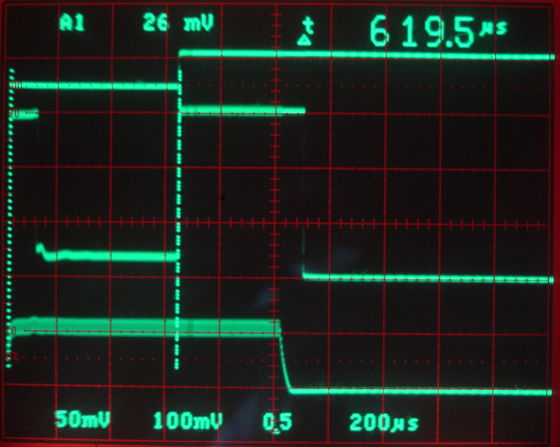
Figure: Power-Up From RF Pulse. Bottom trace is VR showing the 146-MHz on top of the demodulated signal, 500 mV/div. Middle trace is RP, 1 V/div. Top trace is OND, 5 V/div. Timebase is 200 μs/div.
The WK signal is asserted as soon as RP goes HI. After 110 μs, U10 powers up. While it configures itself, the RP input pin on U10 pulls RP down from 3.0 V to 0.38 V. Given that R21 = 50 kΩ, this observation suggests there is a pull-down resistor of 7.2 kΩ from RP to 0V during configuration. We re-program U10 with ONL asserted and a permanent pull-down resistor on the ONL output. Battery current increases by 100 μA, which suggests a pull-down resistance of 30 kΩ.
After 620 μs, U10 is configured. It asserts OND and turns off the pull-down resistors on all its inputs and outputs. The RP signal returns to 3.0 V until the end of the RF pulse. OND continues after the pulse, but goes LO after around 16 ms. The 1V2 supply relaxes to 0.8 V in 20 ms, steps down to 0.6 V in 5 ms, and relaxes to 0.4 V in the next 50 ms. The 3V0 supply relaxes only to 2.8 V in the same period. During the power supply relaxation, there are no spikes on OND. If we allow 10 s between pulses on RP, the power supplies relax almost to 0 V. Battery current returns to around 5 μA. We apply 1-ms pulses of RF at 100 Hz. Our P3030X02.vhd asserts OND continuously. Battery current is 250 μA.
We remove the oscillator instantiation from the code. We leave only the power controller, which we move into standby mode by asserting CLRFLAG briefly and then USERSTDBY permanently. Our new code is P3030X03.vhd. We apply 1-ms pulses of RF at 100 Hz. The power controller's STDBY output goes HI after four RCK periods. Quiescent current is 110 μA for VB = 3.3-4.2 V. We stop the pulses and battery current is 4.0 μA for the same range.
[21-AUG-14] The LCMXO2 is a CPLD (complex programmable logic device) constructed out of slices, where each slice contains two four-bit look-up tables (LUTs) and two outputs. Our firmware P3030X09.vhd implements a 64-byte command memory, a sixteen-bit cyclic redundancy check, a command processor, a stimulus generator, and a data clock running off a ring oscillator. The compiled logic uses 197 slices out of 640 available in the LCMXO2-1200. We remove three sixteen-bit registers and three sixteen-bit counters. The logic now uses 95 slices. It takes around 102 slices to implement 96 registered bits with accompanying combinatorial logic. The LC4256V, meanwhile, is a CPLD (complex programmable logic device) constructed out of macrocells, where each macrocell provides combinatorial logic and a single output. We use the LC4256V on the A3029A. When we remove 144 registered bits from the A3029A logic, the compiled code occupies 165 fewer macrocells. It looks like one slice in LCMX02 devices provides as much logic as one macrocell in LC4000 devices. But the FPGA provides in addition 8 KBytes of RAM and 8 KBytes of user-programmable ROM.
[22-AUG-14] Firmware P3030X09.vhd is now debugged and running, receiving commands, storing them in memory, reading them out, executing them, and generating lamp stimuli. We added modulation of the lamp power during each pulse. Compiled size of the code is 200 slices out of 640 available. We freeze this version now, and archive the jedec file here.
We expand the command memory from 64 bytes to 512 bytes, in anticipation of uploading EEG analysis algorithms to the central processor, which might be hundreds of bytes long. Compiled size for 9 address bits instead of 6 is 215 slices.
[15-JUN-15] Firmware P3030D01.vhd is now debugged and running. It provides random pulses with an average period equal to the interval length. In each interval, there are thirty-two instants at which a pulse can occur, each with an independent probability of 1/32. With a 2-s interval, we count 100 pulses in 207 s, for an average of 2.1 pluses/s. With a 100-ms interval and 10-ms pulses, we are able to count double-pulses, and we obtain an average of 9.3 pulses/s, with distribution shown below.

Figure: Distribution of Pulses per Second for Random 10-ms Pulses with 100-ms Interval. Average pulse rate is 9.3 pulses/s.
We may be under-counting pulses in the above experiment, because pulses that overlap by 50% we count as one pulse. The average pulse rate appears to be within 10% of the expected rate. We appear to have a decent approximation of a Poisson distribution for pulse occurrence. The spectrum of the pulses, as viewed in the Neuroarchiver, is shown here for a 32-s interval.
Micropower Oscillators
[07-AUG-14] One of the ISL technical challenges is generating a stable 5-MHz clock for an investment of less than 100 μA in quiescent current. In our Conceptual Design, we figured we could do this with the help of a Schmitt Trigger, a resistor, and a capacitor. The A3030 circuit provides two RC networks for use with the Schmitt Trigger inputs of U10.
We load R19 and R20 with 50 kΩ and C21 and C22 with 10 nF. The CKIN1 input to U10 is at R19/C21, while CKOUT1 charges C21 through R19. These are both 1.2-V logic, and it turns out that U10 does not provide hysteresis on 1.2-V signals. The CKIN2 input, on the other hand, is at R20/C22, while CKOUT2 charges C22 through R20. These are both 3.3-V logic, so we can program small or large hysteresis. We start with large. We set the output to the negation of the input for each clock.
We program the A3030X. Current consumption is now 6.1 mA when we assert OND with a jumper. The CK1 is running at some unstable frequency of order 20 MHz. We disable CK1. We have all kinds of problems re-programming the chip. We even replace U10. We remove CK1 from the firmware and we remove R19 and C21 from the board.
We are left with only CK2, and firmware P3030X04.vhd. We see the following traces on CKIN2 and on TP2 when we set it equal to CKIN2.
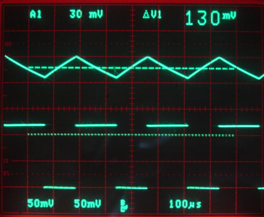
Figure: Clock Two for 50 kΩ and 10 nF. Bottom trace is CK2 as it appears in 1.2-V logic on TP2. Top trace is CKIN2. Both traces 500 mV/div and 100 μs/div.
We see the charging and discharging of C22 by R20. The average value of CKIN2 is 1.3 V. The hysteresis is 0.4 V. The clock frequency is 3.5 kHz, which is consistent with the 500-μs time constant of C22 and R20. Current consumption is 370 μA. When we remove R20, current consumption drops to 110 μA. The clock consumes 260 μA. If the current consumption were due only to R20 charging C22, we would expect only 30 μA.
We consult Understanding Schmitt Triggers. We reproduce Figure 1 below. The supply current of the SN74AUP1G14 micropower Schmitt Trigger inverter increases to 1 mA or 2 mA when the input is near the transition thresholds. We assume something similar happens at the inputs of U10 in our 3.5-kHz oscillator.
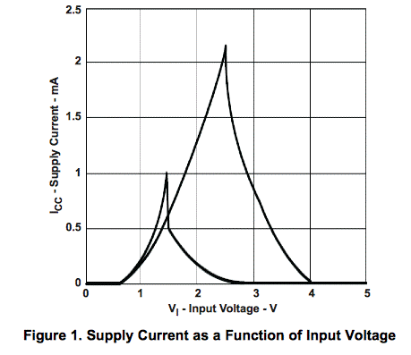
Figure: Current Consumption of Schmitt Trigger versus Input Voltage. Reproduced from Understanding Schmitt Triggers by Texas Instruments.
We try 100 kΩ/1 nF for R20/C22, but CK2 does not oscillate. We try 1 kΩ/1 nF and get 40 MHz and 2 mA total current. We remove both components and we are back to no oscillation and 110 μA total current. We try some other experiments, none of which are encouraging. We decide to abandon our plan to build a micropower RC oscillator. We remove CK2 from our firmware, leaving us with P3030X05.vhd as a starting point for future work.
[08-AUG-14] We build a ring oscillator using the BUFBA primitive, three gates in the ring, and divide by 64 to produce output on TP2. Our code is P3030X06.vhd. The ring oscillator powers up only when RP is asserted. We emit 5-ms pulses of RF every 20 ms, so the oscillator is running 25% of the time. The frequency of TP2 is a stable 1.2-V square wave of 2.37 MHz. The ring must be running at 152 MHz. Current consumption is 220 μA. Subtract the active quiescent current of 61 μA and multiply by four to get the ring oscillator current of 640 μA. This is only 4 μA/MHz.
[02-OCT-14] We add transmission scatter to the A3030B, but the ring oscillator is erratic. With fck_divisor = 17 the period of TCK is 170 ns, for 18 it is 240 ns. When we change the routing priorities of the ring oscillator gates, the ring oscillator won't turn off once it has turned on. The logic consumes 10 mA and and no data transmission takes place.
[03-OCT-14] The LCMXO2-1200ZE data sheet informs us that the delay through one LUT can be as high as 11 ns, and the maximum guaranteed clock frequency is 100 MHz. Given that our ring oscillator is running at 152 MHz, we are not surprised that the counter, which divides its frequency to 5 MHz, cannot keep up. We add two more gates to the ring oscillator and re-compile. We set fck_divisor to 10 and get TCK period 204.0 ns. The ring is running at 98 MHz. The figure below shows the ring oscillator gate connections within a cluster of four slices, where each slice contains two look-up tables. To obtain this compact arrangement of the ring oscillator, we set the routing priority of R1-R5 to 100.
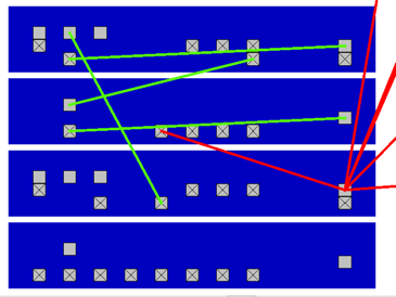
Figure: Placement of Five-Gate Ring Oscillator. Each blue rectangle contains two "LUTs" (look-up tables). The green lines are R1-R4. The red lines are R5, which distributes the ring oscillator clock to the transmit clock divisor gates. This ring runs at 98 MHz.
We obtain the following graph A of TCK period versus fck_divisor. Later we add further graphs to the same plot.
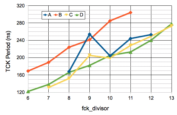
Figure: Variation of TCK Period with fck_divisor Value. We plot for various versions of the firmware. Version A uses a 5-gate ring and a 5-bit divider. Version B uses a 7-gate ring and a 4-bit divider. Version C uses a 5-gate ring and a 4-bit divider. Version D is also a 5-gate ring with 4-bit divider, but we have assigned a high routing priority to the 4-bit divider nets.
We try a larger ring oscillator, with seven gates, and we simplify the divider circuit, so that the divider is only four bits instead of five bits.
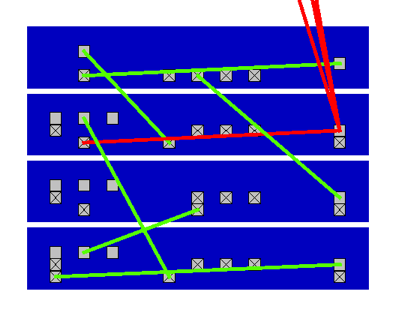
Figure: Placement of Seven-Gate Ring Oscillator. The green lines are R1, R2, R4, R5, R6, and R7. The red lines are R3, which distributes the clock to the four bits of the fast clock divider. This ring runs at 75 MHz.
The seven-gate ring runs at 75 MHz. We get linear increase in TCK period with fck_divisor, as graph B. But our TCK period resolution does not allow us to place the period within the range 195-218 ns required for reliable reception. We return to a five-gate ring, this time with the four-bit divider. The ring runs at 98 MHz again, and we get graph C. Our TCK period resolution is adequate, but we have an irregular period for fck_divisor = 9. The counter is failing to run at 98 MHz. We assign routing priority 75 to the four bits of the divider and re-compile. We obtain graph D, in which we see linear increase in period with divisor. Resolution is 21 ns, which is sufficient to guarantee that we can place the TCK period in the required range. We tell the compiler know that the ring runs at 100 MHz, TCK at 5 MHz, and RCK at 1.0 MHz and all timing violation warnings disappear. Furthermore, we now find that our quiescent current while transmitting at 512 SPS is 116 μA, which is 20 μA less than with our three-gate ring. Our firmware is now P3030B03.vhd and our parameter file is P3030A.lpf.
[24-OCT-14] We turn on the ring oscillator continuously by asserting OND in firmware P3030B03.vhd (we later correct the firmware so OND does not turn on the ring oscillator). Battery current is 1.25 mA, of which 130 μA is due to the logic chip and R22. We see 5 MHz on TP1. The ring oscillator consumes 1.1 mA, or 11 μA/MHz including the FCK and TCK dividers.
[02-JUL-15] In the P3030D02.vhd firmware, the ring oscillator is powered up only during lamp pulses. We measure the current consumption of A3030D No7 in various states: off 7.0 μA, stimulus outside a lamp pulse 59 μA, XON without stimulus 100 μA, XON and stimulus outside a lamp pulse 100 μA, lamp on (5V through 51 Ω and EZ500C470 is 45 mA) 74 mA.
[03-JUL-15] In the P3030D03.vhd firmware, we add a flag to disable transmission scatter, and a diagnostic transmit sample counter. With the use of the counter we confirm on the oscilloscope that No7 is transmitting 512 SPS. We eventually trace our 98% reception to problems with the mapping of the logic design into the chip. We must give all fast clock nets high routing priority. But each time we re-compile the code, there is a chance that the names of these secondary nets will be re-assigned. We must not allow the compiler to eliminate FCK or TCK from the design. When it eliminates TCK, it uses FCK and some clock enable lines to drive state machines, and this does not work. We force the ring oscillator and the fast clock divider into neighboring blocks in the chip. We now obtain 512 SPS from No7 and the ADC bits are reliable. We check frequency response to a sweep. With XON we get 100% reception of acknowledgments. But with XOFF we get 0% reception. We look at TXI and TXAD and U11-4. Whenever we issue a request for acknowledgment, we see the correct and expected pulse on these signals. And yet we do not receive an acknowledgment.
[04-JUL-15] It turns out that the MAX2624 oscillator needs time to stabilize before it transmits an acknowledgment. If it has been used within a few milliseconds to transmit another acknowledgment, or a data message, it's frequency will be correct during transmission. But if tens of milliseconds go by, it will need some tens of microseconds to stabilize. In P3030D04.vhd, we add a 30-μs warm-up before transmission and reception of occasional acknowledgments goes up to 90%. With 60-μs warm-up reception of one acknowledgment per second over three minutes is 100.0%. We check frequency response, data reception, command reception, and switching noise and all seems well. We create a clock divider entity and instruct the compiler to place all its nets in one contiguous block of eight slices. This means we no longer have to select the clock divider nets every time we modify the code.
[06-JUL-15] In P3030D04.vhd, we reduce the fast clock divider width from 5 bits to 4 bits. With the ring oscillator and fast clock divider locked in place, and high routing priority given to both functions, the maximum frequency of the clock divider has risen from around 110 MHz to 150 MHz, well above the likely frequency of our ring oscillator. We obtain the following graph of TCK period versus fck_divisor.
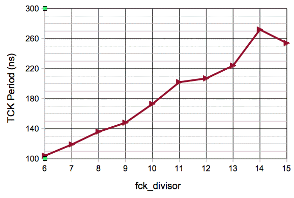
Figure: Variation of TCK Period with fck_divisor Value for A3030D.
For all values of divisor, the clock divider should be able to run at 150 MHz. The non-linearity of the above plot may be due to re-routing of the ring oscillator.
[09-JUL-15] We are still having trouble with the stability of the ring oscillator frequency as we re-compile with new values of fck_divisor. We add R5 to the ring and the router now places the five gates next to one another, so that the frequency is stable, as in P3030D05.vhd.
Data Transmission
The A3030A/B/C/D provided a single-ended amplifier that would act as a differential amplifier for EEG so long as the the lamp leads remained isolated from the animal body. With the lamp leads isolated, the X− lead anchors the ISL circuit to the animal body. The animal body charges and discharges the capacitance of the circuit with respect to the animal body, the impedance of which is negligible at EEG frequencies. But when the lamp leads connect to the body through an imperfect seal in the head fixture, this anchoring is compromised and lamp artifact appears in the EEG. The A3030E provides a differential amplifier and a 1.2-V terminal to act as a low-impedance anchor for the animal body, to be placed near the poing where the lamp leads exit the head fixture.
[26-SEP-14] We load the EEG amplifier and the RF oscillator on A3030A No1.1, making A3030B No1.1. We have firmware P3030B01.vhd. We have amplification of mains hum and transmission via 915-MHz data antenna. We can simultaneously turn on the lamp. We can turn on and off data transmission by command reception through the 146-MHz antenna. In order to stabilize the ring oscillator frequency as the oscillator is moved about the chip on successive compilations of the VHDL source code, we gave the three nets of the oscillator high routing priority, and as a result they are always place in adjacent LUTs. We still have a problem reading out the ADC: we appear to be getting bit 15 in place of bits 14 and 15.
[28-SEP-14] We fix a bug in the firmware and produce P3030B02.vhd. Our digitized X now looks correct. Its average value is 26780, which is consistent with our 1.2 V VCOM and our 3.0 V power supply to the ADC (1.2 / 3.0 × 65536 = 26214). We apply a 30-mVpp sinusoid with 20-MΩ source impedance to the X input and obtain the following plot of amplitude versus frequency.

Figure: Amplitude versus Frequency for 11-mV pp input on X. We see the bump in gain at around 130 Hz, which is a characteristic of our three-pole Chebyshev low-pass filter.
Ignoring C16, the input impedance at X is 12 MΩ, so we expect the amplitude of the signal at X to be 11 mVpp. The gain of the amplifier is nominally ×100 and the dynamic range is 3.0 V, so our nominal amplitude is 8500 counts rms or 24000 counts p-p. The frequency response for No1.1 lies within 1 dB of nominal.
Current consumption while transmitting X at 512 SPS is 137 μA. Of this, we know that 65 μA is not due to data transmission. Thus data transmission consumes 72 μA in this version of the firmware. We know that our ADC is active longer than it has to be, and the ring oscillator also. Both are active for an entire 30-μs period of RCK, when they are needed only for the 7 μs of actual data transmission.
[03-OCT-14] We implement transmission scatter in firmware P3030B03.vhd and slow down our ring oscillator from 150 MHz to 100 MHz. With fck_divisor = 10 we obtain TCK period 200 ns. Gain versus frequency remains within 1 dB of nominal. But battery current has dropped to 116 μA. Thus our data transmission consumes 51 μA in addition to the 65 μA quiescent current of the logic chip.
[02-JUL-15] In firmware P3030D02.vhd we have prompt acknowledgment, where the acknowledgment message is transmitted immediately the acknowledgment instruction is executed by the Command Processor. We instruct the A3030D to transmit 10 acknowledgments per second using our transmit loop script. We have the A3030D and the command and data antennas in a faraday enclosure. Over one minute we receive 98.7% of acknowledgments transmitted. We stop asking for acknowledgments and turn on the data transmitter. Over one minute, we receive an average of 99.6% of messages transmitted. We program the A3030D to transmit acknowledgments and data at 512 SPS. Over one minute, we see no change in the value of the acknowledgment messages, so we assume there is no corruption of the auxiliary data. We receive 98.5% of data messages and 98.0% of acknowledgments. Our transmit clock period is 218 ns with fck_divisor = 12. If we drop fck_divisor to 11, we get 190 ns. These values are on the extremes of our acceptable range for SCT messages.
[09-JUL-15] With firmware P3030D05.vhd, we obtain the following traces of TXADD (Transmit Acknowledgment Double Delayed), which marks the start of the 10-μs prompt acknowledgment transmission, and ILP (Initiate Lamp Pulse), which marks the start of the first lamp pulse of a stimulus cycle.

Figure: Prompt Acknowledgment to Lamp Pulse Delay. Top trace has a 60-μs pulse marking the moment the acknowledgement is transmitted. Bottom trace has a longer HI interval that marks the start of the first light pulse.
For the above trace, we have the interval length equal to 10 ms. The delay is 750 μs. When we increase the interval length to 100 ms, the delay is 6.3 ms. The bulk of the delay is the interval length multiplied by 2/33. But there will also be some multiple of 30 μs added, depending upon how the acknowledgment instruction is placed with respect to the start stimulus command. In the ISL Controller V4 with A3030Ds of ISL Stage 7 running P3030D05 firmware, the extra delay is five 30-μs clock cycles.
[10-JUL-15] While programming twelve A3030D for ISL7, we find that the ADC conversion fails when we get to D7.8, giving us X = 32768 counts with no input applied, and missing bits for a triangle wave. We put a probe on the CONV input and the conversion starts working. In P3030D05.vhd, CONV is combinatorial and can have a glitch on it 15 μs after it goes HI to initiate conversion. Depending upon how the design is mapped into the logic chip, this glitch may confuse the ADC or not. In P3030D06.vhd we fix the problem by making CONV synchronous, at the cost of a theoretical increase in current consumption of several microamps during data transmission. But we are left with some A3030Ds programmed with D05 and some with D06. We heat each to 60°C and cool to 0°C and they all work fine.
Battery Monitor
The A3030E reports its battery voltage when it receives a battery check instruction. The ISL Controller V5.2 provides automatic battery monitoring through the battery check command, and shuts off any device with battery voltage below 3.2 V, and gives a warning of low battery at less than 3.6 V, in accorance with our measurements here.
[19-JUL-17] The A3030E provides a battery voltage monitor by means of R26, R27, and Q2. When the device is in standby, the signal BT (battery test) from U1-43 is unasserted and Q2 is off. When active, the battery test command causes U10 to drive BT to 3.0 V, turning on Q2 and so connecting VB through R26 to R27. The voltage on R27 will be 3.3% of VB when R26 = 33 kΩ and R27 = 1.0 kΩ. We connect this voltage, VT (voltage test) to the CH1 input of U9, where we can digitize it with 46-μV precision, giving us 1.4-mV precision in measuring the battery voltage. Because the voltage divider is disabled except during measurement, the 100-μA current drawn by R26 will not add to our standby or operating current. We make R26 = 33 kΩ so that corruption of our battery measurement by corrosion between the terminals of R26 will be minimized.
[02-SEP-17] With the P3030E02 firmware we enable the battery power monitor by asserting the new BT output and selecting the second input channel on the ADC. Our E157.1 data transmission is now the digitized voltage on the R26/R27 divider. We multiply this by 34 to obtain the battery voltage. With the lamp off, the noise on the battery voltage measurement is 1.6 counts rms, or 1 μV and the battery voltage is 3.86 V. With the lamp on, we have noise 16 counts rms, or 7 μV and the battery voltage is 3.78 V. The spectrum of this new noise is flat from 0-255 Hz, but we see distinct positive spikes lasting one sample of height 70 μV. After 10 minutes, the battery voltage has dropped to 3.74 V with the continuous drain of the lamp.
[12-SEP-17] Firmware P3030E02 supports a check battery command, which we include in the latest ISL Controller. The battery command works only when data transmission is enabled. The A3030E responds with an auxiliary message with field address 2 (1 is for acknowledgement) and eight data bits that are bits 2-9 of the sixteen-bit ADC conversion. Their value is 127 for a 3.1-V battery and 157 for a 3.8-V battery. Our resolution is 23 mV in our measurement of battery voltage. We want to be able to detect when the voltage drops below 3.2 V.
[13-SEP-17] Firmware P3030E03 supports the battery check command even when the data transmission is not enabled. We measure the Battery Value (BV) in ADC counts versus applied battery voltage (VB) in Volts with a variable power supply and a voltmeter.
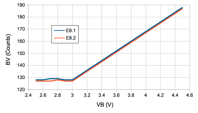
Figure: Battery Value (BV) versus Battery Voltage (VB).
The A3030E does not respond for VB <2.5 V. Its battery monitor we expect to be accurate only for VB > 3.0 V because only then is VB > VA = 3.0 V, the ADC's reference voltage. The slope of BV for both devices is exactly 40 counts/V. The offset between them is 1 count. We epect our accurracy in measuring VB with the above calibration of BV across all devices will be 25 mV rms.
Battery Recharging
[29-JUN-18] We provide instructions for recharging ISL batteries here, but we recommend that you do not attempt to recharge the devices yourself. After explantation the leads need to be checked for damage, and the recharging procedure is one that can easily go wrong. Send them back to us for recharge, test, and repair, using our ISL-RT and ISL-LR services. If we damage your device while recharging, we replace it with a new one.
The A3030E provides diodes D3 and D4, CMDSH2-3, which permit us to re-charge the battery through L+ and L−. We apply a positive voltage to the L− input and a negative voltage to L+ and recharge through the resistance of the lamp leads from the lamp pins.

Figure: Recharging Diodes. Diodes D3 and D4 conduct during charging.
[26-AUG-17] We apply an external power supply positive terminal to L− and negative terminal ot L+. Prior to connection, VB = 3.7 V. We apply 5 V and see 10 mA flowing into the battery, VB = 3.7 V. At 8 V we see 40 mA and VB = 3.8 V. Transmission of data continues uninterrupted. The circuit appears unaffected when we remove the charging supply. The forward voltage drop of the two charging diodes D3 and D4 should be around 0.24 V at 10 mA and 0.30 V at 40 mA. Assuming the battery voltage is constant, the lamp lead resistance is (8 − 0.6 − 5 + 0.48) V ÷ (40 − 10) mA = 96 Ω. When we apply 5 V and observe 10 mA flowing in, we deduce the battery voltage to be 5 − (0.01 × 96) − (0.24 × 2) = 3.6 V. Given that our current measurements are no better than ±5 mA, this 3.6 V is consistent with our measurement of 3.7 V.
[08-SEP-17] We find that our 190 mA-hr battery has run down after hundreds of thousands of flashes. We re-charge it through the A3030E lamp leads and continue work.
[12-SEP-17] Our 190 mA-hr LiPo battery has run down again. When it gets to around 3.2 V, the A3030E shuts down during lamp stimulus. Data transmission and stimulus stops. The device appears to return to its standby state, because we can re-start data transmission and attempt another lamp stimulus a few seconds later. The shut-down of the device on low battery is fortunate, because it will protect the battery from being over-drained while implanted.
[25-SEP-17] We observe corrosion of L− after a three-day soak in water with the device inactive, which we discuss in Lamp Pin Corrosion.
[13-OCT-17] We have E157.14 in quality control. We apply a voltage to its lamp pins and measure current flowing into the battery through the lead resistance and the charging diodes.
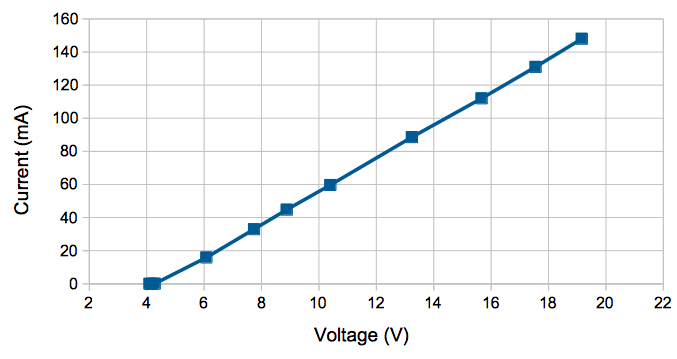
Figure: Charging Current versus Charging Voltage.
The slope of current versus voltage for voltages greater than 10 V implies a total lead resistance of 99.7 Ω. At 112 mA the forward voltage of our two CMDSH2-3 charging diodes in series is 0.70 V, the lead voltage is 11.2 V, and the applied voltage is 15.7 V, so battery voltage appears to be 3.8 V. But our ISL's battery monitor says 4.2 V.
[12-JUN-18] We discharge a battery by flashing the lamp for over 300 hours. We charge with 60 mA for 30 min. With a voltmeter we measure 3.71 V on the lamp leads. The reverse leakage current of the diodes is flowing through the 10-MΩ input impedance of the voltmeter. The battery monitor reports 3.8 V. We charge with 60 mA for another 60 min. We measure 3.81 V on leads and 3.9 V with monitor. After another 60 min we measure 3.91 V and monitor says 4.0 V. After another 45 minutes we measure 4.00 V and monitor 4.0 V.
[14-JAN-20] We have E157.8 back from ION not responding. Encapsulation puffed up with gas discharge from battery, but no odor discernable. Charge with 10 V across purple and orange leads for five minutes, now turns on and reports VB = 3.4 V. Transmits EEG. Responds to all commands at range 20 cm. Re-connect to charger. Current is 90 mA. Two hours later, 80 mA. Disconnect and device reports VB = 4.2 V.
[31-MAR-17] We place A3030D No12 in a beaker of water with the lamp leads outside the water but the EEG leads immersed. We turn on the data transmission and record for sixty seconds. The NDF archive of this recording is M1490986420. For the first twenty seconds we measure the noise in the amplifier.
Figure: EEG Amplifier Noise in A3030D. The EEG amplifier input impedance is 100 kΩ. The pass-pand of the amplifier is 0.3-160 Hz. The total noise in 0-256 Hz is 8 μV rms.
From 20-30 s we send repeated "transmit on" commands using our command transmitter. The command transmitter does not have its boost power connected, so it is transmitting around 1/5 W of 915 MHz command power. We see short gaps in the EEG recording, when the A3030D turns off its data transmission so as to avoid interfering with the incoming command. Other than that, we see no command power artifact. From 30-60 s we emit 10-ms full-power lamp pulses at 10 Hz. We see 160-μV negative-going pulses on the EEG signal.
[25-MAR-15] We place an un-encapsulated A3030C with firmware C01 on a data receiving antenna in a faraday enclosure. We flash the lamp at 10 Hz, 10-ms pulses, 100% brightness. But we do not connect the lamp. Nor do we have any EEG leads connected. The EEG input impedance is 10 MΩ. We have only a 10-mm two-pin connector on the lamp power output and our two 50-mm 915-MHz antennas. Input noise on X is 13 μV rms. We connect an LED on 50-Ω leads, so we expect 40 mA of lamp current. We see the following induced noise in the EEG input.
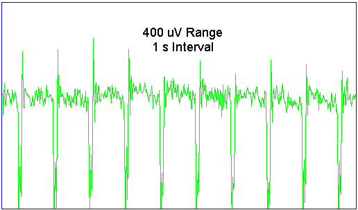
Figure: Lamp Current Noise on X for A3030C, Lamp Leads Running Away from Amplifier, No EEG Leads.
These negative peaks are 10 ms long and 200 μV high. In between the peaks, we have around 15 μV rms noise between the peaks. We curl the lamp power leads under the EEG amplifier and obtain the following traces.
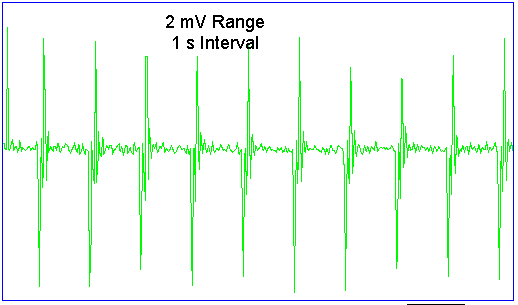
Figure: Lamp Current Noise on X for A3030C, Lamp Leads Looped Under Amplifier, No EEG Leads.
We replace our LED, power leads, and connector with a single 10-Ω resistor on the circuit board. We will now get 50-mA current pulses, and all noise we observe will be that which is exchanged within the circuit board.
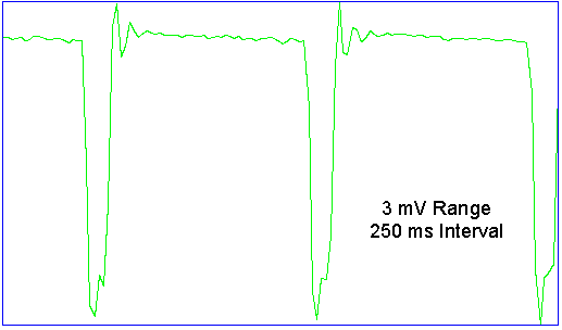
Figure: Lamp Current Noise on X for A3030C, No Lamp Leads or Connector, 10-Ω Resistor Load.
We examine the circuit voltages with an oscilloscope. Outside the 10-ms pulses, VBAT is 4.0 V. As soon as the pulse begins, VBAT drops to 3.6 V. We are supplying power through the programming extension. On the circuit board, 0 V jumps up by 20 mV compared to 0 V on the programming extension. We believe this is due to the resistance of th 5-mil trace that leads from the programming extension. We solder a battery directly to the circuit board. This battery's voltage drops from 3.9 V to 3.7 V when we turn on the lamp and we no longer have any jump in 0V. The noise induced by the current pulses remains as shown above.
We examine VA, which powers the EEG amplifier. We see 10 mVpp of a 512-Hz triangle wave, which vanishes when we turn off data transmission. We solder the X inputs together. The pulses remain 3 mV high. We replace C8 with 33 kΩ. The pulses drop to 400 μV.
[27-MAR-15] We load 10 kΩ for R5 and R6, 100 kΩ for C15. Our input impedance is now 120 kΩ. We generate 10-ms pulses at 10 Hz into our 10-Ω load. We get the following EEG interference.
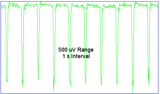
Figure: Lamp Current Noise on X for A3030C, 10-Ω Resistor Load Soldered to Board, 120 kΩ Input Impedance.
We load toroidal inductor 83103C for L2, thinking it will generate less stray magnetic field. We obtain the following interference.
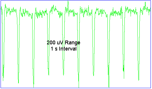
Figure: Lamp Current Noise on X for A3030C, 10-Ω Resistor Load Soldered to Board, 120 kΩ Input Impedance, Toroidal Inductor for L2.
The toroidal inductor reduces the amplitude of the interference spikes by a factor of 2.5, but as we found earlier, the efficiency of the boost converter drops from 89% to 76% with this inductor. That's why we removed the toroidal inductor footprint from the A3030C circuit boards. But we can still load it on the board with the help of a wire.
[10-APR-15] We have A3030C No6.1 programmed with P3030C01.abl firmware, which turns off the boost converter for each pulse, rather than leaving ENL asserted throughout a stimulus. We have restored the non-toroidal inductor. We have two antennas loaded. We have R5 = R6 = 10 kΩ, C16 = 10 μF, R7 = 100 kΩ. Thus we have AC-coupling on the input with 1-s time constant as before. Gain versus frequency with 50-Ω source is correct. We have joined-pair 100-mm lamp leads and 150-mm electrode leads soldered in place. We flash a white LED for 50 ms every 200 ms and see the noise below.
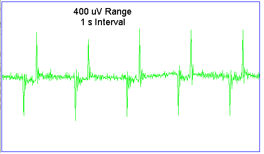
Figure: Lamp Current Noise on X for A3030C with Paired Leads, White LED, 120 kΩ Input Impedance.
[07-MAY-15] Our ISL6 A3030C devices have 120 kΩ input impedance with a 10-μF capacitor for a high-pass filter. The lamp leads are stuck together with silicone, as are the electrode leads. The command antenna is shorter. We turn off the boost regulator between pulses. We place C6.1 in water with the lamp lead ends above the water surface and no lamp attached, so there is no lamp current flowing.
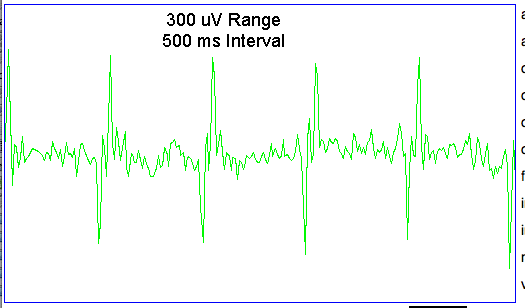
Figure: Lamp Voltage Noise on X for A3030C with Lamp Pins Above Water. Pulses of 10 ms every 100 ms.
We attach a white LED outside the water so lamp current pulses are now flowing down the lamp leads.
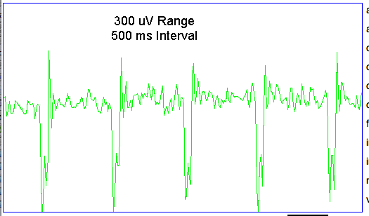
Figure: Lamp Current and Voltage Noise on X for A3030C with Lamp Pins Above Water and White LED Attached. Pulses of 10 ms every 100 ms.
When we immerse the lamp leads in water, we get full-scale transitions on the EEG input. We keep the lamp contacts outside the water, but run the lamp and EEG leads as close as we can underwater. We get the following noise.
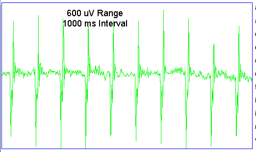
Figure: Lamp Current and Voltage Noise on X for A3030C with Lamp Pins Above Water, White LED Attached, and Lamp and EEG Leads Running Close Together. Pulses of 10 ms every 100 ms.
We increase the pulse length so we can see noise between the pulse edges.

Figure: Lamp Current and Voltage Noise on X for A3030C with Lamp Pins Above Water, White LED Attached, and Lamp and EEG Leads Running Close Together. Pulses of 100 ms every 200 ms.
We cover the white LED to make sure none of its light can affect the EEG input by some photovoltaic effect. The noise remains as shown above. We conclude that electrical isolation between the lamp and EEG contacts is essential for reducing the lamp noise.
[19-MAY-15] We place C6.4 in a faraday enclosure with a data and command antenna. We enable data transmission and watch the X signal in the Receiver Instruments. We transmit stimulate commands to channel 8, which C6.4 examines and ignores. When we transmit the command, we see a step up in X of 1.7 mV followed by an exponential decay with time constant 0.3 s.
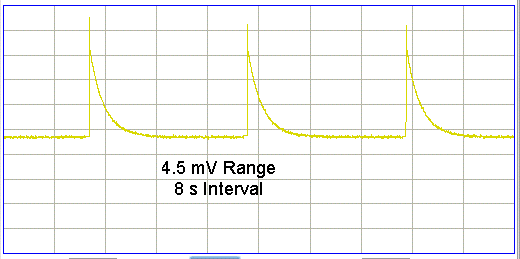
Figure: Command Reception Noise on X for A3030C with A3029B emitting 30 dBm of 915 MHz.
We disconnect boost power from the A3029B so that output power drops to around 20 dBm and the step size decreases to 270 μV. We instruct C6.4 to generate 50-ms pulses of 100% brightness at 10 Hz, but we have no lamp connected. We see no sign of the lamp switching in X. We switch to 20% brightness and get the modulation noise shown below.

Figure: Lamp Modulation Noise on X for A3030C with 20% Brightness, 50-ms Pulses at 10 Hz, no LED attached, no X leads.
The above noise is exactly the same for 20%, 40%, 60%, and 80% brightness.
[24-JUN-15] We obtain the trace below of random pulse modulation noise from the A3030D with Q1=NTR4003N and 80% modulation, 10-ms pulses at 10 Hz average frequency.

Figure: Lamp Modulation Noise on X for A3030D with 80% Brightness, 10-ms Random Pulses at Average 10 Hz. No X leads. No LED.
Each graduation in the image is 30 counts, so the modulation noise is of order 100 counts, which corresponds to 46 μVpp.
[26-JUN-15] We turn on data transmission in No7.7, and A3030D with both antennas, no lamp leads, and 100-mm X leads. We send a Stimulus Stop command with 30 dBm of command frequency power 20 cm from the A3030D and observe the following step in X.
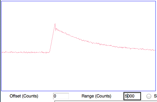
Figure: Radio Frequency Power Noise, 30 dBm at 20 cm. The step is around 600 μV high. For the same plot at 22 dBm at 20 cm, see here.
At range 40 cm the step is only 100 μV. When we send a Stimulus Start command, the step is the same size in both cases, except it is followed by pulses of lamp noise. Out lamp is a 50-Ω resistor in series with an EZ500C460 loaded on the circuit board and covered with epoxy. The lamp current is around 44 mA. We now see the noise resulting from lamp current. Regardless of how we arrange the two X leads, these pulses remain 200 μVpp. We examine the battery voltage during the pulses and see an initial 60-mV drop for 10 μs followed by 200 kHz noise from the boost regulator, with an average drop of 30 mV below the normal battery voltage.
[26-AUG-17] The A3030E is equipped with a differential amplifier and the boost converter is better isolated between the battery tab connections than in earlier layouts. The result is dramatically reduced electronic lamp artifact.
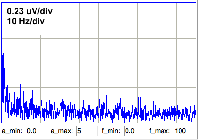

Figure: A3030E Lamp Artifact in Air. Left: No Flashing. Right: Flashing at 100% Brightness. We have a white LED on the end of 150-mm stretched leads. Flashing at 10 Hz, 10 ms flashes. The vertical scale is 0.5 counts per division, or 230 nV/div. The fundamental of the lamp artifact is at 10 Hz with amplitude 2 μV.
We reduce brightness to 20%, so that lamp current is modulated at 1 MHz by Q1. With the EEG leads far from the lamp leads, we see negative pulses of 300 μV during lamp pulses. With EEG leads running next to lamp leads, we see negative pulses of 3 mV. If we disconnect the tips of the lamp leads we see positive pulses of 10 mV. We move the leads and we get negative pulses of 10 mV. The X signal at U13-4 shows −20-mV pulses. We twist the leads together and pulses are less than 100 μV.
[29-AUG-17] We flash the D8.1 lamp at power 0% up to 100% and measure the modulation artifact picked up by the EEG leads. We try various modifications to eliminate the artifact.
Figure: Amplitude of Fundamental Component of Modulation Artifact. The modulation is 50 ms pulses at 10 Hz with varying brightness. We try with and without 150-mm EEG leads, with capacitors across the base of the leads, open circuit and short circuit at the ends of the leads. When we have leads, we arrange them in the same way every time.
The artifact is not magnetic, or else it would stop when we disconnect the ends of the leads. It is not differential, or else it would disappear when we connected 10 μF across the base of the leads. We cannot eliminate it by placing 100 pF across R19 and R20. The noise is common-mode. It is reception of the 1 MHz power radiated by the lamp leads. This noise cannot be rejected by U13 because its gain is insufficient at 1 MHz. Non-linearity in U13 demodulates the 1 MHz so as to generate the 100-Hz artifact. We connect 100 pF from X+ to X−, and 100 pF from X− to 0V. Better would be to connect both to 0V but we see no easy way to connect a capacitor directly from X+ to 0V. These capacitors act as 1.7 kΩ resistors at 1 MHz, and so carry the common-mode power away to ground. They reduce the artifact to below 20 μV. The source impedance of the 1-MHz common mode noise is of order 1 MΩ. When we manipulate the leads into new positions, we cannot increase the artifact to more than a few hundred microvolts.
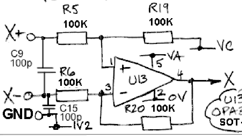
Figure: The Differential Amplifier, Equipped with Decoupling Capacitors C9 and C15.
We apply a 1 Vpp sinusoid to X+ and X− with respect to the circuit 0 V. The common mode voltage range for the U13 amplifier is −1.2 V to +6 V, so our ±0.5 V input is well within range. We measure the rms amplitude of X in ADC counts and multiply by 1.3 μVpp/count to get the differential input that would give the same sinusoid on X.
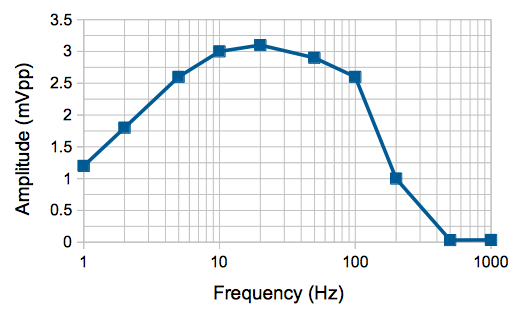
Figure: Apparent Differential Input Generated by 1 Vpp Common-Mode Sinusoid on X.
The common mode rejection ratio is around 350 in the center of the amplifier's pass-band. This is consistent with the resistors R5, R6, R19, and R20 being ±1%. If we were to use 0.1% resistors we may get better common mode rejection. We measure the differential gain also, applying a 30 mVpp sinusoidal sweep to X. We connect X− to the A3030E 0V and the 0V of the incoming sinusoid.
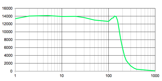
Figure: Output Amplitude (counts rms) versus Frequency (Hz) for 30-mVpp Differential Input.
The differential gain appears is undisturbed by the presence of the two 100 pF capacitors connecting the X inputs to 0V. At 100 Hz, the impedance of 100 pF is 17 MΩ, which is much greater than the 200-kΩ differential input impedance of the U13 amplifier. We add the two 100 pF capacitors as C9 and C15 to the schematic.
Sources of Lamp Artifact
[20-JUL-17] As revealed in the account below, the silicone insulation of the lamp leads does not adhere to the dental cement of the head fixture, so that the leads slide in the tunnels that carry them through the dental cement to the fiber-coupled LED. The following diagram shows how the conductivity of the tunnel creates lamp artifact of hundreds of millivolts when the ISL records EEG while the lamp is flashing.
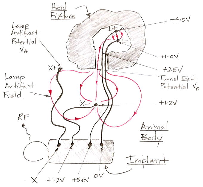
Figure: Lamp Artifact Current Flowing From L+ to X− When Lamp Is On. Voltages with respect to the implanted A3030D's 0V supply. Head fixture made of dental cement.
Current flows through a film of body fluid from L+ to L−. Our calculations suggest that the resistance of the body fluid between these two terminals is around 1 kΩ. Current flows from within the head fixture, through the lamp lead tunnels, to X−, which is connected to 1.2 V within the implant. The voltage at the entrance to the tunnel is VH ≈ 2.5 V. The resistance of the tunnel, RT, can be as low as 100 kΩ. The resistance, RB, from the tunnel to X− through the animal body can be as high as 10 kΩ. The voltage at the exit from the tunnel is:
VE = 1.2 V + (VH − 1.2 V) RB
/ (RB + RT)
Inserting 100 kΩ for RT and 10 kΩ for RB we get VE = 1.32 V, which is 120 mV above X−. The potential VA at X+ will be somewhere between 1.20 V and 1.32 V. Our biopotential measurement is X = VA − 1.2 V = 0-120 mV. With the field lines as they are drawn, and assuming uniform resistivity in the animal body, X will be something like 100 mV. When we turn the lamp off, the L+ and L− terminals are disconnected from the implant circuit. The current flowing from L+ to X− stops. The electric field vanishes. In the absence of any biometric signal, X = 0 mV. Thus X jumps up by 100 mV when we turn on the lamp. This is the lamp artifact. The artifact decreases with tunnel resistance and increases with body resistance.
In the section below, we describe our observation and identification of the tunnel-conduction lamp artifact in the ISL's EEG input. In Lead Sealing we describe our efforts to eliminate this artifact by increasing the tunnel resistance to >10 MΩ using water-tight collars around the lamp leads where they pass through the dental cement. Our dual-bore ceramic collar was effective, but we remain uncertain of its reliability in a long-term implant.
Another way to eliminate lamp artifact is to abandon the ISL EEG input and implant a separate A3028E SCT to monitor EEG. In such an arrangement, the ISL makes electrical contact with the animal only in the head fixture. No lamp current flows through the animal body because there is no way for such current to re-enter the ISL circuit other than through L−, which is within the head fixture.

Figure: Separate SCT for EEG, ISL without EEG for Lamp. Head fixture made of dental cement.
The SCT's X− input is connected to the SCT 1.8 V power supply. The body charges the SCT's body capacitance so as to keep the SCT's 1.8 V potential at the same potential as the body, VB in the diagram. The body capacitance of the A3028E is of order 100 pF. At 160 Hz, the upper end of the A3028E bandwidth, 100 pF has impedance 10 MΩ. If the X− electrode is a wire held by a skull screw, its impedance is around 1 kΩ, so it has no trouble charging the transmitter body capacitance. We demonstrate how well this arrangement eliminates lamp artifact in Separate EEG Monitor.
In the following arrangement, we add a grounding lead from the ISL to a grounding spring that winds around the lamp leads where they pass through the dental cement of the head fixture. We make no attempt to seal the tunnel through the cement with a collar, but instead absorb the lamp artifact current with the grounding spring.

Figure: Grounded Seal Arrangement. Head fixture made of dental cement.
Current from L+ traveling along the water on the surface of the silicone leads passes into the grounding spring, which is at 1.2 V with respect to the ISL circuit. Current flows from the grounding spring to L− also. But no current flows into or out of the animal body to the lamp leads or the grounding spring, other than the current needed to charge the ISL body capacitance of order 100 pF. In the absence of biopotentials, the animal body potential is the same as the 1.2V potential in the ISL circuit. We have VB = 1.2V = GND = ground potential.
In theory, we could now connect X− to 1.2V inside the ISL as well, and so use a single-ended amplifier to obtain the difference in potential between X+ and X−. But it is possible that the connection between the grounding spring and the tunnel fluid will be imperfect, so that some current will leak out and travel in a small circuit near the edge of the head fixture. If we connected X− directly to 1.2V, some of this leaking current will flow through the animal body to X−, but not to X+, which is the high-impedance input of our amplifier. The result would be lamp artifact on X+, although a much smaller artifact than without the grounding spring.
Because the ISL potential is already anchored to the animal body potential by the grounding spring, we do not need to anchor the ISL to the body with a low-impedance ground at X−. We can instead connect X− and X+ to the inputs of a differential amplifier of sufficiently high input resistance that neither input will attract lamp current. An input impedance of 200 kΩ as shown here should be sufficient, but not so large as to invite the electronic noise we describe above.
By the above arrangement, we hope to eliminate lamp artifact without a collar seal. The ground spring should be a snug fit around the two lamp leads, but we can slide it up the leads during implantation, so one end is close to the L+ and L− pins and the other end protrudes from the head fixture cement. Upon explantation, we dissolve the dental cement in acetone and recover the entire apparatus, ready to re-charge the battery through the lamp leads. We describe our work on this arrangement in Tunnel Grounding
Observations of Lamp Artifact
[22-SEP-15] We have A3030D number D7.2 implanted at ION since 17-AUG-15. The day after implantation we observe full-scale artifacts on the EEG when transmitting commands, and the following 15-mVpp pulses when flashing the lamp.

Figure: Lamp Flashing Artifact for First A3030D Implanted, D7.2. Archive M1439901477.ndf, 2352 s.
Last week we observed only the 200-μVpp artifact we expect from our tests at OSI. We consider the possibility that dental cement (acrylic and powder) mixed with water is conducting until the water evaporates. We mix up dental cement with and without adding a few drops of water. When we add water, we get drops of water coalescing outside the cement. (Methyl methacrylate is hydrophobic.) Resistance between two probes placed 0.5 mm apart is greater than 10 MΩ in all cases. We cement two wires 5 mm apart and plug the electrodes of a 10-MΩ amplifier into the cement near each wire, but not in contact with the wire.

Figure: Cement Noise Coupling Measurement. We use an A3028E with 10-MΩ input impedance to pick up a 5-V square wave applied to two wires embedded in the cement.
We bake our apparatus at 60°C to make sure it is dry. We apply a 5-V, 10-Hz square wave to the two wires and observe the following on the A3028E output.

Figure: Cement Voltage Coupling. We have 10-MΩ input impedance and a 5-V, 10-Hz square wave applied to the wires.
We cover both amplifier electrodes with a few drops of water. The impedance between the electrodes is now 600 kΩ measured at 0 Hz. The coupled signal drops to less than 100 μVpp from 10 mVpp. We dry off, apply a 5-Vpp sinusoid, and obtain the following graph of coupled amplitude versus frequency. The slope of the graph suggests the coupling through the cement is capacitive.

Figure: Cement Voltage Coupling versus Frequency. The initial positive slope shows coupling increasing as f. After 160 Hz, the attenuation of the three-pole low-pass filter changes the response to 1/f2.
At 100 Hz, we get 0.1% of the applied sine wave at our amplifier input, which suggests that our 10-MΩ input impedance is 0.1% of the impedance of the coupling capacitance, so that this capacitance is of order 0.2 pF. The dielectric constant of this cement should be around 4, so 0.2 pF can be made with two 2-mm square plates separated by 1 mm. We cut the blue X− lead. The coupled noise remains the same. We cut the X+ lead. The noise drops from 10 mVpp to 100 μVpp.
Our cement does not conduct electricity, even when we add water during mixing. The input impedance of the A3030D amplifier is 100 kΩ. If both electrodes are connected to the brain, the impedance between them will be closer to 1 kΩ. In either case, the noise coupled from a 5-V square wave applied to the same lump of dental cement will be less than 100 μV. Even if we disconnect the X− and leave X attached, artifact will be less than 100 μV.
Conduction through dry or wet cement cannot explain the artifact we observed from D7.2 when it was first implanted. Capacitive coupling cannot explain the artifact either, because the A3030D has input impedance only 100 KΩ.
[12-NOV-15] At ION, we have D7.6 implanted. We record full-scale lamp stimulus artifact in the EEG input. With 0% brightness, 10 ms pulses, 100 ms period, we get these full-scale square waves at 10 Hz (see M1447342849.ndf). We watch the implantation of D7.5 and note the L+ and X leads are touching before we apply dental cement. We believe the previous two implants were done exactly the same way, so L+ and X were touching. This time, we move the leads apart before we apply dental cement. If they were to touch, there would be a passage through the dental cement for water to creep along and so connect X to L+. Half an hour after implantation, we generate 0% brightness, 10 ms pulses, 100 ms period and see the pulses below.

Figure: Lamp Pulse Artifact Immediately After Implantation. D7.5, 0% brightness, 10-ms pulses, 100 ms period.
We see a step up on X as the lamp power turns on. Brightness is 0%, so L− is open-circuit and L+ is connected to +5V. When we turn off lamp power, L+ relaxes as C13 discharges. At no time is Q1 turned on.

Figure: Lamp Pulse Artifact Immediately After Implantation. D7.5, 100% brightness, 10-ms pulses, 100 ms period.
With 100% brightness, the artifact on X has a sharp fall as well (see M1447350049.ndf). In this case, L+ drops quickly at the end of a pulse because L− is connected to 0V for 200 ns after the end of the pulse. The artifact on X is 15 mV for a 5-V change in L+. The X input is connected to VCOM by 100 kΩ inside the ISL and by roughly 1 kΩ through the brain of the animal. The artifact is consistent with a resistive connection between L+ and X of 5 V ÷ 15 mV × 1 kΩ = 300 kΩ. We take two silicone-insulated steel leads and solder them to the pins of a connector. We glue cover the connector with cement, but leave the solder joints exposed. We put saltwater on the joints. We tie the two leads in a knot to make sure they are touching. We cover the leads and joints with cement. The resistance between the two leads is >40 MΩ. We allow the cement to cure. We cover with salt water. At first, resistance remains >40 MΩ. But after half an hour, it has dropped to 120 kΩ. We pour away the saltwater and dry the cement, resistance is 100 kΩ. After an hour, it remains the same. We bake in the oven at 60°C for half an hour, resistance is 130 kΩ. After one hour, it is >40 MΩ
[17-NOV-15] It is water traveling by capillary action along the surface of the silicone insulation of the lamp leads that is bringing out of the head fixture the lamp power voltage. We present our experiment and results in Conduction Through Tunnels.

Figure: 100-kΩ Liquid Tunnel Resistor. The resistor is provided by the film of water around the knotted silicone leads in the dental cement.
In the photograph above, the ends of the red and blue leads, outside the dental cement, are connected by 100 kΩ, even with the surroundings dry. After half an hour drying in the oven at 60°C, the resistance is still 130 kΩ. Another hour later, the resistance is >40 MΩ.
Lead Sealing
[11-DEC-15] Following our discovery of conduction through tunnels, we perform the following experiment to test if we can, during implantation, seal the ends of the lamp leads with silicone. We make a head fixture with no guide cannula or fiber. We seal the LED with clear epoxy. We hold the fixture with the LED downwards and connect the leads of our D7.7 ISL, like this. We apply MED10-6607 silicone dispersion until it almost drips off the underside, see here. We allow the silicone to cure. After ten minutes it looks like this. After twenty, as below.

Figure: Silicone Around Lamp Leads, Twenty Minutes After Application.
We apply dental cement, allowing it to run off the underside. We start with thin cement, then thicken and make sure we cover the top side. The result is shown below. We note an obvious tunnel into the cement between the two lamp leads.

Figure: First Coat of Dental Cement over Head Fixture.
We allow the cement to cure for twenty minutes. We note that the pads around the LED are still exposed on the bottom side. We place the ISL and head fixture in water and observe full-scale lamp artifact. We surround the entire fixture with cement.

Figure: Encapsulating Coat of Dental Cement.
We let the above cement cure for ten minutes, then we place the ISL and head fixture in water. We get the following lamp artifact after one minute.

Figure: Lamp Noise Just After Dropping in Water.
We put hot water in the beaker. We take out the ISL and flex its lamp leads twenty or thirty times. We put the ISL and head fixture back in the water and let it settle down. We see the artifact below.

Figure: Lamp Noise 20 Minutes After Dropping in Water.
We move the EEG leads out of the water and record noise. We get this, which is pretty much the same as with the leads in the water. We wrap the lamp leads around in a loop with the EEG leads and put everything in the hot water. No change to the noise. We wait one hour to give capillary action time to move water into the dental cement.


Figure: Lamp Noise One Hour After Dropping in Hot Water. Range 800 μV, Interval 1 s, Pulses 50 ms, Pulse Period 500 ms. From top-left to bottom right: Lamp stimulus off, stimulus with 0% brightness, 20%, 40%, 60%, 80%, 100%, 100% with EEG leads out of water.
We see the artifact reversing direction as we increase the lamp current. If we re-arrange the leads, the artifact changes.

Figure: Lamp Noise for 100% Brightness After Rearranging Leads. Range 800 μV, Interval 1 s, Pulses 50 ms, Pulse Period 500 ms.
We now encapsulate the EEG leads with dental cement. When we immerse in water, the artifact remains much the same. It appears that our silicone sealing of the lamp leads has increased the resistance between the lamp power terminals and the water in the beaker.
[14-DEC-15] After 72 hours in water, we measure artifact again with 50 ms 100% pulses.

Figure: Lamp Noise for 100% Brightness After 72 Hours Soaking.
With the lamp out of the water, the noise drops back to hundreds of microvolts, and with the EEG leads out of water as well.
[15-DEC-15] After a one-hour dry bake at 60°C, lamp noise for 100% brightness in water has dropped back to normal amplitude. We prepare another head fixture and cover all electrical pads on its top and bottom surfaces with clear DB270 epoxy, see below.

Figure: Epoxy Sealing of Head Fixture Conducting Surfaces.
We have coated both sides, but stayed clear of the two sockets. We used a thin wire to apply epoxy between the sockets and the LED footprint. We cut the existing head fixture and cemented pins off D7.7 and solder new pins to the lamp leads. We strip and tin the EEG leads.
[18-DEC-15] We connect lamp leads to the head fixture shown above and flash the light. We cover the pins and sockets with silicone. We wait twenty minutes, with the silicone curing above a bath of warm water. We touch the silicone with tweezers and note that it is not yet tack-free. If we were to apply dental cement, we would disturb and compromise the silicone coating. After one hour, it is tack-free. We lower the entire assembly and ISL and EEG leads into water and observe lamp full-scale lamp noise. We put the lamp in our mouth and cannot taste the signal, which means it must be less than 500 mV. So we suspect we are seeing lamp noise on the EEG of order 100 mV. We feel sharp edges around the corners of the circuit board. The silicone is discolored, because it has not had sufficient time to cure. We conclude that applying one coat of silicone during surgery is not sufficient to seal the lamp power electrodes.
We move on to our Insulating Collar idea. Our objective is to stop water propagating along the outside of our silicone lamp leads and reaching the metal of the electrodes. We propose to put a collar around each lamp leads that is non-conducting, but which the dental cement bonds to securely. With contact between the dement and the collar, and the collar and the silicone, we would divide the water film into two parts, one in contact with the lamp power pins, the other in contact with the rest of the body.

Figure: Cross-Section of Insulating Collar. The water film around the silicone leads is interrupted by the insulating collar. The dental cement binds directly to the collar.
We try heat shrink tubing as a collar. The smallest diameter we have is 2.5 mm on the outside before we shrink it, and roughly 0.7 mm on the inside after we shrink it. Our lamp leads are 0.9-1.2 mm in diameter. When we shrink the tubing onto one of these leads, we can slide the collar up and down the lead afterwards by stretching the lead so as to reduce its diameter. We need a narrower diameter tubing or we need a way to glue the tubing to the silicone. Setting that problem aside for now, we put some tubing in dental cement to see if we get good wetting of the plastic surface by the cement.
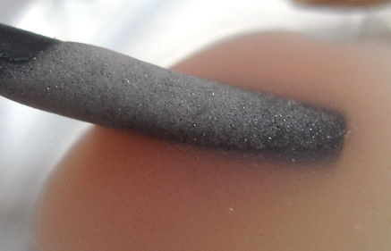
Figure: Adherence of Dental Cement (Acrylic) to Heat Shrink Tubing.
When we try to pull the tubing out of the cement, it breaks at the top surface of the glue, leaving the rest inside. We put collars on two silicone leads. The leads have bare spring terminations. We glue the collars into dental cement, as shown below. Because of the collars, the two leads become separated by a layer of dental cement, which surrounds the collars by capillary action of the acrylic. Resistance between the two leads is >40 MΩ. We put the ISL with head fixture, and the two-wire apparatus, in salt water for the weekend.

Figure: Collars Glued Into Dental Cement.
When the cement has hardened, we put the cup and leads in water at 60°C for half an hour, to allow water to penetrate wherever it can by capillary action. Resistance is >40 MΩ. We put the beaker on our bench and measure the resistance as time goes by. Fifty minutes after first contact with water, the wires are still insulated from one another. We add salt. Resistance between two pins 1 cm apart is now less than 1 kΩ. With the cement still in salt water, we hold it in place and pull on the two leads one hundred times. Insulation is intact. After another ten minutes, insulation is still intact.
We pull the silicone off our epoxy-sealed head fixture. We cut back the lamp leads on D7.7 and attach another set of pins. We add a collar to each lead, connect the pins to the head fixture, and encapsulate in dental cement. Once the cement is hardened, we break the cement out of its red plastic cup. We immerse in hot water, see here. We pull on the lamp leads 100 times. Lamp artifact with 100% brightness is a few hundred microvolts, and consistent with no conduction between the lamp leads and the EEG leads.
Two hours later, we see 10-mV lamp artifact on the EEG input of the ISL, but we still have isolation between the two test leads in dental cement.
[22-DEC-15] We see full-scale lamp artifact on our D7.7 input after soaking for four days in saltwater. We cut the LED fixture from the leads and measure 5 MΩ impedance between the two wires through the head fixture in both directions. The impedance of a bare, blue LED is ∞ according to the same ohmmeter in both directions. We dry the head fixture in the oven for half an hour and the impedance rises to ∞. We attach our separate two-wire fixture to the lamp leads. We keep the metal joints out of water, but immerse the fixture and EEG leads. We see full-scale artifact. When we remove the two-wire fixture, we measure ∞ Ω between the wires. We immerse the fixture in water. The resistance between the blue wire and the water is ∞ Ω, but between the red wire and the water is 10 MΩ.
We have a Loctite Super-Glue Gel, which is reputed to be able to glue silicone. We put 3-mm long collars on two wires that are terminated with screws, shrink the collars, and slide them onto a portion of wire coated with the glue gel. We put three 1-mm long collars on two red wires terminated with bare springs, as shown below. With the help of tweezers, we manage to glue all of them to the silicone.

Figure: Triple-Collars, modeled after the triple o-ring seals we see in pacemaker connections.
Once the gel has cured, we can no longer slide the collars along the silicone. We embed the collars and wire tips in dental cement. When cured, we immerse in saltwater and arrange the free ends of the wires so we can measure easily the resistance between each wire and the water. We pull on all four leads one hundred times each with a force of sufficient to stretch them by 15% while they are wet with saltwater. We leave them for one hour. We combine a 10-V power supply with our 10-MΩ millivoltmeter to make an instrument capable of measuring resistance up to 100 GΩ. The water connection resistance is 20 GΩ for the two triple-collar red leads and >100 GΩ for the single-collar blue leads.
[23-DEC-15] Water connection resistances today are 100 GΩ, 30 GΩ, >100 GΩ and >100 GΩ for red left, red right, blue left, and blue right. If we want 5-V lamp power artifact to be less than 500 μV at our 100 kΩ input impedance, the water connection resistance must be greater than 1 GΩ.
[24-DEC-15] Water connection resistances today are 100 GΩ, >100 GΩ, >100 GΩ, and >100 GΩ for red left, red right, blue left, and blue right. We connect the two red leads to D7.7's lamp power, with a blue LED in parallel. The blue LED flashes. We lower the ISL into a beaker of water with the cement fixture. We see 500 μV artifact. We do the same with the two blue leads, but connect no LED. We obtain 500 μV artifact.
We pull 100 times on each of the two blue leads with a peak force sufficient to extend them by 30%. Both are wet with saltwater. We put the cement fixtures back in the saltwater with the ISL and observe the full-scale artifact below.

Figure: Artifact After Breaking Single-Collar Seals with 1-N Tugging.
We have broken the seal. We do the same with the pair of triple-collar red leads, applying a force sufficient to stretch the leads by 30%, tugging 100 times. When we are done, the leads curl up because we have deformed the springs. We put the fixture back in the water and observe the same full-scale artifact. We smash open the cement fixtures. The collars are held firmly in the cement. But the leads now slide freely through the collars. The super-glue seal is broken. The leads are narrower because they have been elongated. They are no longer in compression where they pass through the collar. The triple-collar performed no better than the single-collar. Once the super-glue seal broke, the seal could not recover. We would rather make a seal by compressing the silicone so forcefully that the lead cannot slide through the collar, even if we pull on it with sufficient force to deform the spring. We have ordered narrower tubing and will try it when it arrives. In the meantime, we are curious about the resistance of the shrink tubing and super-glue seal to saltwater. We assemble two single-collar seals. We measure their water contact resistance to be >100 GΩ. We put them in saltwater and set them in our oven to poach at 60°C.
[28-DEC-15] After 4 days poaching in 60°C saltwater, our two leads have contact resistance >100 GΩ. We pull 100 times with 2-N total force on the two leads, >100 GΩ. We put the leads back in the oven to poach some more.
[30-DEC-15] After 6 days poaching, with fatigue test at day 4, contact resistance is still >100 GΩ.
[05-JAN-16] We have heat shrink tubing SFTW-203 in 1/16" size. Outer diameter is 2.0 mm before heating, 1.5 mm after. Inner diameter 1.5 mm before heating, 0.50 mm after. We heat a 10.8-mm length and find its length is 10.1 mm after. We take an 110-mm length of 1-mm diameter silicone-insulated helical steel lead. We hold one end and attach a 0.6-N weight to the other. The lead stretches by 10 mm. This lead expands by 15 %/N. We cut a 3-mm length of tubing and slide it onto the lead. We stretch the lead by 20 mm so its diameter reduces to around 0.8 mm. We shrink the tubing, then allow to cool for ten seconds. We can slide the collar along the wire easily if we stretch the wire, but it grips the wire when the wire is not stretched. We hold the 3-mm tube in one hand and the far end of the lead in the other. The un-stretched lead length between the two is 90 mm. We pull on the collar. When the lead reaches 105 mm, the collar starts to move. We repeat this experiment a few times by sliding the collar back into place, and obtain similar results. Using our earlier measurement of the spring constant for this lead, the force required to move the 3-mm collar is 15/90/0.15 = 1.1 N. We try a 10-mm collar and find that it starts to slip at a force of 1.5 N.
We glue a 3-mm collar to the silicone lead with 3M's Vetbond. The glue does not appear to bond silicone to the collar. We try Loctite Ultragel. We pull until our 90-mm length reaches 120 mm, at which point the force is roughly 2.2 N. The collar is still fixed in place. We pull further and the spring is extending by plastic deformation. The collar remains in place. We try MED10-6607 dispersion as an adhesive. We wait one hour for it to cure and find that the collar appears to be lubricated by the silicone, which has not yet cured.
We apply 3-mm collars to two leads. We glue them in place with Ultragel. We have 3 mm of silicone insulation between the collar and the 2-mm exposed helix of steel. We encapsulate with dental cement. Keeping the cement fixture in water, we measure the resistance between the leads as we flex the leads 100 times, extending them by roughly 15% with each flex. Resistance is still >100 GΩ between each lead and the water.
[16-FEB-16] At ION, we apply collars to all four leads of three A3030Ds, even replacing one of the contact pins. We implant D7.8 in a rat, making sure that the collars are separate and no contact occurs between any leads between the electrode and the collar. We cover with free-flowing dental cement, then more viscous dental cement. An hour after surgery we observe minimal artifact, as shown below.

Figure: Lamp Artifact in D7.8 One Hour after Implantation. From archive M1455643796. Pulses 10-ms at 10 Hz.
The maximum artifact is 200 μV spikes for the 10-ms, 10-Hz pulses of 100% power. The spectrum of these spikes is shown below.

Figure: Spectrum of Lamp Artifact. From archive M1455643796. Pulses 10-ms at 10 Hz, 100% power.
The first harmonic of the lamp artifact is at 10 Hz. The second harmonic is larger, which is consistent with the 10% duty cycle of the lamp stimulation. The ninth harmonic is at 93Hz, which suggests the pulse rate is 10.3 Hz rather than 10 Hz. In theory, the ISL clock should be accurate to 20 ppm, with a period resolution of 30 μs. We suspect a bug in the firmware is responsible for the 0.3-Hz error in the pulse period.
[23-FEB-16] After one week implanted, we see full-scale lamp power artifact on D7.8's EEG input. We assume that repetitive stress upon the bond between the collar and the silicone leads has caused them to fail by fatigue. We note that we did not allow sufficient time for full curing of the superglue gel before implantation, but it could be that even fully-cured superglue gel will fail in the same way. We will look into stronger and more resilient bonds between silicone and the plastic tube collar.
[25-FEB-16] Bought some silly putty, which sticks very well to silicone. But dental cement won't stick to silly putty, nor will our heat shrink tubing stick to silly putty.
[26-FEB-16] We filled the gap between a two shrink tube collars and two silicone leads with fresh silicone. The tube has not yet been shrunk. We place these under a petri dish with some water, and heat with a lamp. The silicone cures over-night in the humid air. When we tug on one of the collars, it comes off immediately, leaving cured silicone behind on the lead. We shrink the other collar. When we tug on it, the shrunk collar comes off easily as well.
[26-FEB-16] We have a double-bore ceramic tube. We break off 15 mm of it and run two fresh springs through the two bores. We coat the springs with silicone and move them in and out until the silicone penetrates all the way through the bore. We leave to cure. If silicone bonds well to ceramic, and ceramic bonds well to dental cement, we may have an effective insulating collar.
[29-FEB-16] Our two springs are cemented securely in the ceramic tube by silicone. We tug with sufficient force to stretch the springs, but there is no yield in the bond between the ceramic and the steel. We put the ceramic tube in dental cement. After half an hour, we cannot extract the collar from the cement.

Figure: Two-Bore Ceramic Collar in Dental Cement.
We take hold of each spring with pliers and pull. The entire spring unwinds. But the join in the ceramic bore holds. We pull harder and the seal pulls out through the silicone within the bore.
[15-MAR-16] We have four single-bore ceramic collars cemented with silicone to four leads. The two small collars are 1.0 mm ID (inner diameter), 2.3 mm OD (outer diameter), and 3.2 mm long. They will slide over leads with only three coats of silicone. The two large collars are 1.7 mm ID, 4.3 mm OD, and 4.8 mm long. They slide over any lead. Both beads have a concave side and a convex side. We slide the lead into the concave side. We coat the lead with silicone and slide in and out until we see silicone on the lead on both sides of the bead. The concave side holds a body of silicone around the lead. We hand to cure. The results are shown below.

Figure: Single-Bore Ceramic Collars. The gray marks on the collars show where we have scraped silicone off the outer surfaces.
Once cured, we note that silicone has crept half-way up the outside of the collars. We scrape the silicone off with a scalpel. Cut cut the short ends to the same length, remove 2 mm of silicone to expose the wires, and cement into a tub of dental cement all together. We place in water and set up a motor-driven wire-flexer that pulls on the leads while they sit in a beaker of water. We clamp the leads 50 mm from the collars and we stretch them by 10 mm once per second.

Figure: Wire Flexing. We are measuring isolation of the orange lead while flexing all four leads by 20% once per second.
After thirty seconds, we measure isolation resistance of each lead with respect to the water in which the cement fixture is immersed. For the blue, red, and purple leads, the isolation is only 1 MΩ, indicating the seal between the silicone and ceramic has broken. We are seeing the resistance of the microscopic film of water between the lead and the collar. The orange lead's isolation is >100 GΩ. We put the cement fixture in our ove at 60°C. After half an hour, we place in water again and isolation resistance is >100 GΩ for all four leads. We begin flexing. Within thirty seconds, isolation resistance is 1 MΩ for blue, red, and purple. The isolation of the orange lead remains >100 GΩ after 3600 s of flexing.
The fit between the lead and the collar in the previous for examples was tight only in the case of one of the smaller collars, although we did not make note of whether it was the orange or the purple. The only way to make the fit tight is to start with a lead of tapering thickness. We have eight such leads. We make four tight-fitting collars with silicone as adhesive and leave to cure in warm humidity. Another possible source of failure in the collars we glue in place with silicone is failure of the seal outside the collar because of silicone residue on the ceramic surface. We make another four and glue with Loctite Ultragel. We allow the glue to cure in warm humidity for one hour. We assemble into a dental cement head fixture and load into the wire flexer. We connect all four free ends of the leads together to our isolation meter. All four isolation resistances in parallel are 3 GΩ. After 600 s, combined isolation is 4 GΩ. After 1000 s, 6 GΩ, and after 5000 s >100 GΩ. We leave the flexer running.
[16-MAR-16] After 18 hrs of flexing, leads 1-3 of our set of 4 have broken by fatigue where they pass over the lip of the beaker in our wire-flexing apparatus. Lead 4 is intact, with isolation resistance >100 GΩ. We remove silicone from the free ends of the other leads, and isolation resistance is >100 GΩ for all three. In one case, we have 65k flexes and the collar seal is still intact. In the other three cases, we have failure of the spring by fatigue before the collar seal fails by fatigue.

Figure: Four Surviving Collars. Leads 1-3 broke by fatigue some time between 5k and 65k flexes. Lead 4 survived 65k flexes.
[17-MAR-16] We left the four collars in water overnight. Their combined isolation resistance is >100 GΩ. We also have four collars cemented to leads with silicone dispersion. All four have a layer of silicone roughly 50 μm thick on the outer surface at the ends of the collar. We pull on the collars and find that the cement in three of them breaks easily, and in one of them a good tug gets it free. Given the success of the Loctite Ultragel cement, we abandon the silicone cement.
[03-JUN-16] We added collars to the lamp leads of two ISLs and shipped to ION. We did not add collars to the EEG leads, because there is no point: the EEG leads are connected to the body already. We had to stretch the lamp leads in order to get them through the collars. The result is leads that are over-stretched and twisted. We implant one at ION and the seals fail after a few days. We try again without a head fixture, but the seals fail immediately.
[22-JUN-16] When we add collars ISL lamp leads, they last no more than a week before the collar seal breaks and the >30 mV lamp artifact returns. In our two most recent implantations, we buried the lamp lead tips in dental cement with their collars, but without a lamp. Immediately after surgery, we observed full-scale lamp artifact, which suggests the seals broke as soon as the animal started to move.
We have difficulty adding collars to existing lamp leads, because the leads are too thick to pass into the collar bore. We must stretch the leads by their steel wires, which compromises the elasticity of the insulation and causes the end of the lead to curl up. We now start with new lamp leads, with tapering insulation at one end, and thread these into dual-bore collars. We cut off the existing lamp leads and solder the new lead in place.
Separate EEG Monitor
The ISL's EEG amplifier has a single-ended input. It measures the potential difference between the X+ and X− electrodes, but the X− electrode is a direct connection to the 1.2-V power supply in the ISL circuit. When the lamp lead collar seal breaks, fluid around the leads connects the surface of the skull to 5 V. The point connected to X− remains at 1.2 V. Current flows from 5 V to 1.2 V. The point connected to X+ is somewhere in potential field generated by this current, and so we have the lamp artifact. If our ISL amplifier were truly differential, and presented a 10-MΩ impedance at both X+ and X−, the current flow to the X inputs would be greatly reduced. We would, however, still need a reference connection somewhere in the body to anchor our differential amplifier's input range, and this reference connection would re-create the problem we started with. But if we use a floating power supply for our differential amplifier, such as is provided by an independent SCT device, we get the near-perfect differential input without any need for a reference connection. In this way, we may be able to reduce the artifact arising from broken seals dramatically.
Our plan is to test the dual-bore collar and the floating differential EEG input in a single experiment. We have A3030Ds D7.9 and D7.11 modified as shown below, and ready to ship with (A3028E) numbers E116.7 and E116.12. We attached new lamp leads and insulated the joints with silicone. The lamp leads pass through a dual-bore collar, into which they are glued with Ultragel. We have a blue LED soldered to the ends of the lamp leads. We cut off the EEG leads and covered with silicone. The A3028Es have a pin and a bare wire for electrodes, but the choice of electrode is unimportant.

Figure: ISL and SCT Lamp Artifact Devices.
The circular A3028E has 10-MΩ input impedance and will measure lamp artifact with a power supply independent of the ISL. We have not joined the EEG leads because at this point we know the >1 mV lamp artifact is generated by electrical conduction through water around the lamp leads, not by the lamp leads's magnetic field. The ISL itself measures only the internal electronic lamp artifact of the ISL circuit. Its EEG leads are cut off and sealed.
We put our two ISLs in water and start them producing 10-ms pulses at 10 Hz. We record their EEG input with the LEDs out of the water and with the LED in the water.


Figure: Two ISLs Flashing, Insulated EEG Leads. Left: lamp out of water. Right: lamp in water.
We put the two SCTs in the water and measure artifact with the LEDs out of the water and in the water.


Figure: One ISLs Flashing, Two SCTs in Water. Left: lamp out of water. Right: lamp in water.
With the lamp in the water, we have the No7 (salmon) EEG pick-up electrodes 10 mm from the exposed terminals of the LED, an the No6 (brown) electrodes are 40 mm away. In the 40-mm case, if we were to use the ISL's own amplifier, we would see artifact of >27 mV. With our floating EEG input we see roughly 3 mV. We ship these components to ION. If the collar seals are effective, we should see less than 100 μV artifact on the SCT amplifiers. If the collar seals break, we should see something between 100 μV and 3 mV artifact, depending upon the resistance of the fluid that penetrates the collar.
[09-AUG-16] We implant ISL D7.9 and SCT E116.7 at ION/UCL. The ISL's EEG leads are cut short and sealed. The SCT EEG electrodes are on the skull. The ISL's LED is embedded in a dental cement head fixture, with the dual-bore collar within the cement. Six days after implantation we see the following artifact during lamp stimulation.

Figure: Lamp Stimulation Artifact with Brightness, Simultaneous in SCT and ISL. Six days after surgery. Pulse length 20 ms, interval 50 ms, 200 pulses. Left: from SCT E116.7, right: from ISL D7.9.
The artifact in the ISL reaches a maximum at 40% brightness, which is a characteristic of the electronic artifact generated within the ISL circuit. Its amplitude is of order 100 μV. There is no sign of artifact in the SCT recording. We look at the spectrum of the SCT signal over eight seconds during 100% brightness and see no sign of a peak at 20 Hz (50 ms period), which means the lamp artifact in the SCT recording is <10 μV.
We implant D7.11 and E116.12 in another rat. This time, the EEG leads of the ISL are cut short but not sealed, so that the wire tips are several millimeters apart in the abdomen and exposed to body fluid. Two hours after implantation we observe the following lamp artifact.

Figure: Lamp Stimulation Artifact, Simultaneous in SCT and ISL. Two hours after surgery. Ten pulses of 10 ms, interval 100 ms. Red: from SCT E116.12, Gray: from ISL D7.11.
The artifact in the SCT signal remains <10 μV. But the artifact in the ISL signal is of order 20 mV. If the collar seals were to break, current would flow from the head fixture to the ISL's X− input, which is connected to the ISL's 1.2-V power supply. A potential field will develop through the animal's body. The SCT electrodes on the skull, being of order 10 mm apart, will pick up this pulsing potential field, as will the ISL's X+ electrode, which is a few millimeters from X−. But we see no artifact in the SCT EEG, so the artifact cannot be caused by a break in the collar seal. Instead, we suspect that the seal around our lamp lead solder joints has failed after minimal fatigue or handling, and the result is a pulsing current between an exposed lamp power lead and the ISL's X−. The ISL's X+, being nearby, picks up this field, but the SCT's EEG electrodes, being far away on the skull, do not pick it up.
Tunnel Grounding
[27-JUN-17] We set up the following experiment designed to measure lamp artifact voltage in D7.12 directly. We have two water reservoirs, A and B connected by a resistor R1 whose value we can vary. We ground our oscilloscope probe on reservoir A or B and measure voltage in various locations.
Figure: Direct Measurement of Lamp Artifact.
We flash the lamp at 10 Hz to full power. With the oscilloscope grounded to one edge of A and the lamp flashing with bare contacts at the other edge, we measure the voltage in various locations in A. Next to the lamp we see a 50-mV DC voltage added to 100-mV pulses when the lamp turns on. Near to the ground clip we see a 50-mV DC voltage and no pulse. The 50-mV DC voltage persists when we remove the lamp from the water. We connect A and B with 100 kΩ and ground our probe to one side of B. Pulse amplitude is less than 10 mV. The voltage between the two reservoirs contains no pulses. We insert the blue X− lead into B. The voltage in B with the probe grounded to one edge of B is zero. But now the voltage between the two reservoirs is an average of 0.5 V with pulses ±0.5 V during the lamp flash. When we insert X+ in B instead of X−, we see average of 50 mV with pulses of ±50 mV between A and B. We put both X leads in B so they are touching one another. We see full-scale pulses on the X signal from D7.12. We transfer X− to A. We see 250-mV pulses between A and B. The X signal still shows full-scale pulses.
[28-JUN-17] We attach our scope probe to X− and measure the voltage of B. We get the following erratic pulses while flashing the LED for 1 ms at 100 Hz.
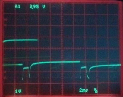
Figure: Lamp Pulses in Water As Through 100 kΩ Broken Seal Resistance, A3030D. Vertical scale 1V/div and 0V is the major division just below the lowest extent of the signal. Horizontal scale 2 ms/div.
The voltage in B during the pulses is always 1.3 V above X−, or 2.5 V with respect to 0V in the circuit, because X− = VCOM = 1.2 V. The L+ and L− leads are at +5V and 0V respectively during a 100% pulse, so their average voltage is 2.5 V. The 100 kΩ resistor carries this 2.5 V to B and we measure it with respect to X− as 1.3 V. When the lamp is off, the average potential of the lamp leads is erratic. We suspect a bug in the firmware: the lamp leads should be in the same state at the end of every pulse. Between some pulses, B reaches 3.8 V, which is 3.8 + 1.2 = 5.0 V above the 0V of our A3030D circuit, consistent with both lamp leads being at +5V, which is what we expect between pulses.
In most pulses, B reaches only 1.8 V, or 4.0 V with respect to circuit 0V. We look at the lamp leads directly and find their voltages are erratic at the end of the pulse, as if Q1 is sometimes switching off before we turn off the boost regulator, and sometimes after. We replace D7.12 with C6.7 and obtain consistent, uniform pulses in B.
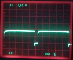
Figure: Lamp Pulses in Water As Through 100 kΩ Broken Seal Resistance, A3030C. Vertical scale 1V/div and 0V is the major division just below the lowest extent of the signal. Horizontal scale 2 ms/div.
We replace 100 kΩ with 10 MΩ. The variation in B is 200 mV dominated by 60 Hz, and with average value 0.7 V. We place the lamp in B and voltage in B is the same as for 100 kΩ bridge. We remove silicone and burn off epoxy to get to the A3030C 0V terminal. We ground our probe to 0V and measure B. Lamp-on voltage is 2.2 V, lamp-off is 4.4 V. We connect 0V to B with a wire. Average voltage of B now 0.7 V with pulses 60 mV as shown below.
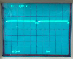
Figure: Lamp Pulses in Water With Grounding As Through 100 kΩ Broken Seal Resistance, A3030C. Vertical scale 200mV/div and 0V is the major division just below the lowest extent of the signal. Horizontal scale 2 ms/div.
The wire from 0V to B reduces the amplitude of the pulses in B from 1.4 V to 60 mV. In X the lamp artifact now fits entirely within the 30-mV dynamic range of the input. With a 10-MΩ bridge resistor, lamp artifact on X drops to 500 μV. With 100-Ω bridge the pulses in B are 500 mV. If we move the ground clip to touch the end of the 100-Ω bridge, the pulses in B drop to zero. We move the 0V connection to A, near the 100 kΩ bridge, and place the LED on the far side of A. The voltage in B varies with the pulses by 1V from a minimum of 1 V.
[04-AUG-17] We have MM-47 compression springs made of 250-μm diameter stainless steel wire. We cut a 10-mm length of spring and to assemble the tunnel-grounding termination shown below.

Figure: Grounding Spring Coiled Around Two Leads.
Here the yellow lead is soldered to the grounding spring. We would rather use green in the future. The red and blue leads are standing in for the lamp leads. We usually use orange and purple. The spring is intended to protrude a few millimeters from the head fixture cement. It is tight on the lamp leads, so that it will make contact with the fluid that lines the lamp lead tunnel out of the head fixture.
[29-AUG-17] We connect a grounding spring to the GND pad next to the lamp leads on A3030E number E157.1. We immerse the LED with its exposed leads and the grounding spring in a petri dish of water. We flash the lamp at 100% brightness. We place the X leads in the water 50 mm away and separated by 10 mm. Lamp artifact is 10 mVpp. Data transmission is interrupted by the switching on and off of the LED when its leads are in water, but not when they are out of water. When the LED is on continuously or off continuously, transmission is reliable. We put the X leads in a separate petri dish of water. Lamp artifact is 85 μV. We connect the two petri dishes with 100 kΩ. Lamp artifact is a 3.2 mVpp triangle wave. With a scope probe we find the second petri dish's potential fluctating by 300 mV with respect to the circuit 0 V. With 10 MΩ between the petri dishes, the artifact is less than 100 μV.
[01-SEP-17] We put the LED in water while flashing and we see no lamp artifact and we get 100% data reception. We place the EEG leads in the same beaker shorted together with a clip. Reception is 100%. With a scope probe we see the water voltage varying from 1.2 V to 3.0 V with occasional diversion to 5 V. In X we see 100-μV pulses most of the time, with occasional diversions of 1 mV. The lamp flashing in this version of the firmware is irregular, and we have previously noted the absence of these 5-V diversions in the A3030C firmware. Assuming we fix this irregularity in the A3030E firmware, the lamp artifact is 100 μV for 1-V pulses. We disconnet the EEG leads. They are separated by 10 mm. Lamp artifact is now a rolling waveform of around 2 mV that conforms more closely to the picture on our oscilloscope.
We slide the ground spring into the water and we now see regular artifact of 1 mV along with interruption of transmission on every lamp pulse.
We remove the ground spring from the water. We now have the EEG leads in a separate petri dish, separated by 10 mm and the LED petri dish connected through a 100-kΩ tunnel simulation resistor. Water voltage in LED petri dish is 1.2-2.5 V. In EEG petri dish it is 1.2-1.6 V. Lamp artifact is 500 μV. We place the ground spring in the second petri dish in contact with the 100-kΩ resistor. Lamp artifact is 20 μV. We move the resistor 20 mm from the ground spring. EED dish voltage is ±10 mV. Lamp artifact is 50 μV.
We use a 0-Ω tunnel resistance ending 20 mm from ground spring. EEG petri dish voltage ±0.2 V. Lamp artifact 1 mV with loss of data transmission. The GND potential of the A3030E, which is also its 1.2-V logic power supply, is varying from 1.2-1.4 V. We connect the LED dish through an ammeter to the ground spring and get an average current of 250 μA. The effective output impedance of our voltage regulator is 400 Ω. Given the avearge voltage in the water is 2.5 V, the effective water resistance is 5 kΩ. The 1.2-V reference voltage for the five-bit DAC is increasing by 20%, which will increase the RF center frequency by around 10 MHz and so disturb reception. Our Spectrometer shows the transmit power spread across 912-926 MHz.
[06-SEP-17] We construct a head fixture out of dental cement for E157.2. We leave the grounding spring protruding from the cement, as shown below. We let the cement cure, then pull on the lamp leads twenty times to make sure the seal around the silicone lamp leads is broken. In water, the impedance between L+ and GND is 1.1 MΩ, and between L− and GND is 0.4 MΩ. We solder the lamp and ground leads to E157.2.
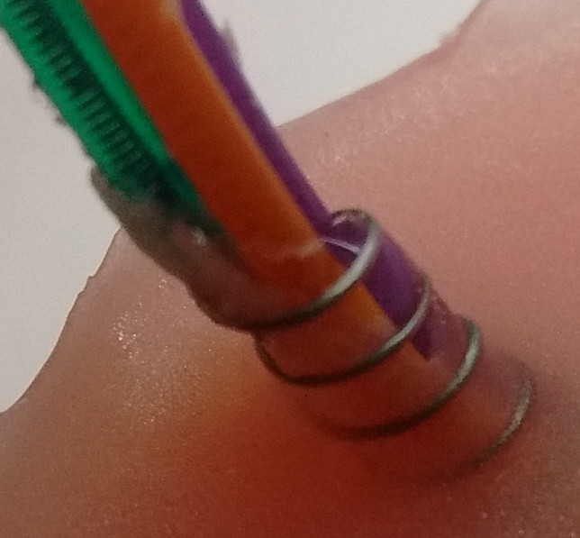
Figure: Grounding Spring Emerging from Cement.
We flash the lamp at 10 Hz with 50-ms pulses of full power. We place both EEG leads in the same water reservoir as the head fixture, on opposite sides. E157.2 does not have capacitors C9 and C15. The water potential is a 20-mVpp high-pass filtered square wave with 10-mVpp high frequency overlayed when the lamp is on. We see a 140-μVpp triangle wave on X. We remove both EEG leads and see total noise 8 μV rms. With just the X+ lead in the water, we see a 5-mVpp triangle wave. We connect both EEG leads together in the water with a small alligator clip and see 8 μV rms total noise.
[08-SEP-17] We generate a 100 mVpp square wave at 10 Hz with a 1.2-V offset. We pass this through a resistor R and into a dish of water. We have E157.2 without C9 and C15 and lamp leads removed. We have only a ground wire with a spring on the end. We place the EEG leads in water with R = 50 Ω. We see a triangle wave on X with amplitude 7 mVpp. We place our ground spring in the water and the wave is a spikey square of 8 mVpp. We set R = 100 kΩ. Without the ground spring we have a triangle wave of 3.7 mVpp. With ground spring in water we get 320 μV triangle. If we touch the ground spring to the wire delivering the square wave to the water, we get total noise 10 μV. With the ground spring 20 mm from the delivery wire and the EEG leads connected either by a solder joint or a clip, we get total noise 8 μV.
We make several head fixtures and try to break their tunnel seals to measure lamp artifact with head fixture in water. In pulling on the lamp leads to break the seal, we end up breaking one or both wires, which we do not discover until much later, after many measurements. We resolve to go back to simulating a seal failure.
We connect a lamp to E157.2 and place the lamp in dish No1. We connect dish No1 to dish No2 with 100 kΩ. We place our ground spring in dish No2. The voltage in dish No1 is a 300 mVpp square wave. In dish No2 we see a 10-mVpp square wave. We place our two EEG leads with square-cut ends in dish No2 and see a 230-μVpp square wave. We remove 3 mm of silicone from the ends and see a 500-μVpp triangle wave. We connect the two leads with a clip and see 15 μV rms total noise. We connect them each to a clip in water but not in contact. We see a 500-μVpp square wave. We remove the clips and connect the ground spring to the bridge from dish No1. We see total noise 20 μV rms. We flash 10-ms pulses at 10 Hz and see spikes 1 mVpp. Instead of our 1V2 ground, we ground dish No2 with a 0V wire. We see a 1.5 mVpp square wave.
We remove the lamp from dish No1. We apply a 100-mV 10-Hz square wave to dish No1 with respect to the ground spring. The voltage in dish No1 100 mVpp. In dish No2 we see <2-mVpp of 10 Hz. We place our two EEG leads with 3-mm stripped ends in dish No2 and see a square wave with spikes 240 μVpp or 60 μV rms. We clip the two EEG electrodes together and see total noise 6 μV. We place clips on both leads but separate and see less than 20 μV of 10 Hz. Remove the clips and we are back to 240 μVpp with 3-mm wires.
We replace R5, R6, R19, and R20 with 1.0 MΩ 1%. We set up the same experiment. We see 100-500 μVpp square wave. We apply the square wave with respect to 0V and see 300 μVpp. Connect EEG leads together and we see 8 μV rms total noise. We connect a lamp to E157.2 and place the lamp in dish No1. We disconnect our function generator. We flash the lamp at 10 Hz 50%. We see a 500 μVpp square wave on X. In dish No2 we see 10 mVpp with respect to 0V.
[11-SEP-17] We have dish No1 and No2 as above. We intend the grounding spring to act as a shield around the tunnel fluid. We connect dish No1, which contains the bare flashing LED, to dish No2 with a resistor. We place the resistor wire in the center of E157.2's grounding spring. (At this point, E157.2 has 1-MΩ resistors in its differential amplifier, and no C9 or C15.) To separate the spring and the wire we wrap the wire in tissue paper.
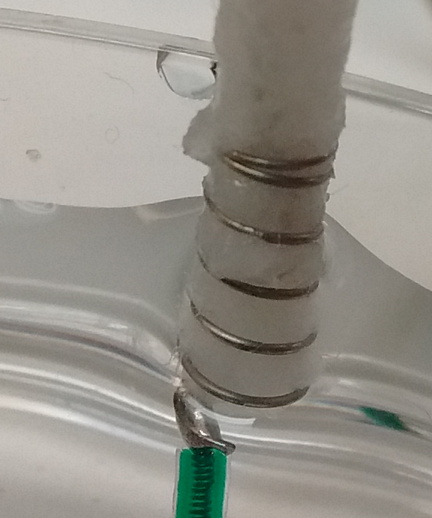
Figure: Spiral Shielding by the Grounding Spring. The lamp current arrives through a wire at the center of the spring, separated from the spring by wet tissue paper.
We set the bridge resistance to 0 Ω, a wire only. We flash the lamp once for 50 ms. We see a 2 mV 1-s pulse on X with the EEG leads separated by any distance, and also if they are connected by a clip. The potential in dish No2 is varying by 200 mV and so is the GND potential. We set the bridge resistor to 100 kΩ. With the leads clipped together the lamp artifact for the 50-ms solitary pulse is less than 50 μV. With EEG leads 50 mm apart, the artifact is 100 μVpp. We flash for 50 ms at 10 Hz and see total noise 20 μV rms on X. With a ×1 probe we see 10-Hz 5 mVpp square wave throughout the dish. The pulses in X are around 50 μVpp regardless of where we place the EEG leads: together, connected, or separate. The GND = 1V2 potential is varying by 5 mVpp, and so is VC. The differential amplifier measures only the difference in potential between points in dish No2, subject to the effect of its input impedance upon the field in the dish. The common-mode input impedance is 2 MΩ in E157.2 now, with its 1-MΩ resistors. If the input resistance were affecting the field asymmetrically, we would see variation in the artifact with lead position, but we do not. The artifact is due to the change in VC at the input of the ADC, 5 mV as a proportion of 3 V being 100 ADC counts, or 46 μV apparent in X.
We vary brightness. Peak to peak 10-Hz artifact on X with 50 ms flashes at 10 Hz is ≤20 μV for 0%, 40 μV for 20%, 80 μV for 40%, 80μV for 60%, 30μV for 80%, and ≤20 μV for 100%. These values for brightness 20-80% are an order of magnitude lower than we expect for E157.2 given that its EEG input is not equipped with capacitors C9 and C15. But in this arrangement, the lamp leads are far from the EEG leads, and the 1-MHz brightness modulation signal is coupled into the EEG leads by proximity. We are ignoring the frequent solitary pulses on X that are a result of a bug in the A3030E firmware.
[12-SEP-17] The anode of the LED attached to E157.2, which we have been leaving in dish No1, has corroded in preference to the cathode. We remove the battery from E157.2 every time we end an experiment, so this corrosion has occurred during our extended periods of 50% flashing.
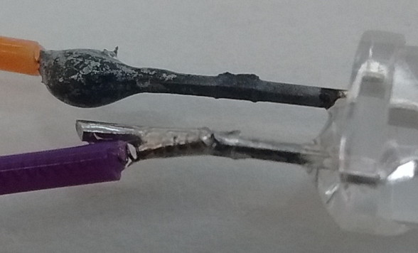
Figure: Corrosion of the LED Anode.
We modify the P3030E firmware. We turn on the boost converter only during lamp pulses, we keep the transmit clock running the entire stimulus, and we modulate and turn off the lamp only with Q1. We set up yesterday's experiment with dish No1 and No2, 100 kΩ bridge and spiral grounding around the bridge. With 50-ms flashes at 10 Hz we see 80-μV lamp artifact during the stustained stimulus, as shown below. We move the leads around, close together, apart, and clipped together. The artifact varies in amplitude from 60-100 μVpp, and from triangle wave to rounded square wave. When we reduce the bridge resistance to 0 Ω we see this 800-μVpp artifact.
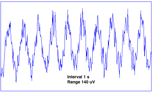
Figure: Lamp Artifact for 50 ms flashes at 10 Hz with Spiral Ground and 100 kΩ Bridge.
We now flash the LED for a single pulse of 50 ms, stimulus length 50 ms and 100% brightness. We observe the following 800 μVpp artifact for bridge resistance 100 kΩ and this 2.2-mV artifact for 0-Ω bridge resistance. When we remove the lamp from dish No1, all the above artifacts reduce to below 20 μV.
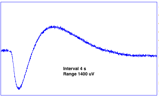
Figure: Single Pulse Artifact 50 ms Solitary Pulse with Spiral Ground and 100 kΩ Bridge.
We modify the P3030E firmware so that Q1 is off and the boost converter is on during the entire stimulus, so we can see boost converter artifact. The lamp is in dish No1, where the voltage is 5 V with 20 mV of 800-Hz converter artifact. Total noise on X is 10 μV. We modify firmware again so the boost converter is on during the entire stimulus and the lamp is modulated only by Q1. Our bridge resistor is 100 kΩ. At 100% brightness dish No1 is at 4.3 V when the lamp is off and 2.5 V when the lamp is on. Lamp artifact is 250 μVpp. The artifact reduces with brightness, dropping to 100 μVpp at 20% and <20 μVpp at 0%. When the stimulus ends, dish No1 drops to 1.2 V to match dish No2. The one-pulse stimulation artifact is 800 μVpp. For 10-ms pulses 100% brightness 10 Hz, our lamp artifact is 150 μVpp.
[13-SEP-17] We have E157.1 with its 1 MΩ for R5, R6, R19, R20 and 0 pF for C9 and C15. We set up a two-dish artifact experiment with 100 kΩ bridge. We see 60 mVpp 10-Hz square wave in dish No2 with 50-ms 10-Hz full power pulses. We see a 500 μVpp triangle wave on X. We have E157.1 with its 100 kΩ for R5, R6, R19, R20 and 100 pF for C9 and C15. We repeat the same experiment, making sure dish No2 is 60 mVpp. We see a 5 mVpp triangle wave on X. We remove C9 and C15. In dish No2 we now see only 20 mVpp. On X we see a 2.5-mV triangle wave.
We have E157.2 with 1 MΩ resistors. We arrange lamp and EEG leads in parallel and clip the EEG lead ends together. We flash at 60% power and see 400 μVpp square wave. With E157.1 100 kΩ we see 1 mVpp.
We connect the 100 kΩ bridge resistor to the grounding spring in dish No2. We flash at 10 Hz 50 ms full power. E157.2 sees <10 μVpp artifact. At 60% power it sees 500 μVpp artifact. But E157.1 sees 50 μVpp at full power and at 60% power 5 mVpp. In both cases the artifact is ten times greater with the 100 kΩ amplifier resistors.
[15-SEP-17] We add 1 tsp of granulated table salt to 500 ml of hot water to make a 1.2% saline solution (the density of granulated table salt is around 1.2 g/ml and 1 tsp = 4.9 ml). We set up the following apparatus to measure impedance.
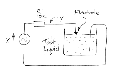
Figure: Apparatus for Measureing Saltwater Impedance. The ground wire is solid copper coated with tin. With a stainless steel electrode, and the voltage source X disconnected, we see a galvanic potential of 220 mV at Y with respect to the ground wire, which is consistent with a galvanic cell made of steel and tin.
We begin by calibrating our apparatus with a 10-kΩ resistor in place of R2. We apply X = 0 mV and observe Y = 0 mV. We apply 1 Vpp sinusoid from 10 Hz to 5 MHz and see Y = 500 mVpp with negligible phase shift up to 100 kHz. At 1 MHz we have 420 mVpp and 120 ns delay.
We insert a stainless steel 00-80 screw electrode through the surface of the saltwater, so that it forms a hemispherical electrode of diameter 1.6 mm. We set X = 0 mV and observe Y 8 mV. We disconnect X and see Y rise to 220 mV over the course of a minute. Ambient temperature 24°C, saltwater at 30°C. Two hours later, with the water at 26°C we see 200 mV. Our stainless steel screw, saltwater, and tinned ground ground wire are acting like a 220 mV battery with a 300 kΩ source impedance. We note that the galvanic potential of stainless steel is around −0.1 V and that of tin is around −0.3 V, for an expected galvanic cell voltage of 200 mv. We apply sinusoids of increasing frequency to X and measure the amplitude and phase of Y.
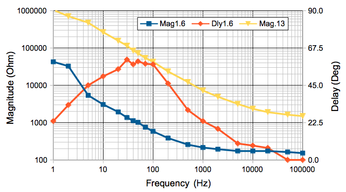
Figure: Impedance of Saltwater Electrodes. Mag1.6: Magnitude of 1.6-mm diameter screw impedance. Mag.13: Magnitude of 130-μm diameter wire tip impedance. Dly1.6 phase delay from X to Y for 1.6-mm electrode and R1 = 10 kΩ.
We cut a teflon-insulated stainless steel wire of diameter 130 μm and use its tip as an electrode in place of our screw. The saltwater system now genrates 100 mV with a 5 MΩ source impedance. We measure amplitude and phase of Y with frequency, but we have to vary R1 from 10-200 kΩ to obtain reliable measurements. At 50 Hz and R1 = 100 kΩ we see the following on X and Y. The asymmetry of Y implies that the resistivity of the saltwater system is non-linear.
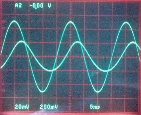
Figure: Asymmetry of Saltwater Electrode Impedance. The non-linear impedance of the electrode will allow it to demodulate radio signals, so it is, in theory, possible for an EEG electrode to pick up a powerful amplitude-modulated radio station.
The frequency dependence of the electrode impedance is not consistent with a capacitance in parallel with the electrode resistance. We could construct a model that approximated the frequency response with two capacitors and two resistors, but the asymmetry Y is inconsistent with any model made of such linear coponents.
According to our calculations, the impedance of a hemispherical electrode of radius a should be ρ/2πa, where ρ is the fluid resistivity. Our 1.6-mm diameter measurements imply ρ = 15 Ωm at 10 Hz and 3.0 Ωm at 100 Hz. Our 130-μm wire tip has the same area as a hemisphere of radius 46 μm, so we expect its impedance to be 17 times greater than the 1.6-mm screw tip. At 10 Hz it is 100× greater, and at 100 Hz it is 74× greater. We examine the end of the wire under a microscope and so far as we can tell, the flat end of the wire is exposed, with the insulation frayed but well clear of the tip.
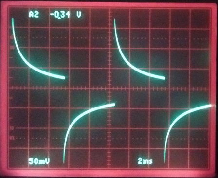
Figure: Current Spikes Between Electrodes and Saltwater. We apply a 100-Hz, 1-Vpp square wave to a 1.6-mm diameter hemisphere electrode and a large ground electrode. The time scale is 2 ms/div and the current scale is 500 μA/div.
The figure above shows 2-mA current spikes through our 1.6-mm diameter electrode when we apply a 1-Vpp square wave. Our lamp artifact will be a similar square wave, and it's clear that we will see the spikes of the artifact coming through the tunnel fluid, with the same amplitude for pulses of 1 ms to 1000 ms. Our chief concern is the resistivity of the body fluid at 100 Hz, where our EEG amplifier has full gain and resistivity is low. So we will use 3 kΩmm for the worste-case resistivity of the tunnel fluid.
We apply dental cement to a ground spring wrapped around two lamp leads. We have two 3-mm heat shring collars between the spring and the LED, which we shrink while stretching the leads so that they are a tight fit. After 5 minutes the dental cement is still tacky. After 15 minutes it is hard. We pull on the lamp leads and we can drag them through the spring until the collars press on the cement. But we cannot pull hard enough on the wires to move the collars. The lead insulation tears before we can put enough force on the collars.
[21-SEP-17] We test the performance of the A3030E grounding spring and differential amplifier, and report here.
[13-OCT-17] We construct a head fixture out of epoxy without grounding, see here. After two hundred tugs followed by one day soaking in saltwater, we see the following artifact when we flash at 100% power for 10 ms at 10 Hz with the EEG leads in the water but the grounding lead in air.
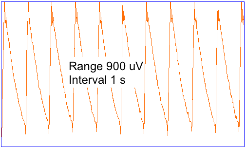
Figure: Artifact for Broken Seal In Epoxy, Without Water Grounding. The two EEG leadsa are immersed in the saltwater with the epoxy head fixture, but the grounding lead is in air.
When we immerse the ground wire in the same body of saltwater, we get the following artifact.
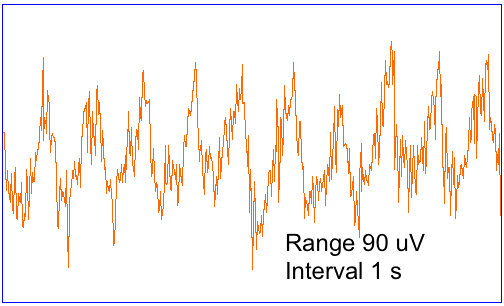
Figure: Artifact for Broken Seal In Epoxy, With Water Grounding. The two EEG leadsa are immersed in the saltwater with the epoxy head fixture and the grounding lead is in air.
The grounding lead reduces the artifact by a factor of twenty. The artifact without grounding is less than 1 mVpp through the epoxy tunnels.
[20-OCT-17] During our lamp pin corrosion experiments, we at one point notice that flashing the lamp in our flask of saltwater causes artifact in a transmitter in air outside the flask.

Figure: Lamp Artifact for A3030E in Saltwater (Orange) and in A3028D in air (Blue).
The lamp flashes are 10 ms at 10 Hz, full power. We see 400 μVpp spikes induced in the 10-MΩ input of the A3028D during the flashes. The artifact in the A3030E itself, meanwhile, is only 50 μVpp.
Lamp Pin Corrosion
[10-OCT-17] We leave an A3030E inactive in tap water for three days with the two lamp pins separated by 5 mm. We see a white residue on the L− pin. After a week, the L− pin has green residue all over it and it breaks in half when we try to scrub it clean in water.

Figure: Corrosion of Negative Lamp Joint after Three Days In Water. The lamp was off for the entire three days, and the device was inactive.
The charging diodes D4 and D3 CMDSH2-3 are reverse-biased, but they are Schottky diodes chosen for their low forward voltage during charging, and their reverse leakage current is of order 2 μA. This current flows out of the L− lead. Hydroxide ions in the water give up an electron to carry the current, resulting in a metal oxide and half a hydrogen gas molecule. The stainless steel springs do not corrode, even though we expect iron to corrode preferentially to copper during voltage=driven corrosion.
Figure: Recharging Diodes. Diodes D3 and D4 conduct during charging. Their reverse leakage current flows between the lamp pins through water when the device is inactive.
We encapsulate two lamp leads with an LED in clear epoxy. The lamp is attached to E157.3. A better choice of diode would be one with far lower leakage current, such as a PN-junction small-signal diode. We connect the cathode of a 1N4448 to +3V, a wire to the anode, and a wire to 0V. We put the far ends of the wires in water. The anode wire models the L− wire in the A3030E, but the 1N4448 reverse leakage current is of order 20 nA. We will see how fast the anode wire tip corrodes.
[11-OCT-17] We have our LED in clear epoxy. We cover with 1.2% saltwater and pull with 1 N force on the leads 200 times. The seal on the leads remains unbroken.

Figure: Lamp Encapsulated in Clear Epoxy, Before Immersion. Note the clear epoxy dome of the LED is almost invisible now that it is immersed in a larger body of clear epoxy.
We pull harder on the lamp 10 times, but we still cannot break the seal. Lamp artifact with EEG leads and lamp immersed in the same saltwater reservoir remains less than 10 μV. In our 1N4448 corrosion test, there is no sign of discoleration upon either lead immersed in water.
[12-OCT-17] Water has crept along the outside of the silicone insulation of our lamp leads where they pass through clear epoxy to the LED solder joints. With the EEG leads in saltwater along with the epoxy-filled petri dish, we see 50-μVpp pulses when the lamp flashes. When we immerse the grounding lead in the water as well, lamp artifact drops to below 10 μV rms.
[13-OCT-17] When we pull on the lamp leads, we can see water moving in the gab that opens between the silicone insulation and the epoxy tunnel. Lamp artifact without grounding is 800 μVpp. With ground it is 40 μVpp. We see no corrosion residue. The exposed metal appears has a gold-colored tint to it, even inside the LED package. The clear epoxy we use also has the same gold-colored tint when we look through it.
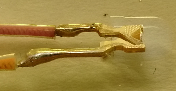
Figure: Lamp Encapsulated in Clear Epoxy, Day Three of Immersion.
In our 1N4448 corrosion test, there is no sign of discoleration upon either lead immersed in water. This contrasts with the CMDSH2-3 diode, where corrosion solids are visible after only one day. The resistance through the tap-water in the beaker is 2 MΩ as measured by the probes of a DVM. The 1N4448's 20-nA leakage current developes a voltage of 40 mV through the water.
[16-OCT-17] We see signs of corrosion on the L− lead in our epoxy-sealed LED.
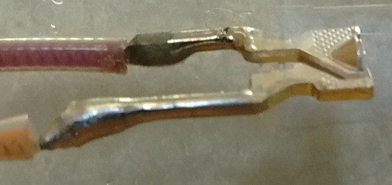
Figure: Lamp Encapsulated in Clear Epoxy, Day Three of Immersion.
We lower the ground lead into the water and leave it there from now on, but taking care to keep the lead-extension joints in the lamp leads out of the water. We flash the lamp for 10 ms at 10 Hz on full power and see 14 μV rms lamp artifact. Battery voltage is 3.7 V. In our 1N4448 corrosion test, there is still no sign of discoleration upon either lead immersed in water.
[17-OCT-17] Corrosion much the same as yesterday in epoxy head fixture. Lamp artifact 27 μV rms. No visible corrosion in 1N4448 test.
[18-OCT-17] Corrosion much the same in epoxy head fixture. Lamp artifact 60 μV rms. No visible corrosion in 1N4448 test.
[20-OCT-17] Corrosion on solder leads is now dark gray, as shown below. Lamp artifact is 16 μV rms.

Figure: Lamp Encapsulated in Clear Epoxy, Day Ten of Immersion.
[23-OCT-17] Corrosion on Day 13 for epoxy fixture is much the same as Day 10. The lamp won't flash more than a few times, but transmission works fine and battery voltage reports 3.7 V. This E157.3 device is the one with the damaged battery case that we sealed with epoxy. We attempt to re-charge, but something overheats next to the lamp leads. It is possible the lamp stimulus is still running, even though the lamp is not flashing, and we are running current through the lamp switch, overheating both the transistor and the charging diodes.
[24-OCT-17] E157.3 still transmitting. Cut away encapsulation around battery tabs and measure VBAT = 3.65 V. We apply recharge directly to battery and see 20 mA flowing in from 4.3 V in a few minutes. We burn away epoxy around lamp leads. We see no sign of corrosion. We remove lamp leads. We start a stimulus. We have L+ = 5.0 V with 100 mV triangle wave from boost converter. We see switching signal on ONL. When we connect a lamp, VBAT drops to about 1.2 V with spikes at the same frequency as the triangle wave. The output resistance of the battery is too great to power the lamp. We claim this high output resistance is a consequence of the breech of the battery case by our sanding wheel during encapsulation.
We pull the purple and orange wires out of our epoxy fixture. The purple wire snaps where it emerges from the silicone, which is where we scratched it before removing insulation. The orange wire breaks at the edge of the solder joint. We remove silicone from the end of the purple lead and examine the steel. The surface is untarnished.
No visible corrosion in our 1N4448 test, which we now terminate after 14 days. We conclude that the 10-nA leakage current of the 1N4448 causes negligible corrosion, and we should load a similar diode in future re-charging circuits. We conclude also that the corrosion caused by the 2-μA leakage current of the CMDSH2-3 does not spread to the stainless steel of the leads, nor parts on the main device, and is suppressed cement on the surface of the copper parts.
Batch ISL4C
[05-SEP-14] We assemble seven A3030As. Together with our existing A3030X prototype, they make a total of eight circuits. We load antennas and tune all eight crystal radios to 146±0.5 MHz. We have 8.0 pF for C8, and we add between 0.0 pF and 1.5 pF to bring the tank resonance to 146 MHz. We number these eight circuits No1.1 to 1.8. They are A3030A assemblies: no EEG circuits loaded, command reception implemented, lamp drive loaded.
[08-SEP-14] We use firmware P3030X10.vhd to program our eight A3030As. We compile a different jedec file for each device id, going from 1.1 to 1.8. We measure inactive current, active current with lamp turned off, and active current with lamp turned on. We correct a few problems on the boards during our tests.
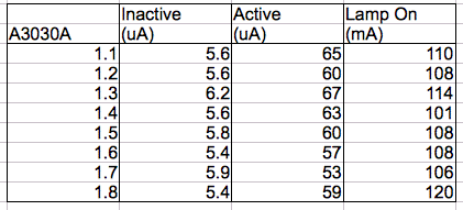
Figure: A3030A Input Current when Inactive, Active, and Active with 70 mA Lamp Current. The battery voltage drops to around 3.3 V when the lamp is on, as a result of the resistance of our ammeter. To measure the inactive current, we connect power and wait for two minutes.
The inactive quiescent current is around 4 μA for the first few seconds we connect power, increases to almost 7 μA for a minute, then drops to the values we list above.
[15-SEP-14] We have encapsulated No1.2-1.8 in the following manner. We remove all insulating and binding tape from a GM382030 LiPo battery. We solder its tabs to our A3030A circuit board. We apply three coats of acrylic conformal coating to both sides of the circuit board. We cover the top side with optically clear E-30CL epoxy and press the battery down upon the glue. We lay the circuit on teflon with the battery down. We apply the same glue to the bottom side, which is not facing up. We allow to cure. In most cases, some glue has dripped down off the circuit board, around the battery, and onto the teflon. We clip and filed the excess glue from around the battery. We applied two layers of acrylic coating to the battery leads. We hung the devices by their antennas, so they were vertical, and dipped four times in silicone. Today we filled a few bubbles and covered the top-side sharp corners of the circuit boards.
[17-SEP-14] We have seven encapsulated A3030As. We are happy with six of them. No1.7 has a hole in the battery flange from over-enthusiastic trimming of the excess epoxy. We test No1.3, 1.4, 1.5, 1.6, and 1.8 to ION. We ship these along with five head fixtures, two antennas, one Command Transmitter, and two ethernet cables.

Figure: ISL Stage 4C Deliverables. We have (1) Rubber Duck antenna, (2) telescoping half-wave antenna, (3) Command Transmitter, (4) Head Fixtures A3024HDC-B, (5) Implantable Lamps Circuits A3030A.
Not included in the shipment is the boost power supply for the Command Transmitter. We believe ION still has the boost power supply from ISL Stage 4B, while will do the job.
[08-OCT-14] A3030A No1.2 has been in water for a 9 days. It still works fine. Now place it in saltwater.
[22-OCT-14] A3030A No1.2 has been in water for a 23 days, most of that in salt water. It still works fine.
Batch ISL5
[24-OCT-14] We have 30 of A3030B assemblies, fully-populated on the improved A303001B circuit board, which includes rounded edges and all modifictions necessary to the A3030A. We attach antennas and program with the P3030B04.vhd firmware. Even before calibration of the ring oscillator, data transmitter, and crystal radio, we obtain reception of commands and data. We can stimulate the lamp output and record mains hum.
[07-NOV-14] We have antennas, lamp leads, and electrode leads loaded on six A3030Bs, No2.1-2.6. We tune their crystal radios using the apparatus we describe above. We program all boards with firmware B04.
[11-NOV-14] We have six head fixture tapers glued to LEDs and two guide cannulas glued. We have all leads and antennas loaded. We measure quiescent current of the circuits, and calibrate their ring oscillators and radio frequency oscillators. We speed up the ring oscillator to give us more resolution, by removing one gate, so we now have firmware P3030B05.vhd.
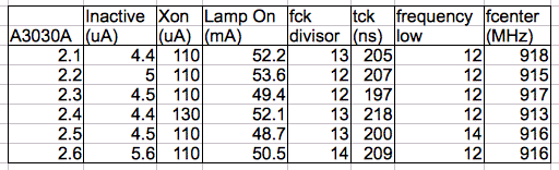
Figure: ISL Stage 5 Quiescent Current and Calibration Constants.
The quiescent current of 2.6 is correct except for one anomaly. When we turn off data transmission, current drops to 5 μA, rises to 90 μA, and drops to 5 μA again, where it remains. The rise and drop take about twenty seconds. We programmed another circuit and it had the same behavior, but No2.1-2.5 do not exhibit the rise and drop.
The Lamp On current is with an EZ500 connected to the organe (L+) and purple (L−) leads. We measure the total resistance of these leads, and it is 60-70 Ω, average of 65 Ω across the six A3030Bs. We measure the lamp current at 35 mA, a little short of our target 40 mA.
[14-NOV-14] We loaded batteries on No2.1-2.6 using solder with aqueous flux. We washed the battery tab joints, being careful not to soak the battery. But No2.1 and No2.6 do not respond afterwards. We unsolder battery and resolder, and they respond for a while. We think we have them fixed and dried, then we apply epoxy and discover that they don't work.
The photograph below shows our ISL Stage 5 Delivery. We have five A3030B ISLs and 5 A3024HFC-B Head Fixtures. The No2.1 ISL failed during encapsulation, so we are sending it as a physical sample.

Figure: ISL Stage 5 Deliverables. We have 5 Head Fixtures A3024HDC-B and 5 ISL A3030B. The ISL No2.1 is non-functioning. The purple and orange leads are L+ and L−, the lamp connections. The red and blue leads are X+ and X−, the EEG connections. We see the two-turn command antenna bound up with the one-turn data antenna.
The head fixtures are No3.4, 3.5, 5.1, 5.2, and 5.2, which produce 13, 13, 13, 15, and 14 mW blue light respectively at their fiber tips when supplied with 40 mA forward current. The A3030B lamp current leads have resistance roughly 65 Ω, compared to 55Ω for the A3030A leads. As a result, the lamp current is closer to 35 mA, so the light emitted by the fiber tips for these devices will be around 12 mW. Accompanying these circuits, we have the ISL Controller Tool, Version 2.2, which fixes some device-addressing problems present in Version 2.1.
[15-JAN-15] In November, before we shipped the ISL5s, we put one in water with a head fixture and observed up to 10 mV of switching noise on the EEG monitor when we flashed the lamp. The amplitude of the noise did not correlate well with proximity of the lamp and the EEG leads. After half an hour of work, we ran out of time to examine the problem. Since then, Rob Wykes has implanted No2.5 and observes the following noise on the EEG signal during 18-Hz, 10-ms optical pulses of 0-100% power.

Figure: Lamp Flashing Noise on EEG Input. ISL No2.5 is implanted in a rat.
Detail of the 20% power noise, shown below, shows a rising and falling edge on the pulse start and stop, and another 130-Hz interference that we see also when the light power is 0%.

Figure: Lamp Flashing Noise on EEG Input for 20% Power, Detail. ISL No2.5 is implanted in a rat.
We believe both these types of noise are electrical and magnetic, rather than photovoltaic. The boost regulator runs even at 0% power, so its switching noise is most likely the source of the persistent 130-Hz. The large spikes when the lamp switches on and off may be due to proximity of the four leads, or be electrical through the body fluids. We do not see such noise when the devices are unencapsulated and in air.
[27-FEB-15] We compare reception of repeated commands by the A3024A and the A3030A. We fasten an example of each to a piece of cardboard.

Figure: Two ISLs Strapped to Cardboard for Command Reception Test.
We use our 146 MHz Command Transmitter (A3029A) to produce commands for the A3030A, with the correct checksum and byte instructions. When the RF power turns on, the A3024A picks it up and turns on its light also. We measure maximum range of reception, for a favorable orientation, and maximum range for reception in 95% of orientations. We also test reception with the two devices in water.

Figure: Two ISLs In Water for Command Reception Test.
We measure maximum range for reception in water. We add 5 g of salt to the 500 ml of water and stir until dissolved. We measure maximum range again.
| Test | A3030A No1.2 | A3024A No7 |
|---|
| Robust Reception Range on Cardboard | 70 cm | 100 cm |
| Maximum Range on Cardboard | 250 cm | 600 cm |
| Maximum Range Held By Lamp and Dangling | 300 cm | 900 cm |
| Maximum Range in Water | 70 cm | 450 cm |
| Maximum Range in Saltwater | 70 cm | 450 cm |
Table: Comparison of Reception for Encapsulated A3024A and Encapsulated A3030A.
It occurs to us that encapsulation or an exhausted battery might affect No1.2's reception, so we try an un-encapsulated A3030B with a fully-charged battery and measure maximum range in air. We get 250 cm, the same as for No1.2. We walk around with the lamp held in our fingers, and the device dangling below, and repeat our measurement of maximum range.
Batch ISL6
[05-MAY-15] We program and calibrate A3030C circuits C6.1-7. Calibration and test results below. We measure active current by shorting OND to VB. Our VB is 4.28 V, so R22 draws 130 μA, which we subtract from total current consumption to get the consumption of our A3030C circuit when active with its ring oscillator running and state machines at the ready, but neither transmitting nor flashing the lamp. The A3030C can be active for almost 3000 hours.
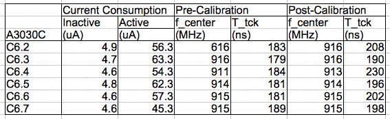
Figure: Calibration Results for C6.2-7. We forgot to measure these parameters for C6.1 before we clipped off its programming extension.
We solder seven 190-mAhr LiPoly batteries to the seven circuits with no-clean, water-insoluble flux. We charge them all until they are full. We remove the positive leads, clip the programming extension off, re-solder the positive lead, and start encapsulation in black epoxy.
[06-MAY-15] We have seven partially-encapsulated A3030C, C6.1-7. We put them in a faraday enclosure in petri dishes and turn them all on. We get the following noise spectrum from all seven.
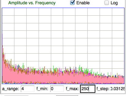
Figure: ISL6 Input Noise.
Total input noise is 8 μV rms. The average value of the signals should correspond to 1.2V, and the full range to 3.0 V, so we use the average value to calculate the 3V0 voltage and get 2.94±0.02 V. Data reception with two A3027D antennas is >95%. Command reception within 30 cm of the command transmit antenna is >95%.

Figure: Batch ISL6 Deliverables. The five encapsulated A3030Cs are on the center right. For a close-up see here. On the left we have antenna cable, LWDAQ cable, and boost power supply for the Command Transmitter 915-MHz (A3029B). There are three BNC feedthroughs to enhance an existing faraday enclosure. Five A3024HFC-B are arranged below. We connect a Loop Antenna (A3015C) to the Command Transmitter with a short coaxial cable and a BNC elbow.
[07-MAY-15] Batch ISL6 is ready to ship. Devices C6.1-7 are all encapsulated in black epoxy, black varnish, and four coats of silicone. All have gain versus frequency within 3 dB of nominal. All respond to commands, respond with acknowledgment, and deliver stimulus to their lamp pins. All have perfect reception in a faraday enclosure, except C6.4, which is the one with TCK period 230 ns. We ship C6.2-3, C6.5-7 to make five for ISL6. We ship A3024HFC-B numbers B2.7, B6.1-3, and B6.8. The Command Transmitter is serial number Q0150 with firmware B1.
[11-MAY-15] We put a self-propelled ball in a latex glove and attach C6.1 to the outside. We place the combination in a tub of water and let the ball move the ISL around through the water. We place the tub in an FE2A faraday enclosure with three data receive antennas and one 915-MHz command transmit antenna. We put the lid on.

Figure: ISL C6.1 Moving in Water.
We measure data reception from C6.1 over one minute and get 92%. We disconnect the A3029B command transmitter from its antenna and get 94%. We turn off power to the 915 MHz oscillator on our A3029B and get 91%. It appears that the command transmitter, when inactive, is not affecting reception.
We use the ISL Controller V3 to request 116 acknowledgments. We receive 100. If we assume loss of acknowledgments occurs at 92% in data reception, we estimate that command reception is 100 / 116 / 0.92 = 94%.
[04-SEP-15] C6.1 responds well to commands, battery voltage around 3.7 V, and reception of data is good. C6.4 does not respond.
We have C6.1, C6.3, C6.6, and C6.7 responding to commands and transmitting EEG. Acknowledgement transmission fails roughly 10% of the time. We have C6.2 and C6.4 with gas pressure inside. Neither of them works. We dissect both of them with intent to upgrade to A3030C-LO.
[17-JAN-17] C6.2 and C6.4 have been refurbished to A3030C-LO and soaked in water for a week. They are still flashing their test lights on command. We remove test lights, dry, and bag ready to ship to ION.
[14-FEB-17] We refurbish C6.3 and C6.6 to A3030C-LO. C6.3 inactive current 6.8 μA, transmit 117 μA, white LED at full power 60 mA. C6.6 inactive 5.8 μA, transmit 117 μA, white LED full power 57 mA.
Batch ISL7
[10-JUL-15] This batch scheduled to ship in the first two weeks of July. We tune all crystal radios, modify all boards for 100 kΩ input impedance and the new lamp switching mosfet. We program D7.1-12. We measure current consumption in various states.
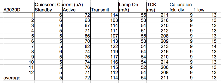
Figure: A3030D Current Consumption. Active is with the logic chip powered up, waiting to flash the lamp. We connect an EZ500C470 to the lamp leads for the lamp on measurement.
We check frequency response with a 4 Vpp sinusoidal sweep 1-500 Hz through 20 MΩ, which produces 20 mV at X. All are within 2 dB of nominal. We heat every circuit until reception stops due to frequency drift in the RF oscillator, then allow to cool, then freeze to −10°C. Reception is robust roughly 0-50 °C.
[11-JUL-15] We re-program D7.1-10 with P3030D06.vhd because they have a potential problem with the ADC conversion. We clip programming extensions and load batteries on to all devices (D7.1-12).
[15-JUL-15] We have D7.1-12 all working. We put them all in water and turn them all on. We measure simultaneous reception with one antenna, the value of the 3-V power supply as deduced from the average value of the signal, and noise in microvolts.
ID RECEPTION (%) VA (V) NOISE (uV rms)
1 93.75 2.92 10.07
2 88.28 2.95 10.49
3 100.00 2.96 14.21
4 95.31 2.94 11.82
5 98.44 2.96 11.78
6 97.27 2.94 11.13
7 98.44 2.98 13.29
8 87.89 2.97 10.76
9 95.70 2.91 8.46
10 95.70 2.96 11.18
11 87.50 2.93 12.60
12 98.44 2.94 11.87
When we turn them all on simultaneously with one command, we get the following traces for their X inputs.

Figure: Twelve A3030Ds Turning On Simultaneously.
The D7.7 device responds differently. We test its frequency response and find it normal. All other aspects of its behavior are normal.
[16-JUL-15] We are shipping the following items today, to fulfill ISL Stage 7. There are ten A3030Ds and fifteen A3024HF head fixtures.

Figure: Batch ISL7 Deliverables. The ten encapsulated A3030Ds are at the center. For a close-up see here. Around the outside we have fifteen A3024HF head fixtures. For details on the head fixtures see the A3024HF manual.
Of twelve A3030Ds we made, 100% of them were fully functional after encapsulation. We ship ten of them, holding back D7.7 and D7.10 because of minor deviations in their behavior from the average. We forgot to bind the X+ and X− leads together before we soldered them to the circuit boards. We likewise forgot to bind the L+ and L−. We bound the leads after encapsulation, which produced an unattractive finish on the previously smooth and rounded silicone-coated springs.

Figure: Imperfect Silicone Binding in X and L Lead Pairs.
We believe there will be no problem implanting these lead pairs, not any compromise of their fatigue resistance due to the cosmetic problems with the finish.
[04-SEP-15] D7.7 responds well to commands, battery voltage around 3.7 V, but reception of data is intermittent on our bench, while reception from C6.1 is good. D7.10 does not respond at all.
[08-SEP-15] We remove silicone from D7.10 battery terminals. Battery voltage is 0.7 V. We solder leads to the battery pads on the circuit board and start to recharge. While re-charging, we turn on and off data transmission, and initiate stimuli. Data reception is perfect. After ten minutes, we disconnect re-charge and the device is running on its own battery. We re-connect re-charge and leave over-night.
[16-FEB-16] We implant D7.8 at ION. An earlier implant is 2 months old in another animal, and head fixture is still intact, but battery has run down. The new implant has leads sealed with collars. Artifact is minimal. Reception of commands is reliable. The head fixture contains a green LED.
[06-APR-16] We have D7.6 back from ION. We expose battery terminals, but when we apply 4.3 V no current flows. We clear more glue and enamel away. We cut the battery tabs to separate them from the circuit board. The positive tab crumbles as we cut it. We pull a sliver of metal that appears to be part of the positive tab out from the battery sleeve and try to charge through that, but still no contact with the battery inside.
[09-APR-16] We work more on the D7.6 battery, exposing the positive battery terminal where it enteres the battery package. But there is no voltage on the terminals, and they will not accept recharge current. We pry the battery off the circuit. It comes off with a little force. We apply external power. Inactive current 5.0 μA. Transmit current 110 &u;A. We measure frequency response as on 10-JUL-15 with external battery. We do the same for D7.1, D7.3, D7.9, D7.11, and D7.12 with their own batteries.
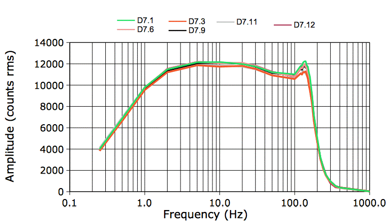
Figure: Frequency Response of Batch D7 on 08-APR-16.
[17-JUN-16] We have three A3030Ds on the shelf. All respond to commands and generate lamp stimulus power. Noise in 30°C water is <10 μV. We measure frequency response.
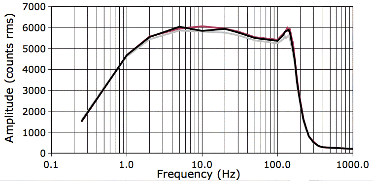
Figure: Frequency Response of Batch D7 on 17-JUN-16.
We take D7.9 and D7.11 and clip all four leads just past the receive antenna. We make two new lamp leads with tapered ends and run them through a dual-bore ceramic collar. We glue the leads in place. We solder a blue LED to the ends of the leads. We solder the leads to the cut-off ends of the original lamp leads. We insulate the cut-off EEG leads and the new joints in the lamp leads. The result is shown here.
[18-OCT-16] We have D7.9 and D7.11 back from ION. Each has been implanted for at least four weeks. D7.11 has a gas bubble in the battery that we can push on, and it smells sweet. It does not turn on. D7.9 has no gas bubble and works. We dissect. The battery voltage is 1.2 V. Disconnect battery and stick a pin into the metal foil to release sweet gas from within. Voltages is 1.0 V. Apply 2.6 V external supply. Current consumption 30 μA. Raise to 3.6 V, 5.4 μA. Turn on with command, 119 μA. We have D7.10 that was working 11-SEP-16 but now has gas pressure inside. Battery voltage 0.0 V. Dissect. Connect external power, get 60 μA inactive and 160 μA active. Wash, bake, inactive current 60 μA. D7.7 works as is, with its battery intact. D7.6 is separated from its battery, inactive 5.8 μA, active 120 μA. Works fine. Replace antennas and lamp leads. Replace C7 with 0.5 pF after knocking off. Remove EEG leads. Active current 114 μA. With 10-ms 100% pulses at 10 Hz, no lamp attached, 170 μA. D7.12 is fully-equipped with leads and encapsulated. It works perfectly.
[24-OCT-16] We have two A3030D-LO devices D7.11 and D7.6 ready to ship to ION. They have no EEG leads, but their EEG amplifier and sample transmitter is operational.

Figure: Implantable Sensor with Lamp, Lamp-Only Version (A3030D-LO).
We take care to make sure the pins are soldered in the correct direction on the leads. Looking at this picture we see that the positive (orange) lead must be in the foreground when the pins are pointing to the left. Otherwise the implanter has to rotate the pins. The length of lead from the collar to the pin is 5 mm so the implanter will not need to fold the leads within the head fixture, but instead can build the head fixture directly over the pins and collar. The devices are encapsulated in black epoxy using our rotator procedure, and then coated in SS-5001 silicone, with extra silicone applied to the sharp corners. The result is not pretty, but it is resilient and flexible.

Figure: A3030D-LO Lamp Artifact.
[16-DEC-16] We have D7.1 back from ION after several weeks of implantation. It turns on and off. No sign of gas bubble or corrosion of the encapsulation. We also have D7.7, D7.9, and D7.12 working perfectly. We dissect D7.1 and D7.7 so as to upgrade to A3030D-LO.
[21-DEC-16] We damaged D7.1 when dissecting. We have D7.7 as A3030D-LO ready for encapsulation. It's inactive current consumption is 5.5 μA, active is 114 μA. We dissect D7.9. Inactive 4.5 μA, active 106 μA. We prepare for encapsulation with a new battery as A3030D-LO.
Batch E157
[21-JUL-17] We have the A3030E circuit board layout A303001C, schematic S3030E_1, and bill of materials A3030E.ods prepared and have asked for assembly quotes.
[25-AUG-17] We have our first two A3030E assembled prototypes. We copy P3030D06 to P3030E01 and program E157.1 and E157.2. We apply external 3.6 V through an ammeter. Standby current 8.2 and 7.8 μ respectively. We have not yet tuned the crystal radio. Nevertheless, we place our 30 dBm command transmit antenna within 1 cm of the single ISL antenna and we are able to turn on data transmission. Active current consumption is 104 and 102 μA respectively. We have 150-mm EEG leads shorted at the tips. We observe electronic noise 7 μV and 7 μV rms respectively. We have white LEDs on the end of 150-mm stretched leads. When we flash the lamps at 10 Hz, 10-ms pulses, noise is 8 μV and 8 μV rms respectively. The spectrum of the electronic noise shows a clear series of harmonics, each with amplitude one or two microvolts. When we turn on the lamp modulation, by specifying brightness 20-80%, we observe lamp noise that varies from 100 μV to 10 mV depending upon how we arrange the EEG leads with respect to the lamp leads. We observe 1 MHz noise being coupled into the differential amplifier U13 and being demodulated into pulses.
We couple RF power into our antenna from our frequency synthesizer. With 0 dBm on the coupling coil, we obtain a peak of 25 mV on VR of at 1.35 GHz and another peak at around 2 GHz. We replace C8 = 0.5 pF with 2.0 pF. Our peak voltage increases, we drop power to −10 dB and obtain a peak of 50 mV at 1250 MHz. We set C8 = 3.9 pF, peak is 20 mV at 1050 MHz. We replace C7 = 0.5 pF with 1.0 pF. Peak 30 mV at 1000 MHz. We try C7 = 0.5 pF and C8 = 4.7 pF and obtain a peak of 30 mV for 0 dBm of 915 MHz and command reception is reliable up to 30 cm. We restore C7 = 0.5 pF and C8 = 2.0 pF and observe peak of 25 mV for −10 dBm at 1200 MHz.
[13-SEP-17] Current consumption of E157.2 with P3030E02 firmware is 7.7 μA in standby, 102 μA with data transmission, and 38 mA when the white LED is on full power. We program E157.1 and get 7.6 μA standby, 103 μA data transmit, and 40 mA at full power.
[15-SEP-17] We have 18 more A3030Es from our assembly company, on 0.031" thick circuit boards. We program 12 of them with P3030E03.
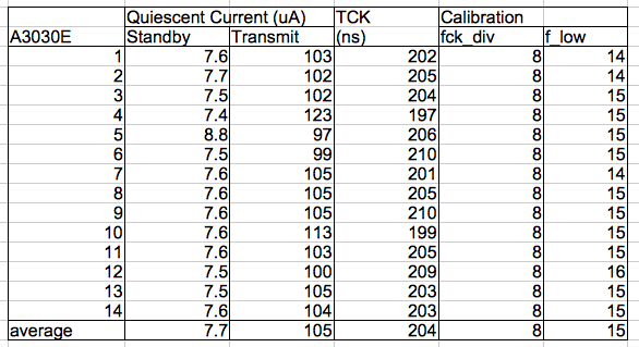
Figure: A3030E Batch E157.1-14 Current Consumption.
The standy current average is 7.7 μA compared to ISL7's 5 μA. The extra 2.7 μA is the current drawn by R3, which we dropped from 10 MΩ to 1 MΩ, so its current increase from 0.3 μA to 3.0 μA. The average transmit current is 105 μA compared to ISL7's 114 μA. This decrease we can explain only as a drop in the quiescent current required by the logic chips.
[19-SEP-17] Device E157.5 is ready for encapsulation, equiped with 130-mm stretched lamp leads. The resistance of the purple lead is 45 Ω and of the orange is 44 Ω. We connect a 3-mm white LED to the lamp pins and turn on to full power. We measure VB = 3.9 V and battery current 35.8 mA. The L− pin is at 1.15 V, making the lamp current 24 mA. The boost converter delivers 127 mA-V and takes in 140 mA-V for effiency 92%.
[21-SEP-17] We have batch E157.3-14 being encapsulated. They all have 100-kΩ resistors in the differential amplifier, and capacitors C9 and C15 are absent. We place E157.3 in a faraday enclosure with its leads stretched out in front and parallel to one another and with a white LED on the lamp pins. Noise with lamp off is 4.5 μV rms. We flash the lamp with 50-ms pulses at 10 Hz. At 100% power, noise is 6.8 μV rms, at 0% 6.7 μV rms, at 20% 142 μV rms, 40% 208 μV rms, 60% 160 μV rms, 80% 61 μV rms. The boost converter is enabled for the entire stimulus, which means we can generate precise short pulses instead of reducing the intensity and using longer pulses. The A3030E is intended for use at full power.
The photograph below shows the E157 lamp leads with ground spring, strain relief, and collars. Each lamp lead we wrap around one coil of the spring. When cemented in a head fixture, the spring will be rigid and the wrap of the lamp leads will provide strain relief for the two 3-mm black head shrink collars. The collars are glued to the lamp leads.

Figure: A3030E Batch E157.3-14 Lamp Leads. Here we have two leads wrapped separately around spring coils for strain relief. In other assemblies we have the two lamp leads wrapped together around the same coil. Both arrangements seem equally effective, but the one shown above is easier to make.
We test the above arrangement in a mock dental cement fixture, shown below. From previous mock fixtures, we learn the dental cement must be allowed to cure for fifteen minutes without movement so as to ensure that the cement will harden while tight around the collars, leads, and spring. In order for the grounding spring to be effective at stabilizing the potential of the animal body, here represented by the water in the perti dish, at least one coil of the spring must protrude from the head fixture to make contact with the body fluids.

Figure: Mock Head Fixture for A3030E Lamp Leads and Grounding Spring.
We cover the head fixture with water and place the lamp leads in the water with bare ends. We pull on the lamp leads with a 1-N force two hundred times. We flash the lamp 50 ms pulses 10 Hz full power. Total EEG noise is 8.7 μV rms. In the EEG spectrum we see a 7-μV harmonic at 10 Hz. We pull harder on the leads another one hundred times. The total noise increases to 31 μV rms. We have broken at least one of the collar seals, and we see a 100-μVpp triangle wave on the EEG signal. Another hundred firm tugs on the lamp leads and the triangle wave is 140 μVpp. We vary pulse length and obtain the plot of noise amplitude versus pulse length.

Figure: Lamp Artifact Amplitude versus Pulse Length for 10-Hz Stimulus and Head Fixture with Breached Collars. Water: EEG leads and head fixture in water. Saline: EEG leads and head fixture in 1.2% saline. Ground: EEG leads out of water, ground spring absorbing lamp current.
Most of the artifact persists even when we remove the EEG leads from the petri dish. The lamp artifact in the dish is uniform, so the differential amplifier rejects the lamp artifact as common-mode noise. But the lamp current enters the ground lead and flows into the A3030E's 1.2-V power supply where it changes the level of this power supply by a few millivolts. These few millivolts add to our amplified EEG signal when it is digitized, thus creating the lamp artifact. We tug on the lamp leads some more. The lamp turns off. We adjust the leads and it turns on again. The lamp lead itself is broken. We now find that data transmission is being disturbed by lamp flashes. The lamp lead silicone insulation is broken. We cannot obtain consistent measurements of lamp artifact for any given pulse length, but the artifact can be as large as 2 mV when the broken lamp lead makes direct contact with the ground spring.
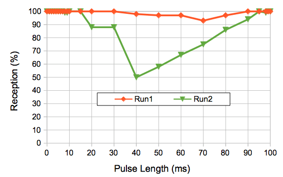
Figure: Reception versus Pulse Length for 10-Hz Stimulus and Head Fixture With Damaged Lamp Leads. Two tests with different arrangement of lamp leads outside the head fixture.
We have four stages of lamp artifact. In the first stage, the lamp artifact is less than 10 μV rms. The collar seals and lamp leads are intact. In the second stage, the artifact is less than 50 μV rms. The collar seals have been breached, but they are still tight. In the third stage, the artifact can be as large as 200 μV rms. The collar seals are loose, with a thick layer of fluid to conduct lamp current into the ground lead. In the fourth stage, the artifact can be as large as 2000 μV, reception can drop as low as 50%, and the lamp flashing is intermittent. One of the lamp leads is broken and current into the grounding spring has increased enough to disturb the data transmitter.
For stages one to three, lamp artifact for 10 ms flashes at 10 Hz is less than 50 μV. In stage four, the lamp is not flashing and data transmission is failing. The 2000-μV artifact in stage four is the least of our problems. We reach stage four only if we subject the lamp leads to so much fatigue that they break. Given that our leads survive implants of many months without breaking, we are hopeful that we will not reach stage four during implantation.
[25-SEP-17] We have E157.4 and E157.5 after one-hour burn-in and three-day soak. Noise in 37°C water is 7 μV. Switching noise is <1 μV. Reception 100% from each separately. With EEG leads out of water, we issue Stop commands and see loss of 10 continguous samples. With leads out of water or in water, command artifact is <10 μV. We measure frequency response by applying a 50-Ω sinusoidal sweep to the X leads. We do not attach a separate ground, see E157. Battery voltage of E157.4 is 4.0 V. Connect lamp leads to 13 V and see 100 mA flowing in, battery voltage is 4.1 V, after five minutes, get 4.2 V and disconnect. Battery voltage of E157.4 is 4.1 V, we charge up to 4.2 V. Outer dimensions of both devices: 10 × 22 × 33 = 7.0 ml box. The L− solder joints on both devices have corroded, but not those of L+, which is consistent with the leakage current of D3 and D4 flowing between the pins, with L− being the destination of electrons, where oxidation takes place. The same close-p of the leads shows how the glue between the lead and the collar reduces the width of the channel available for water. Here the gap appears to be 1/50th the diameter of the lead, and the lead is around 0.7 mm, so 14 μm wide.
[03-OCT-17] We have two methods for encapsulating the A3030E and its battery. Method 1 is dip in epoxy, ten-second run-off, rotate to cure, sand off excess on top and bottom, cover corners with SS-5001 silicone, dip three times in MED-6607 silicone. Dimensions are 32 mm × 21.5 mm × 9.6 mm. Displacement volume 5.3 ml. Method 2 is dip in epoxy, thirty-second run-off, rotate to cure. Repeat. Paint exposed parts with epoxy. Cover corners with SS-5001 silicone, dip three times in MED-6607 silicone. Dimensions are 32 mm × 21.3 mm × 8.7 mm. Displacement volume 4.5 ml. Method 2 produces a lumpy device. But with Method 1 we estimate 5% loss due to errors in sanding. Method 1 is the smaller volume. We have devices E157.3-7 encapsulated with Method 1. But E157.3 we sanded too far and damaged the battery, which bubbled for a while but still works. We will encapsulate E157.8-14 with Method 2.
[10-OCT-17] We have E157.6 and E157.7 after one week soaking in water. Both L− pins are corroded through and break off. The stainless steel helix is intact. We tin and clean. We confirm flashing, battery voltage, battery charging, frequency response, and reception. We top up the batteries to 4.2 V.
[13-OCT-17] We complete quality control on another nine A3030Es fully encapsulated. The frequency response of batch E157 is shown below.

Figure: Frequency Response of E157 Devices. We apply a 30-mV, 50-Ω sweep to the X input.
We check lamp stimulus. We top up batteries and measure battery voltage. All batteries in range 4.1±0.1 V. While testing batch E157 we find that command reception is 100% reliable for ranges 50 cm or less, and 100% reliable anywhere in an FE2F faraday enclosure. We place all devices in water with leads out of water to avoid corrosion of L− leads. In water together, they all respond to every command we issue to them within the confines of our faraday enclosure.
[12-JUN-18] We leave E157.14 flashing at 10 Hz with 1-ms pulses, starting 29-MAY and it is still flashing on 11-JUN, not flashing on 12-JUN, ran for 310-334 hours. Assuming battery current 55 mA while lamp is on, and 60 μA otherwise, we have average current 0.61 mA, so battery provided 195 mA-hr, which is close to its nominal capacity of 190 mA-hr. We did not re-charge it when we started. We cannot get it to respond to commands. We connect lamp leads to 5 V and see 10 mA flowing in. After about ten minutes, we are ablle to communicate with the device. It reports battery voltage 3.4 V and we get a low battery warning in the ISL Controller Tool. We charge the battery to 4.0 V and leave flashing again.
[04-JUL-18] Our E157.14 ran until at least 25-JUN-18, or 310 hours. We charge with 60 mA for one minute, set aside for 24 hours, and turn on data transmission. Battery voltage is 3.1 V.
[05-MAR-19] We prepare two blue and two white 3-mm LEDs with sockets to act as dummy head fixtures in up-coming trials of the A3030E at ION.
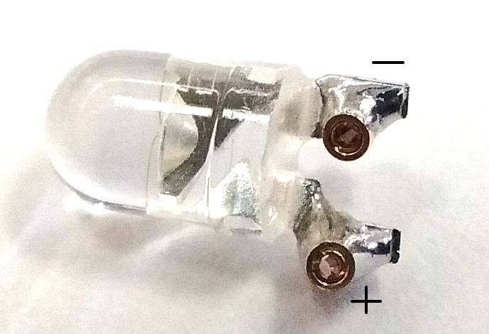
Figure: Dummy LED for Test of Grounding Spring. We are looking at the pin-entry side of two sockets. The positive terminal is the one with the socket on the outside of the LED lead. Connect the positive terminal to the orange ISL lead.
Devices C6.1 and D7.12 have inflated batteries and won't turn on. We discard them. Devices C6.7, D7.6, and D7.9 are fully functional. Device E157.14 won't turn on. It's battery voltage is low. We recharge and it works fine.
[13-JUN-19] At ION, we have two A3030E implanted with blue 3-mm LEDs buried in the dental cement of the head fixture. E157.13 has its EEG leads held in place on the skull by two plastic screws, while E157.8 has its leads held in place by steel screws. One day after surgery we turn on 10 ms pulses at 10 Hz and see 1-mV artifact in No8, and <10 μV artifact in No13. We record from No8 while flashing the LED and recording video. We obtain the files in Test_13JUN19 (150 MByte). The NDF metadata contains the following list of stimuli.
Measuring artifact in E157.8 implant.
200 s 1-ms 10 Hz 100% x100
260 s 2-ms 10 Hz 100% x100
300 s 5-ms 10 Hz 100% x100
340 s 10-ms 10 Hz 100% x100
380-400 s STOP commands
450 10-ms 10 Hz 0% x100
500 10-ms 10 Hz 20% x100
540 10-ms 10Hz 40% x100
580 10-ms 10 Hz 60% x100
620 10-ms 10 Hz 80% x100
650 10-ms 10 Hz 100% x100
690 10-ms 10 Hz 20% x100
800 100-ms 1 Hz 100% x10
850 50-ms 1 Hz 100% x10
880 20-ms 1 Hz 100% x10
950 10-ms 1 Hz 100%  x10
The following artifact is time 340-356 in the archive, when we turn on the lamp, flash at 10 Hz with 10-ms pulses, then stop. We notice no drop in reception during the lamp flashes, only during the transmission of the command that initiates the stimulus.
Figure: Lamp Artifact from E157.8. 100 flashes of 10 ms over 10 s.
When we turn down the lamp power to 0% we see no lamp flash artifact, but the initial and final switch-on pulses are present. These are caused by applying 5 V to the lamp leads after L+ has relaxed to 0 V and L− has risen to VB because of leakage through D3 and D4. With 100-ms flashes at 1 Hz, the lamp flash artifact is 3 mV. We check batteries of the six A3028E at ION, numbers 6, 7, 8, 9, 11, and 13. All are 3.8-3.9 V, except No6, which won't turn on.
[21-JUN-19] We recharge the battery in E157.6 and test the device with a white LED. It appears to function well and hold its charge. We set up No14 to flash a lamp at 10 Hz, 10-ms flashes, and fasten the EEG leads of No6 into some dental cement with screws.
Figure: Screws in Cement for Photovoltaic Effect.
We cover with water. We place the lamp directly over one screw, then the other, then half-way between. We are looking for light-induced artifact, but we see nothing. We add salt to the water. We see chemical artifact, which subsides, but no lamp artifact. With 50-ms flashes at 10 Hz, and the lamp directly over the X+ screw, we see in the spectrum of the X signal a sharp peak of 2 μV at 10 Hz. We move the lamp to shine in the saltwater 20 mm away and the peak disappears.
[08-NOV-19] We have been using Lattice Diamond LD2.11.0. We install LD3.11.0, select the LSE synthisis tool and recreate the P3030A project. We compile P3030E03 and re-program E157.1. We are using the Lattice Diamond Programmer 3.9.0 with TCK Divisor set to 2. Programming is unreliable with the divisor set to 1. Command reception, command acknowledgement, data transmission, and battery reporting all work well. Active current 80 μA is the sum of 60μA logic chip current, 9 μA inactive current, amplifiers, and ADC quiescent current.
[16-JAN-20] Device E157.8 returned from ION after months of implantation shows no sign of corrosion. Recharge battery. It receives commands easily. Response to 100-kΩ sweep correct. Leave flashing 10 ms at 10 Hz and transmitting X, in water.
[18-JAN-20] The water in which we left E157.8 has turned brown with rust. The positive lamp terminal is corroded. We remove and clean.