Implantable Stimulator-Sensor (A3037)
© 2020-2025 Kevan Hashemi,
Open Source Instruments Inc.
Contents
Notice of Obsolescence
Description
Versions
Design
Set-Up
Power Supplies
Stimulator Isolation
Calibration
Modifications
Development
Notice of Obsolescence
[27-JUL-22] The Implantable Sensor with Lamp (ISL) is obsolete. We have abandoned our attempts to combine sensor, stimulator, and light source into a single device. We instead separate stimulator and sensor into two devices: the Implantable Stimulator-Transponder (IST) and a Subcutaneous Transmitter (SCT). When equipped with an an Implantable Light-Emitting Diode (ILED), the IST becomes an optogenetic stimulator.
[19-MAY-24] We are retiring our Command Transmitter (A3029), replacing it with the command transmitters built into the Telemetry Control Box (TCB-B).
Description
[10-FEB-20] The Implantable Stimulator-Sensor (A3037) is a wireless electrical stimulator and biopotential sensor. It receives radio-frequency commands and transmits radio-frequency data messages. Its transmissions include biopotential samples, acknowledgements, and battery measurements. The displacement volume of the Mouse-Sized ISL (A3036A) will be no more than 1.3 ml. The electrical stimulus is delivered through two silicone-insulated helical wires terminated with miniature pins. A single radio-frequency command initiates an arbitrarily long stimulus. When combined with the A3036IL series of implantable lamps, the A3037 provides optogenetic stimulus. When combined with a bipolar depth electrode, the A3037 provides direct electrical stimulus.

Figure: The Implantable Stimulator-Sensor (A3037A). Volume 1.7 ml, mass 2.7 g. Leads by insulation color. Clear: transmit and receive antenna. Orange: positive stimulus. Purple: negative stimulus. Red: positive sensor input. Blue: negative sensor input.
The A3037 is powered by two separate batteries. One battery provides power to command reception, amplifiers, converters, and transmission circuits. The other provides the stimulus power. We call these the master and the stimulator circuits respectively. The master sends the stimulus control signal to the stimulator circuit by means of an isolator. The isolator makes sure there is no electrical connection between the two circuits at frequencies lower than 1 kHz. This isolation stops current flowing from the stimulator into the sensor amplifier, helping to eliminate stimulation artifacts.
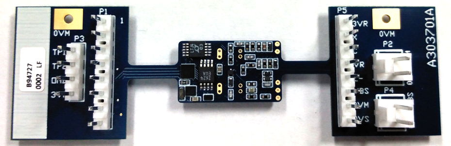
Figure: The A3037AV1 Fresh from Assembly House, Top Side. For bottom side see here. The central rectangle is the part that we use for the implant, and measures 20 mm × 12 mm.
The A3037A is equipped with two 10-mAhr lithium-polymer (LiPo) batteries, each 12 mm × 12 mm × 2 mm, one mounted to the top side of the circuit, the other mounted to the bottom side. We recharge the master and stimulus batteries simultaneously through the sensor and stimulator leads using a Dual Battery Charger (A3033C).
Acknowledgement: The Mouse-Sized Implantable Stimulator with Lamp (MS-ISL) development, which includes the Implantable Stimulator-Sensor (ISS), was funded by an SBIR grant from the NIMH.
Versions
The table below lists the existing versions of the Implantable Stimulator-Sensor (A3037).
| Version |
Master Battery
Capacity
(mA-hr) |
Stimulator Battery
Capacity
(mA-hr) |
Volume
(ml) |
Mass
(g) |
Lead Length (mm) |
Lead Resistance (Ω) |
Comment |
| A3037A |
10 |
10 |
1.7 |
2.7 |
45 |
56 |
Capacitive isolator |
| A3037B |
10 |
10 |
1.7 |
2.7 |
45 |
56 |
Optical isolator
|
Table: Versions of the Implantable Stimulator-Sensor (A3037).
The gold-plated pins on the end of the ISS's lamp leads mate with a pair of sockets on the A3036IL implantable lamps.
Design
The ISS is managed by a field-programmable gate array (FPGA) in a 2.5-mm square package, the XO2-1200. This device provides both volatile and non-volatile memory as well as thousands of programmable logic gates. It is capable of implementing arbitrarily-complex stimuli in response to a single command. The A3037A uses the same firmware as the Implantable Stimulator-Transponder (A3036), in which a single stimulus consists of a set number of pulses, each of fixed length, generated at regular intervales, or at random intervals with a known average value.
S3037A_1: ISS Version A Schematic, Page 1.
S3037A_2: ISS Version A Schematic, Page 2.
S3037B_1: ISS Version B Schematic, Page 1.
S3037B_2: ISS Version B Schematic, Page 2.
A303701A: Printed Circuit Board, Version A.
A303701A Panel: Panelized Printed Circuit Board, Version A.
A303701A_Top: Top View of A303701A PCB.
A303701A_Bottom: Bottom View of A303701A PCB.
A303701A_TO: Top Overlay of A303701A PCB, showing component locations.
A303701A_BO: Bottom Overlay of A303701A PCB, showing component locations.
Code: Logic Programs and Test Scripts.
Set-Up
The figure below shows how the stimulator-transponder system components are connected together. The stimulator-transponder system is an SCT system with the addition of a command transmitter and its antenna. Follow the SCT set-up instructions to set up the recording system for SCT biometric signals, then add the command transmitter as shown below.

Figure: ISS and SCT Connections for Optogenetic Experiments.
Referring to the diagram, we have the following components.
- The Neuroarchiver and Stimulator Tools run on the data acquisition computer.
- A local or global internet provides communication with the computer.
- The LWDAQ Driver provides power and communication with the data receiver and command transmitter.
- The driver and command transmitter both receive power from identical 24-V adaptors.
- The driver and command transmitter both receive power from identical 24-V adaptors.
- Shielded CAT-5 cables provide LWDAQ power and communication connections.
- The Octal Data Receiver picks up signals transmitted from the implanted ISLs.
- The Command Transmitter transmits radio-frequency commands to the implanted ISLs.
- The animals are housed in a faraday enclosure.
- The command transmit antenna is a loop antenna just like the receive antennas.
- The receive antennas are connected to coaxial cables.
- Dozens of animals may live together in the same faraday enclosure and be part of the same ISL system, each with their own implanted device, or with an implanted SCT that performs only EEG transmission.
- Feedthrough connectors allow use to bring cables into the faraday enclosure without allowing ambient noise and interference to enter.
- Coaxial cable carries radio frequency signals.
- BNC plugs and sockets.
- RJ-45 plugs and sockets.
The ISL system is compatible with the SCT system, in that we can implant ISLs and SCT in animals that live in the same enclosure, and receive signals from both. Only the ISLs will be able to respond to commands.
The Command Transmitter (A3029) plugs into a Long-Wire Data Acquisition (LWDAQ) system and also receives its own 24-V power input to boost its command transmission power. It acts as a LWDAQ device and transmits commands to implanted ISLs through a Loop Antenna (A3015C), the same type of antenna used to pick up data transmissions from implanted SCTs and ISLs.
The Data Receiver (A3027) plugs into the Long-Wire Data Acquisition (LWDAQ) Driver with Ethernet Interface (A2071). The (LWDAQ) system is a data acquisition system developed for high energy physics experiments and adapted here for neuroscience biopotential recording. The data receiver acts as a LWDAQ device. The LWDAQ Driver (A2037E) connects to the global Internet, your Local Area Network, or directly to your computer via an RJ-45 Ethernet socket. You communicate with the A2037E, and therefore the Data Receiver, via TCPIP. On the computer you use for data acquisition, you run the LWDAQ software, which you can download from here. In particular, you use the Receiver Instrument, the Neuroarchiver, and the Stimulator Tool.
The Stimulator Tool allows you to send Xon and Xoff commands to individual stimulators. These turn commands turn on the ISS sensor signal, which appears in the SCT recordings as a signal with the ISS's channel number, and records the biopotential connected to the ISL's sensor leads.
Power Supplies
[27-APR-20] The A3037 is equipped with two lithium-polymer batteries, one to provide power to the stimulator (B2), the other to provide power to the master circuit (B1). The master needs five power supplies. The 3VR supply is "3.0 V for Receiver". It is always on, and powers the radio receiver. The 3VM supply is "3.0 V for Master". It turns on only when the device is active, and provides power to the master's VCO (U9) and DAC (R18-R22). The VA supply provides power to the master's amplifier (U5) and ADC (U7). It is 3.0 V and turns on with 3VM. The 1V2 supply powers the master's logic chip (U8), and turns on only when the device is active. The VC supply is 1.2 V. It acts as the common or reference potential for the analog input, and turns on only when 1V2 turns on. To stimulator requires only one power supply: VBS, the stimulator battery voltage, which the stimulator connects directly to the stimulus leads L+ and L− when it receivers a 32-kHz square wave on ONL.
Most of the quiescent current used by the master while transmitting sensor data, running a stimulus, or processing sensor data is consumed by the logic chip through the 1.2-V power supply. We expect the logic chip, U8, to consume of order 200 μA from 1.2 V at animal body temperature. We create this power supply with a buck converter, so as to make efficient use of the energy stored in B1. The voltage provided by B1, which is VBM in the schematic, will start at around 4.2 V and drop to 3.5 V when the battery is exhausted.
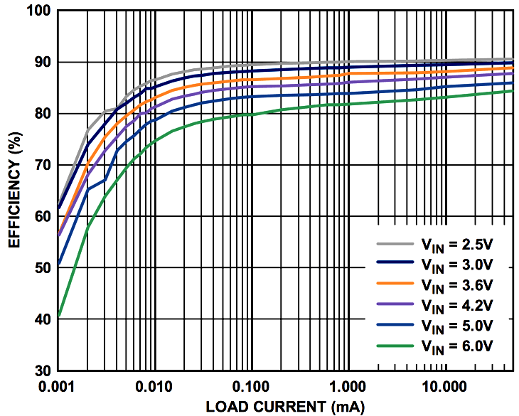
Figure: Conversion Efficiency of ADP5301 for Output 1.2 V. A figure taken from the ADP5301 data sheet.
The ADP5301 converts 3.6 V to 1.2 V at 200 μA with efficiency 87%. A 200 μA 1.2-V current will draw 200 μA ÷ 0.87 × 1.2 ÷ 3.6 = 77 μA from the battery. We operate the ADP5301 in its hysteresis mode, for which ripple is around 40 mVpp at 1 kHz for 200 μA load current. To create VC, the analog reference voltage, we pass 1V2 through 1 kΩ with 10 μF to 0V. We expect ripple of order 1 mV on VC at 1 kHz, which will subtract from sensor voltage X. The low-pass filter attenuates 1 kHz by at least 40 dB. We expect no more than 10 μVpp of noise showing up on X due to ripple on 1V2.
The radio receiver is always powered. When VR exceeds the threshold TH, comparator U4 asserts RP, which causes U6 to turn on 3VM. We use 3VM to turn on the ADP5301 (U1) through its enable pin. It takes 2 ms for U1 to start up. This adds to the power-up delay of U8, which is around 3 ms, to give us 5 ms before U8 can respond to commands encoded on RP. Our command transmission protocol specifies an initial pulse of at least 5 ms to allow U8 to assert OND.
The ADP5301 uses a 2.2-μH inductor to convert 3.6 V to 1.2 V. The data sheet recommends a P0805 part with saturation current 600 mA and resistance 170 mΩ. We are short of space and planning on using the converter at currents less than 1 mA, so we select a P0603 inductor, the MBKK1608T2R2M. It's saturation current is 580 mA and resistance 345 mΩ.
Stimulator Isolation
[15-FEB-20] When the MS-ISL is implanted in an animal, its L+ and L− leads terminate with pins plugged into an implantable lamp. If the insulation applied around the pins were perfect, no current can flow from the lamp pins into the animal body. Despite our best efforts, however, we have been unable to devise reliable insulation for the lamp pins. Electrical contact between the lamp pins and the animal body can cause substantial lamp artifact in our sensor signal. Current can travel from the lamp pins to the sensor electrodes, generating an electric field in the animal body that corrupts the biopotential we are trying to monitor. One way to eliminate this artifact is to isolate the the sensor and stimulator, as we did by implanting an ISL (A3030E) and an SCT (A3028D) in the same animal. The ISL provided lamp power, the SCT provided EEG monitoring. We saw no sign of lamp artifact in the EEG even after two months of implantation.

Figure: Lamp Current Flowing For Isolated Stimulator and Sensor Circuits. This arrangement of two separate implants proved successful in eliminating lamp artifact. The A3037 is equipped with two batteries and an isolator in order to achieve the same effect.
The MS-ISL is equipped with two batteries. The master circuit communicates with the stimulator through an isolator. The only connection between the two circuits is a 50-pF capacitance between their 0-V potentials. When the stimulator turns on the lamp, the average voltage on the lamp pins drops by 1.8 V with respect to the stimulator 0-V potential, which means the stimulator 0-V potential must drop by 1.8 V with respect to the animal body. We estimate the capacitance between the stimulator and the animal body is dominated by the capacitance of its two stimulus leads. Assuming 50-mm leads, their combined capacitance is 100 pF. Assuming a lead resistance of 25 Ω, the time constant of this charging will be 2.5 ns, which is negligible compared to our shortest sample period.
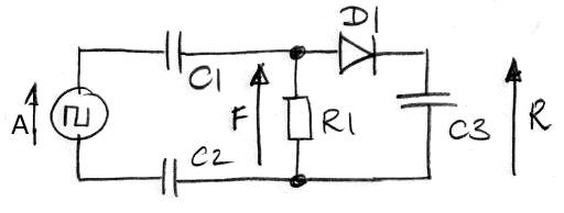
Figure: Capacitor-Isolation Test Circuit. We have: applied voltage X, feedthrough voltage F, and rectified voltage R. Components are isolation capacitors C1 and C2, load resistor R1, rectifier D1, and balast capacitor C3.
Meanwhile, the X− lead of the MS-ISL master circuit is connected to the body by a wire and a reference electrode of impedance <10 kΩ. When the stimulator 0-V drops by 2 V with respect the animal body, the 50-pF isolation capacitance will pull the master 0-V potential down by 2 V as well. The 50-pF isolation capacitance then charges through the X− lead its electrode until the 0-V potential of the master is restored to its usual level. Its usual level is 1.2 V below the potential of the animal body, this being the VCOM potential of the X− electrode. Assuming a reference electrode of impedance <10 kΩ, this charging will take 500 ns, which is negligible compared our shortest sample period.
Calibration
Preparing an A3037 for encapsulation is similar to preparing a Subcutaneous Transmitter (A3028) for encapsulation, with the added steps of tuning the antenna matching network, and the added burden of a two-minute firmware compile time and thirty-second logic chip programming time. The first thing we do is prepare the board for tuning. Attach an antenna to the circuit so we can tune its matching network. Solder a thin, 50-mm insulated wire to the antenna pad. We need to apply power to the circuit so that its antenna switch will connect the antenna to the matching network. Connect a LiPo battery to the VBM plug.
We tune the antenna matching network with a 870-960 MHz sweep generated by a Modulating Transmitter (A3014MT). We take the sweep signal and split it in two. One part we mix with 910 MHz to produce a ±45 MHz intermediate frequency, which we pass through a 21-MHz low-pass filter and view on an oscilloscope. The second part we connect to an 800-1000 MHz amplifier. We use a modified A3029B, which produces a 10-dBm sweep. We connect the 10-dB sweep to an A3015C loop antenna. We place the A3037 with battery on the loop antenna and measure VR at P5-4 with a ×1 probe. We must have the battery attached so the RF switch U4 is powered up, connecting the antenna to the matching network. We will see a sweep something like this. With favorable orientation of the antennas, the peak should be around 80 mV high, and somewhere within the range 900-930 MHz. If it is higher than 915 MHz, we increase C19 by 0.1 pF. If lower than 905 MHz, we decrease C19 by 0.1 pF. We wash and dry the board, then repeat our measurement and perform further adjustments until the peak response lies in the range 905-915 MHz.
Now that the antenna matching network is tuned, we move on to programming, calibration and current consumption measurement. We start by measuring the inactive current consumption. Connect a 3.7 V power supply to the programming extension through an ammeter. Measure the current consumption of the circuit. This current is the inactive current. Acceptable values are 6-9 μA.
Now we program the logic chip on the A3037 with a default configuration. Connect a Lattice Semiconductor programming cable to P1. Connect a jumper between the OND and 3VR pins of P3. This jumper activates the board by turning on power to the logic chip. Change the range of the ammeter to 200 mA. A lower ammeter range will stop the short burst of 30 mA drawn from the battery during programming. Open the Lattice Diamond Programmer. Program the board with firmware P3037A_65_19_5. The circuit has now been configured with the following constants, as presented in the VHDL source code, which we will soon edit as part of our calibration and configuration procedure.
-- Configuration and Calibration Constants.
	constant device_id : integer := 65; -- The identifier number for this device
	constant fck_calib : integer := 19; -- Calibration of ring oscillator to give 10 MHz on FCK
	constant frequency_low : integer := 5; -- Low frequency code for data transmission.

-- Stable Calibration Constants
	constant frequency_step : integer := 1; -- High minus low frequency code
	constant sample_rate : integer := 512; -- How often we transmit diagnostic signal
Knowing the initial configuration values allows us to estimate the correct values after we measure the behavior of the circuit. To configure and calibrate the circuit, we follow the steps listed below. We record the final values of all current consumptions and calibration constants in a table on the back of the batch production record sheet.
- Disconnect the programming cable from the A3037. Remove the jumper from P1 that activates the board.
- Set up a Command Transmitter (A3029C) and Loop Antenna (A3015C). Open the Stimulator Tool in the LWDAQ Software and configure it to use the command transmitter and control a device with the default id given above.
- Open the Lattice Diamond Compiler and open the P3036 project. Open the main VHDL file. It will have a name like P3037A02_Main.vhd. Locate the above lines. These are the lines we will edit.
- Use the Stimulator Tool to turn on transmission of the A3037 data signal with the Xon button. We know the circuit's id because we set it with the initial program, shown above. Measure the spectrum of the A3037 transmit signal using a Loop Antenna (A3015C) connected to a Spectrometer (A3008C). The peak of the spectrum should lie in the range 913-918 MHz. If the peak is too high, reduce frequency_low in the VHDL file. If too low, increase frequency_low.
- We must calibrate the logic chip's ring oscillator. Put an oscilloscope probe on TP1, which is pin P3-1 on the programming extension, and presents us with the FCK (Fast ClocK) signal. We want FCK to be a 10-MHz square wave. If its period is greater than 110 ns, reduce fck_calib. If its period is less than 95 ns, increase fck_calib.
- Turn off the data signal with the Stimulator Tool Xoff button. The FCK signal on TP1 should disappear.
- Set the device_id in the VHDL code to the value we want for this circuit. If we want the data signal to have some frequency other than the default 512 SPS, we set it so some other power of two samples per second now. Compile the code. The compilation will take a couple of minutes.
- Connect the programming cable to the programming extension. Activate the board by connecting a jumper across OND and 3VR on P3. The ammeter will report current of 3-4 mA. Make sure the ammeter is set to a range of 200 mA to support programming. Press the Program button in the Lattice Diamond Compiler and use the programing panel to program the logic chip with the new firmware. Programming will take less than a minute.
- Repeat our measurements of transmit spectrum and transmit clock frequencies, adjust VHDL program, and re-program logic chip until both frequencies are correct. Remove the jumper from P3. Remove the programming connector.
- Turn on transmission of the A3037 data signal with the Xon button in the Stimulator Tool. Check that the data signal is being transmitted using a Loop Antenna (A3015C) connected to an Octal Data Receiver (A3027). Set the ammeter range to 200 μA and measure current consumption. We call this measurement the transmit current. Acceptable values for 512 SPS are 100-150 μA.
- Start a stimulus consisting of a large number of 10-ms flashes every 1000 ms with the Start button. Turn off signal transmission with Xoff. By starting the stimulus and then turning off transmission, you do not have to switch the ammeter to a higher range, because the board is powered up the entire time. The board needs 20 mA ony when it wakes up from its inactive state. Measure current consumption during the stimulus. This measurement is the active current. Acceptable values are 50-70 μA. No light will flash because we have no light attached to the circuit board.
Assuming the currents and frequencies are within their acceptable ranges, the board is now ready to for its batteries and leads, and after that we have quality assurance to check all the above measurements again.
Modifications
To convert the A3037A into A3037B built on the A303701A circuit board, we do the following.
- Remove C15 and C15.
- Replace R14 with 100 kΩ.
- Replace D5 with 0 Ω.
- Solder 100 kΩ P0402 resistor R25 to ONL pad of C15 footprint, leaving other end free.
- Solder wire to free end of R25, Wire 1.
- Solder wire to the 0VM pad of C16 footprint, Wire 2.
- Solder wire to top end of D5 footprint, Wire 3.
- Solder wire to VBS contact on top side of board, Wire 4.
- Place U11, CTP17 upside-down (green side up with pin one dot) over C15 and D5 footprints on top side of board.
- Solder Wire 1 to U11-1, Wire 2 to U11-2, Wire 3 to U11-3 and Wire 4 to U11-4, as shown in this photo.
The U11 modification eliminates the capacitive isolator and replaces it with an optoisolator. The result is elimination of all lamp artifact except for edge noise, which has zero average value. To the A303701A we will make the following modifications for the A3037B.
- Correct labelling of P5, which has VBS and L− reversed.
- Replace capacitive isolator with optoisolator. Remove C15, C16, D5. Add optoisolator and a resistor in series with its LED.
Development
Winter-20
[11-FEB-20] We try out the LTV355T optoisolator. We apply a square wave drive current to the LED through a resistor R1, connect the collector directly to 3.7 V, and connect the emitter through a resistor R2 to 0 V. In one test, we have a capacitor C1 = 56 pF in parallel with R2 to mimic the gate capacitance of a lamp-switching mosfet.
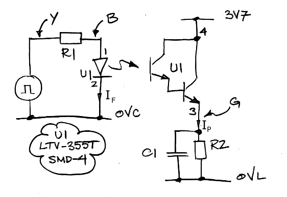
Figure: LTV355T Optoisolator Test Circuit. Square wave drive voltage Y, LED voltage B, and photodarlington emitter voltage G, are named after the colors we use to display them on our oscilloscope.
With Y = 2.0 V and R1 = 10 kΩ we see B = 1.0 V, which implies IF = 100 μA. With R2 = 1 kΩ, G rises to 3.0 V. When we add a 56 pF capacitor in parallel with the load resistor and the rise and fall times are unaffected.
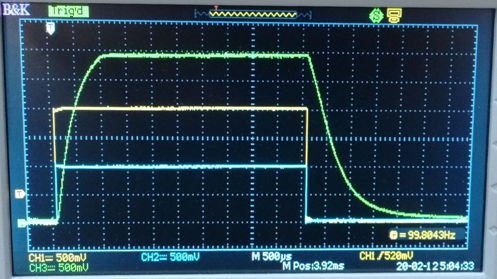
Figure: LTV355T Switching Signal. Yellow: Y, Blue: B, Green: G, for R1 = 10 kΩ, R2 = 1 kΩ.
We vary R1, R2, and Y to obtain the following table of rise and fall times, as well as the emitter voltages attained by the photocurrent running through R1.
Drive Current
(μA) |
B
(V) |
R2
(kΩ) |
Rise Time
(ms) |
Fall Time
(ms) |
| 40 | 3.0 | 100 | 2 | 100 |
| 40 | 3.0 | 10 | 2 | 10 |
| 40 | 1.2 | 1 | 1 | 1 |
| 100 | 3.0 | 1 | 0.5 | 1 |
| 120 | 3.0 | 1 | 0.5 | 1 |
| 200 | 3.0 | 1 | 0.2 | 0.5 |
Table: Optoisolator Performance. We give approximate 10-90% rise and fall times. Voltage B is photodarlington emitter voltage, R2 is photodarlington emitter resistor.
With IF = 40 μA, G = 1.2 V, so IP = 1.2 mA and IP/IF = 30 = 3000%. Looking at Fig 5 of the LTV355T data sheet, Current Transfer Ratio versus Forward Current, we expect CTR increasing from 1000% at 100 μA to 4000% at 700 μA. And yet we see 3000% at 40 μA. The data sheet gives minimum and maximum values of CTR at IF = 1 mA of 600% and 7500%.
If we power the LED with an ML1220 battery, the battery's source resistance will be roughly 40 Ω and its voltage will be roughly 2.5 V, creating a power supply we shall call 2V5. A 100 μA LED drive current will drop 2V5 by 4 mV. Assuming an amplifier gain of 100 and average amplifier output 1.2 V, a 4 mV drop in 2V5 will cause a 40 mV ÷ 100 ÷ 2 = 20 μV rise in the apparent sensor voltage. This rise will be further attenuated by a 1 kΩ resistor and 10 μF capacitor we use to filter 2V5 into the analog supply voltage VA, for a time constant of 10 ms.
[13-FEB-20] Another way to isolate the master and stimulator circuits is with capacitors. We build the following circuit with the help of a 1N34A germanium diode.
Figure: Capacitive Isolator, Version One (CIV1). We have: applied voltage A, feedthrough voltage F, and rectified voltage R. Components are isolation capacitors C1 and C2, load resistor R1, rectifier D1, and balast capacitor C3.
We apply a 0.0-2.5 V square wave to A using a function generator. We measure R with a battery-powered multimeter so we do not compromise our isolation with measurement grounds. We vary the frequency of the square wave.
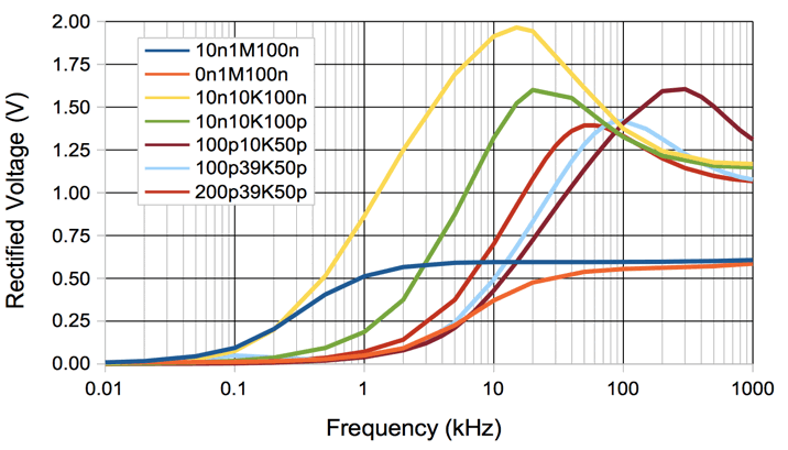
Figure: Rectified Voltage vs Frequency. Blue: C1 = C2 = 10 nF, R1 = 1.0 MΩ, C3 = 100 nF. Orange: C1 = 10 nF, C2 = 0.0 nF, R1 = 1.0 MΩ, C3 = 100 nF. Yellow: C1 = C2 = 10 nF, R1 = 10 kΩ, C3 = 100 nF. Green: C1 = C2 = 10 nF, R1 = 10 kΩ, C3 = 100 pF. Brown: C1 = C2 = 100 pF, R1 = 10 kΩ, C3 = 50 pF. Cyan: C1 = C2 = 100 pF, R1 = 39 kΩ, C3 = 50 pF. Red: C1 = C2 = 200 pF, R1 = 39 kΩ, C3 = 50 pF
With R1 = 1 MΩ, C1 = 10 nF, and C3 = 100 nF, we modulate a 32-kHz square wave so as to view the rise and fall time of R. We must short C2 with our oscilloscope probe ground clips in order to view R.
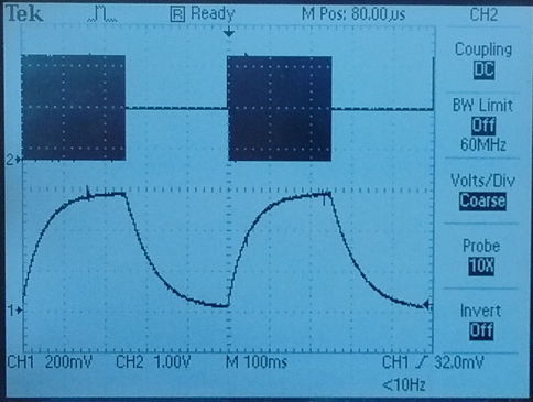
Figure: Capacitor-Isolated Voltage Transfer. Top: A, an amplitude-modulated, 32-kHz square wave. Bottom: R. We have C1 = 10 nF, C2 shorted by ground clips, C3 = 100 nF, R1 = 1.0 MΩ.
The 100-ms rise and fall times are consistent with R1C3 = 1.0 MΩ × 100 nF. We drop R1 from 1 MΩ to 10 kΩ and repeat the same measurement with a 32-kHz, modulated square wave.
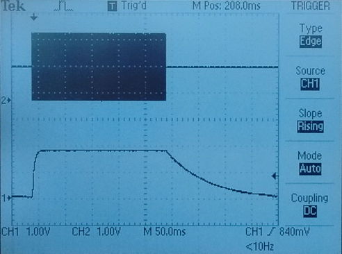
Figure: Capacitor-Isolated Voltage Transfer. Top: A, an amplitude-modulated, 32-kHz square wave. Bottom: R. We have C1 = 10 nF, C2 shorted by ground clips, C3 = 100 nF, R1 = 10 kΩ.
The rise time of 1 ms is consistent with R1C3 = 10 kΩ × 100 nF = 1 ms. The falling slope of 1.0 V in 50 ms is consistent with D1 draining C3 at 2 μA. The 1N34A data sheet gives saturation current 5 μA. With a continuous 32-kHz square wave, we look at F. We must short C2 with our ground clips in order to make this observation. But we confirm with our isolated meter that F has average value zero when capacitor C2 is not shorted.
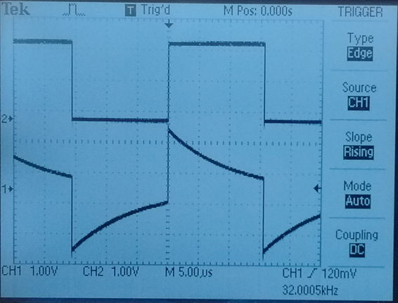
Figure: Capacitor-Isolated Voltage Transfer. Top: A, a 32-kHz square wave. Bottom: F. We have C1 = 10 nF, C2 shorted by ground clips, C3 = 100 nF, R1 = 10 kΩ.
We reduce C3 to 100 pF and keep R1 = 10 kΩ. We are shorting C2 with our oscilloscope ground clips, but we the rectified voltage still rises to 1.5 V, which matches our isolated measurement with battery-powered multimeter. We apply modulated 32-kHz to A.
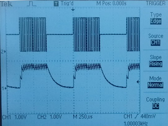
Figure: Capacitor-Isolated Voltage Transfer. Top: A, an amplitude-modulated, 32-kHz square wave. Bottom: R. We have C1 = 10 nF, C2 shorted by ground clips, C3 = 100 pF, R1 = 10 kΩ.
We previously had the balast capacitor much greater than the isolating capacitors. Now we have the balast capacitor much smaller than the isolating capacitors. The rising slope of R is 1.0 V in 10 μs, which is consistent with C3 = 100 pF being charged by a forward-biaset D1 with 10 μA. The falling slope of 1.0 V in 200 μs is consistent with a reverse-biased D1 draining C3 = 100 pF at 2 μA.
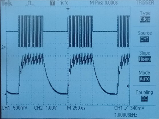
Figure: Capacitor-Isolated Voltage Transfer. Top: A, an amplitude-modulated, 32-kHz square wave. Bottom: R. We have C1 = 100 pF, C2 shorted by ground clips, C3 = 100 pF, R1 = 10 kΩ.
[14-FEB-20] With C1 = C3 = 100 pF, C2 shorted, and R1 = 10 kΩ, R has rises to 1.3 V, which is half the amplitude of A. We try C1 = C2 = C3 = 100 pF and R1 = 10 kΩ, with the addition of a 1 kΩ current sense resistor in series with the function generator return. At 32 kHz we have R = 1.02 V. The voltage across the current sense resistor is a sequence of alternating spikes 30 mV rms and average value within 500 μV of zero. We increase frequency to 200 kHz to obtain a better view of the spikes, which are now 60 mV rms, implying current 60 μA rms. The time constant of the spikes is consistent with R1 = 10 kΩ charging C3 = 100 pF, which is 1 μs.
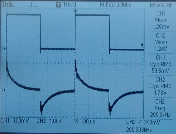
Figure: Input Current Spikes. Top: A, a 200-kHz square wave. Bottom: Voltage across 1-kΩ sense resistor. We have C1 = C2 = C3 = 100 pF and R1 = 10 kΩ.
We return to 32 kHz. We have C1 = C2 = C3 = 100 pF and R1 = 10 kΩ plus a 1-kΩ sense resistor. We measure R = 1.02 V with our battery-powered meter, and current 30 μA rms. We remove R1 and R = 0.00 V. We try C1 = C2 = 10 pF, C3 = 100 pF, and R1 = 10 kΩ and get R = 0.25 V and current 6 μV rms. We remove R1 and get R = 0.00 V
The load resistor's function is to discharge the isolation capacitors. On the rising edge of A, 2.5 V appears across the load resistor, and the isolation capacitors charge until they each have 1.25 V across them. During the brief charging period, the diode charges the balast capacitor to 1.25 V. After that, the diode is reverse-biased by roughly 1 V and discharges the balast capacitor slowly. On the falling edge of A, the load resistor discharges the isolation capacitors. The diode continues to discharge the balast capacitor slowly, but the rectified voltage has dropped by only 0.4 V by the time the next rising edge occurs. On the rising edge, because the isolation capacitors are discharged, they now generate a positive feedthrough voltage, which raises the rectified voltage back up to 1.25 V. The result is an average rectified voltage of 1.0 V.
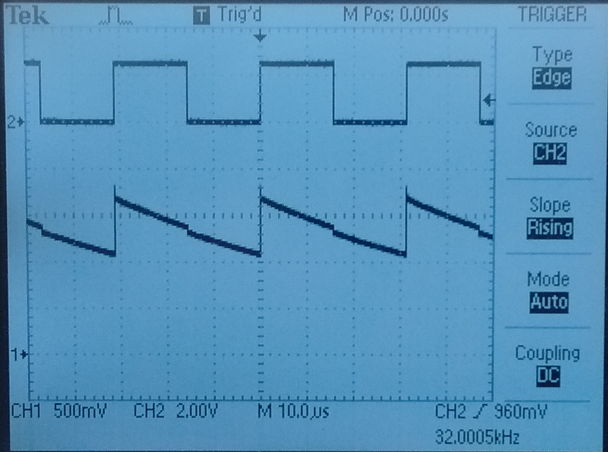
Figure: Capacitor-Isolated Voltage Transfer. Top: A, 32-kHz square wave. Bottom: R. We have C1 = 100 pF, C2 shorted by ground clips, C3 = 50 pF, R1 = 39 kΩ..
If we remove the load resistor, the rectification fails. After enough positive cycles of the square wave, the isolation capacitors have charged up to 1.25 V each, due to current through the diode and the 10 MΩ impedance of our meter. They do not discharge on the negative cycles because the diode inhibits current in the discharge direction. On the positive halves of the square wave, the feedthrough voltage is zero. On the negative halves, the feed through voltage is −2.5 V. The balast capacitor does not discharge to a negative voltage because the diode is reverse-biased.
With C1 = C2 = C3 = 100 pF and R1 = 10 kΩ, each time the 2.5-V square wave transitions, our current sense resistor reports that 125 pC of charge moves in or out of the capacitors. If we deliver the square wave with a logic output, the logic chip power supply will deliver 125 pC on each rising edge, and the logic chip output will drain 125 pC on each falling edge. At 32 kHz, the current drawn from the power supply will be 125 pC × 32 kHz = 4 μA. For this current, we get 1.0 V on C3 = 100 pF, which is sufficient to turn on the DMG1024UV mosfet we use to switch the lamp power in the A3036 stimulator. That mosfet's gate capacitance is 60 pF. We predict that R for 60 pF will be 100 ÷ 60 × 1.0 V = 1.7 V. The rise and fall time of the gate voltage in response to turning on and off the 32 kHz square wave will be around 100 μs and 200 μs respectively, fast enough to generate 500-μs flashes of light.
Our capacitive isolator delivers five times faster response than our opto-isolator, but at 4% of the battery current consumption. It's board area is four P0402 components (for the diode we can use the SMS7630-040LF), or 7 mm2. The opto-isolator alone is 29 mm2. Of course, the optoisolator offers complete isolation between the two circuits, while the connection between the 0-V potential of the A and R circuits in our capacitive isolator is two 100 pF in series, or 50 pF. But our calculations suggest that this 50 pF is insignificant.
[17-FEB-20] We try C1 = C2 = 100 pF, R1 = 10 kΩ, and C3 = 50 pF and plot frequency response of R. We try R1 = 39 kΩ and repeat. The figure below shows R with C2 shorted. Rise and fall times of order 100 μs, see here. With continuous 32 kHz, the voltage R is shown below, droops by 500 mV, but is never less than 1.1 V. When C2 is not shorted, we presume that the voltage droops by 500 mV, its average is 1.1 V, which means its minimum will be 0.85 V, which is is not sufficient to guarantee that our DMG1024UV will turn on.
We try C1 = C2 = 200 pF, R1 = 39 kΩ, and C3 = 50 pF. At 32 kHz R measured with our DVM is 1.27 V and achieves a maximum at 60 kHz. We plot R versus frequency. This arrangement is sufficient to turn on our mosfet at a cost of 8 μA. For modulated 32 kHz, rise and fall times are 100 μs and 250 μs respectively, as shown below.
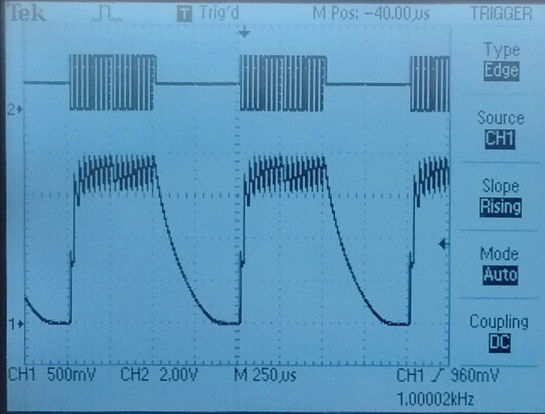
Figure: Capacitor-Isolated Voltage Transfer. Top: A, an amplitude-modulated, 32-kHz square wave. Bottom: R. We have C1 = 200 pF, C2 shorted by ground clips, C3 = 50 pF, R1 = 39 kΩ..
[18-FEB-20] We assemble an isolator out of SMT components mounted on SIP adaptors. Our C1 = C2 = 200 pF in P0402, our R1 is 50 kΩ in P0402. Our D1 is SMS7621-079LF, and Q1 is the ZVN3306F in SOT-23, connected to an axial resistor and radial white LED. We are using the gate capacitance of Q1 in place of C3. This capacitance is typically 35 pF.
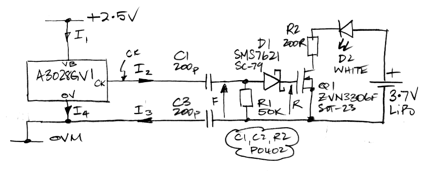
Figure: Capacitor Isolator, Version Two (CIV2) Schematic. We measure I1. We have I2 = I3, average values of I2 and I3 are zero, and I1 + I2 = I3 + I4.
We produce the 32 kHz, 2.5-V square wave with an A3028GV1 powered by 2.5 V. With CK disconnected, I1 = 92.3μA. We connect CK to the isolator and I1 = 98.9 μA, making isolator current 6.6 μA. The LED turns on. Voltage R is 2.0±0.2 V. Our diode is the SMS7621-079 power detector. We started with the SMS7630-079 zero-bias diode, but its resistance with zero bias is too low, and it discharges the gate capacitance too quickly even when reverse-biased by 1 V.
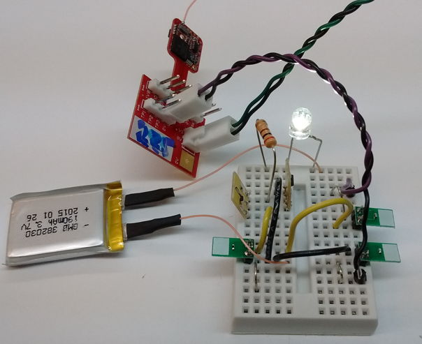
Figure: Capacitive Isolator, Version Two (CIV2). We have C1 = C2 = 200 pF, R1 = 50 kΩ, D1 = SMS7621-079LF, all mounted on SIP adaptor boards. A LiPo battery powers the lamp. The 32 kHz is delivered by an SCT circuit.
We supply CK now with our function generator and modulate at 1 kHz. We short C2 with our probe grounds so we can look at CK, F, and R at the same time.
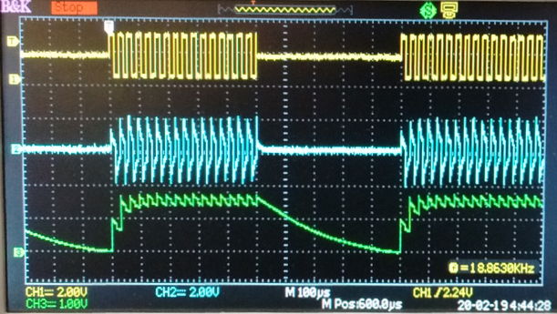
Figure: Capacitive Isolation. Showing CK (Yellow), F (Blue), and R (Green). We have C1 = 200 pF, C2 shorted by probe grounds, R1 = 50 kΩ, D1 = SMS7621-079LF.
Rise time from 0.0 V to 1.2 V is 50 μs, and fall time from 1.5 V down to 0.5 V is 200 μs. The DMG1024UV, if we choose to use it in the A3037, has gate capacitance 60 pF and threshold somewhere between 0.5 and 1.0 V.
[24-FEB-20] We place an A3028E-AA SCT in a 500-ml beaker of water with an A3036A IST connected to an A3036IL-A implantable lamp. The SCT's X electrodes are 10 mm apart on the far side of the beaker from the L contacts on the lamp. We flash the lamp at 10 Hz for 10 ms. Artifact on the SCT input is 600μV negative pulses of 10 ms. We cover the lamp with gaffer's tape. Water can pass in and out of the tape wrapper. Artifact is 50 μV positive pulses of 10 ms. We exchange the locations of the X electrodes. Artifact is 40 μV negative pulses of 10 ms. We remove tape and separate the X electrodes by the diameter of the beaker. Artifact is 20-mV positive spikes of 10 ms. We remove SCT from water, hold electrodes in hands and observe heartbeat.
Spring-20
[07-APR-20] We build the following isolator, in which we produce A drive signal with two 2.7-V logic signals CK1 and CK2 provided by a re-purposed A3028 circuit powered by a 2.7-V battery. We measure the A3028 quiescent current with an ammeter, but the drive circuit is otherwise floating.
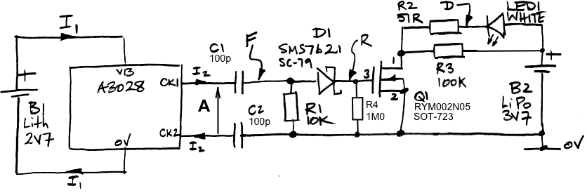
Figure: Capacitor Isolator with Floating Drive Circuit. We measure I1, F, R, and D.
Resistor R3 will be present in the A3037 to ensure the leakage current of Q1 does not apply a voltage across the lamp electrodes. Resistor R1 models the resistance of the A3037 stimulus leads. The RYM002N05 has typical input capacitance 40 pF at drain-source voltage 0V, and gate threshold voltage 0.3-0.8 V. Resistor R4 reduces the LED turn-off time.
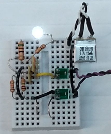
Figure: Capacitive Isolator, Version Three (CIV3). A miniature LiPo battery powers the LED. The 32 kHz is delivered through the twisted pair cable on the right side.
We modulate A at 512 Hz, turning on the square wave for 500-μs bursts. We measure F, R, and D with ×10 probes. When we attach a probe to F we see a slight decrease in the average value of R, but we ignore this decrease when measuring R.
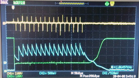
Figure: Capacitive Isolator Signals for R4 = 1 MΩ. Showing F (Yellow), R (Blue), and D (Green). We have C1 = C2 = 100 pF, CK1 is 3-V modulated square wave, CK2 is 0V.
Turn-on time is 50 ns, turn-off time is 100 μs. The average value of R rises to 1.3 V. The descending slope of the sawtooth on R is 700 mV ÷ 30 μs = 23 V/ms, suggesting a discharge time constant of 1.5 V ÷ 23 V/ms = 65 μs. We expect 1 MΩ × 40 pF = 40 μs. When we turn the LED on continuously, I1 increases by 8 μA. Battery B2 voltage is 4.0V. The drain of Q1 drops to 50 mV when the LED is on, which implies drain-source resistance of 50 mV × 50 Ω ÷ 1000 mV = 2.5 Ω. We set CK2 = !CK1 and R rises to 2.5 V, but I1 increases by 25 μA with continuous drive.
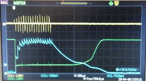
Figure: Capacitive Isolator Signals for R4 Omitted. Showing F (Yellow), and R (Blue), and D (Green). We have C1 = C2 = 100 pF, CK1 is 3-V modulated square wave, CK2 is 0V.
Without R4, the average value of R rises to 2 V. Turn-on time is 50 ns, turn-off time is 500 μs. With the LED on continuously, I1 increases by 9 μA. With CK2 = !CK1, R reaches 3.5 V.
[08-APR-20] With our oscilloscope probes grounded on the 0V of the LED drive circuit, we apply a 3-kHz, 4-Vpp square wave to 0V on the A3028 circuit. We turn off the drive signal by connecting CK1 to HI and CK2 to LO. The LED turns on.
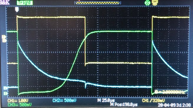
Figure: Capacitive Isolator Signals with Square Wave Offset Voltage. Showing 0V of A3028 (Yellow), R (Blue), and D (Green). We have R4 = 1 MΩ.
We reduce the amplitude of the square wave. The LED turns off at 1.2 Vpp. When we switch to a 4-Vpp sine wave, the LED stays off for frequencies less than 43 kHz, and turns on for higher frequencies. We go back to 3 kHz 4-Vpp sine wave. We enable the modulated drive signal on CK1, with CK2 = LO. We disconnect CK1. The LED turns off. We restore CK1 and disconnect CK2. The LED remains just as bright. We remove the offset voltage. We disconnect CK1 and CK2 in turn and confirm that both must be connected for the LED to turn on.
[23-APR-20] Schematic complete, working on A303701A layout. The figure below shows the pinout of the logic chip WLCSP-25 package. We end up using all 25 pins on the chip. The board has two extensions. One for programming and logic test points. The other for external battery connection, lamp voltages, isolator voltages, applying analog input, and tuning the crystal radio.
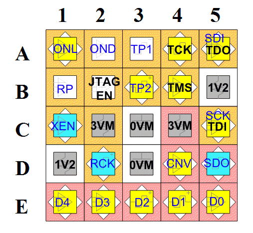
Figure: Pinout of Logic Chip WLCSP-25. D1, B5 are VCC = 1.2V. C2, C4 are VCCIO = 3VM = 3.0V. C3, D3 are 0VM = 0V. B2 is JTAGEN, dedicated programming port enable. C5, A5, B4, A4 are TDI, TDO, TMS, and TCK programming port signals when JTAGEN asserted, general-purpose I/O otherwise. All other pins general-purpose I/O. Signal names marked in blue.
[04-JUN-20] A few weeks ago we received samples of CTP17 from CT Micro, a "DC 4-Pin DFN Phototransistor Optocoupler". We place a 10-kΩ resistor in series with the LED. We apply a square wave 0 V to X, where X we increase from 0V to 10V, to the resistor and LED. We put a 1-kΩ resistor in series with the photodetector and connect to 9V. We measure the voltage across the 1-kΩ resistor to obtain the photodetector current. After consulting the data sheet, we obtain the LED current by assuming a forward voltage of 1.2 V. We divide the photocurrent by the LED current to obtain the current transfer ratio (CTR).
| LED Current (mA) | CTF (%) |
| 0.18 | 500 |
| 0.28 | 430 |
| 0.38 | 400 |
| 0.88 | 300 |
Table: Current Transfer Ratio versus LED Current for CTP17 Opto-isolator.
We find the rise and fall times of the photocurrent are 10 μs, compared to 1 ms in an earlier experiment. In this case, we have a minimum of 6 V across the photodetector, so it does not saturate. If we use 3.6V for the photodetector circuit, and allow 2 V for the photodetector, we can use a 100 kΩ load to apply 1.6 V to the base of a mosfet. The photocurrent would be 16 μA. Our test does not tell us what the LED current would have to be for 16 μA photocurrent, but could be as low as 10 μA, making the CTP17 competitive with our capacitive isolator. Despite being the smallest opto-isolator in the world, the CTP17 is still larger than our capacitive isolator.
Summer-20
[23-JUN-20] We have three A3037AV1 assemblies. We connect a LiPo battery to P2 so as to provide VBM. We jumper OND to 3VR so as to turn on power to the logic chip. We program the logic chip with P3037A01, which has all functionality implemented except for digitization and transmission of sensor data. We attach a 50-mm wire antenna and look at the response of the crystal radio to a 10-dBm sweep 860-970 MHz. These boards are loaded with C5=1.0pF, C6=1.0pF, C19=0.2pF, and L1=10nH.

Figure: Crystal Radio Response to 860-970 MHz Sweep. Purple: IF frequency of sweep when mixed with 910 MHz, low-pass filtered to 21 MHz. Yellow: VR on crystal radio.
We remove the jumper from OND and power up the board by applying constant 910-MHz power to a loop antenna beneath the A3037 circuit. We see the following power-up behavior for VR, RP via U8, and 1V2 as shown in S3037A_1.
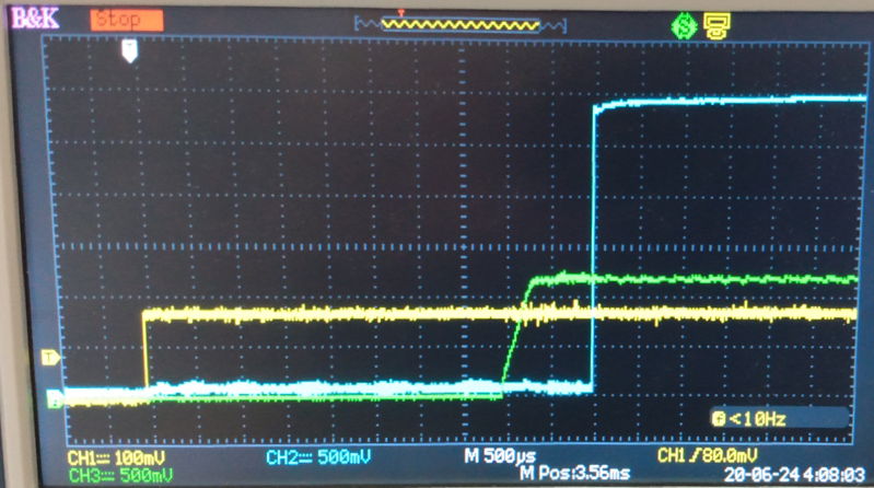
Figure: Power-Up Sequence. Yellow: VR in response to turning on 910 MHz. Green: 1V2 generated by buck converter U1. Blue: Copy of RP generated by U8 test point output, shows when U8 is configured and running.
The buck converter takes 4.5 ms to turn on 1V2. This adds to the start-up time of U8, which is visible above as the 0.7-ms delay between the green and blue traces. The A3037A is unable to receive commands with an initiate pulse of 5 ms. We increase initiate_delay from 0.005 to 0.010 in the Stimulator Tool configuration panel. Command reception is reliable, as shown below.
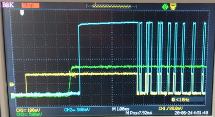
Figure: Command Reception. Yellow: VR in response to turning on 910 MHz. Green: 1V2 generated by buck converter U1. Blue: Copy of RP generated by U8 test point output.
We turn on stimulation and look at ONL, which is bursts of 32 kHz when we want the lamp to turn on. We connect a lamp and resistor to L+/L−. We have 3.7 V connected to VBS and VBR. The rectified signal R is equal to the feedthrough signal F. With a multimeter we get inconsistent values for forward and reverse resistance of D5, but never a short circuit.
[24-JUN-20] We check the package markings on D1 and D5 and find they are correct: D1 is the SMS7630-040LF with marking "P" and D5 is the SMS7621-040LF with the marking "F". We replace D5 on No1 with SMS7621-040LF and we get the following switching performance from the isolator.
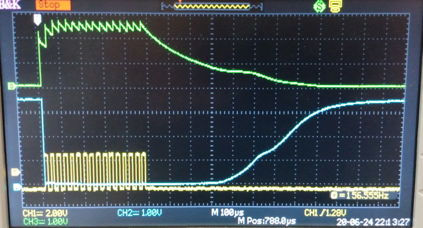
Figure: Isolator Operation on the A3037A. Yellow: ONL. Blue: L−. Green: R, as in S3037A_2. We have commanded the A3037A to generate 0.5-ms light pulses with a white LED in series with a 50-Ω resistor.
Turn-on time is less than 100 ns. Turn-off time is 400 μs. The 500-μs pulses we request turn out to be 900-μs pulses. On board No3, we have the same problem as with No1 before replacing D5. We replace D5 and the isolator functions perfectly. We start work on No2, trying to measure forward and reverse resistance of the existing D5. We get 150 Ω in forward direction with 200-Ω range, and >200 Ω in reverse direction. But with 2-kΩ range we see 80 Ω and −80 Ω respectively. The isolator has the same problem as No1 and No3. We replace D5 and now it works perfectly. We put our multimeter on 20-kΩ range and measure 15-16 kΩ forward resistance on all three boards. On 20 MΩ range we measure 1.1-1.7 MΩ reverse resistance on all three boards. We finalize firmware P3037A01.
We add ADC readout to P3037A02. When we have CONV tied low we note that current consumption is 450 μA. When we have the digitization working, current consumption at 1024 SPS is 23 μA higher than with no digitization. We check gain versus frequency and find the shape of the response is correct, but gain is for all frequencies a factor of twenty too low. We find that R6, R15, R16, and R17 are all 1 MΩ when they are supposed to be 50 kΩ. But R2, R3, R8, R9, and R10 are all 1 MΩ also, as they should be. The BOM used by the assembly house has all nine of these resistors set to 1 MΩ. We replace R6 with 50 kΩ and now gain versus frequency is perfect.
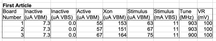
Figure: Properties of First Three A3037AV1 Circuits. Currents drawn either from VBM or VBS. Active is negligible pulses and continuous stimulus. Xon is sensor data transmission at 1024 SPS. Stimulus is a white LED with 50-Ω resistor shining continuously. Tuning is response to 10-dBm sweep in favorable antenna location, peak frequency and height at VR.
From these measurements, we deduce the following current consumption characteristics for the circuit.
| Property | Value |
|---|
| Inactive Current, Master Battery | 7.3 μA |
| Active Quiescent Current, Master Battery | 60 μA |
| Stimulus Off Current, Stimulus Battery | 0.0 μA |
| Stimulus On Current, Master Battery | 8 μA |
| Data Transmission Current, Master Battery | 0.078 μA/SPS |
| Digitization and Storage Current, Master Battery | 0.022 μA/SPS |
| Total Transmission Current, Master Battery | 0.10 μA/SPS |
| Inactive Life | 57 day |
| Data Transmit Life at 128 SPS | 140 hr |
Table: Properties of the A3037AV1. Assume 10-mAhr master and stimulator battery capacity.
Modifications to the A303701A circuit board: adjust silk screen around P5, because L− and VBS labels are swapped.
[10-JUL-20] On 03-JUL-20 we started A3037A 0002 generating a 10-ms flash of a white LED with 50-Ω series resistor every 5000 ms. We turned off synchronizing signal. Seven days later, the stimulus is still running. We measure VBM = 3.73 V and VBS = 3.75 V. We measure current versus forward voltage in the diode of Q1, so as to inform our design of a charger for the stimulus battery.
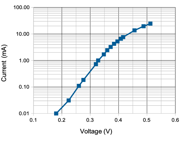
Figure: Current versus Voltage for Charging Diode in the Stimulator Circuit. This diodes it the clamping diode of the stimulator switch, an RYM002N05 mosfet.
[13-JUL-20] After 240 hrs, our stimulus is still running on 0002, VBM = 3.2 V, VBS = 3.7 V. According to our calibration of 0002, active current is 57 μA, so 240 hrs suggests capacity 13.7 mA. We start re-charging the master battery. We have 11 mA flowing in at 3.7 V.
[28-JUL-20] On 15-JUL-20 both 0002 batteries are fully charged. At 13:40 we start it running with a 10-ms flash every five seconds. On 21-JUL-20 it is flashing at 16:00. On 23-JUL-20 it is not flashing at 10:00. This time our battery life was no more than 180 hrs. VBM = 2.6 V, VBS = 3.9 V. We re-charge both batteries.
[29-JUL-20] We have recharged VBM to 4.2 V, waiting until charge current has settled to 70 μA. We initiate 10-ms flashes every 5000 ms.
[06-AUG-20] Our 0002 board is still flashing, VBM = 3.76 V, VBS = 3.80 V. We have 17 more A3037AV1 assemblies. We tune all crystal radios. Most are correct as assembled with C6 = 1.0 pF and C19 = 0.2 pF, but in some we increase the sum of these two by 0.1 pF.
[07-AUG-20] Our 0002 board still flashing, VBM = 3.60 V at 11:00. At 14:00 VBM = 3.52 V. Battery life 220 hrs. We recharge partially with an A3033C, then make the board available for encapsulation.
[24-AUG-20] We have twenty A3037A circuits programmed and calibrated, but several days after programming, their ring oscillators are unstable. We encapsulate one such circuit, which we photograph for the manual. Volume is 1.7 ml, mass 2.7 g. The FCK period of all devices is fluctuating by about ±5 ns. All eighteen devices present this fluctuation. We re-program with various values of fck_divisor, but the effect persists. We check routing of ring oscillator and find all gates to be clustered together. We modify the way in which the ring oscillator clocks the divider, but the effect persists. We change the sample rate between 512 SPS and 1024 SPS, no effect. We observe that the core logic supply for U8 (1V2) fluctuates by ± 20 mV, consistent with our operation of the ADP5301 in hysteresis mode. We measure FCK period and 1V2 for repeated transmit bursts.
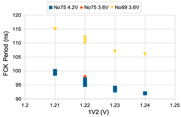
Figure: FCK Period versus Core Logic Supply Voltage (1V2). We vary the battery power supply voltage and device as well, see legend.
We conclude that the gate propagation delay in U8 varies with core power supply voltage by roughly −3%/10mV. Because of these fluctuations, reception from a typical A3037A is only 90%. During this work, we find that reception of commands with boost power over a range of one meter is reliable. In a future design, we could set the output of the ADP5301 to 1.5 V and regulate down to 1.2 V with a micropower regulator. For this design, however, we suggest setting the maximum FCK period in the range 105-110 ns, so that the minimum period will be >97 ns and the maximum ≤110 ns. Our ring oscillator code provides steps of 5 ns in FCK period, but its resolution could be further improved if necessary. Right now, with a typical value for fck_divisor of 16, the ring contains 8 gates, so that its oscillation period is 16 propagation delays, or 16τ, while the divisor is 8. So the nominal 100-ns FCK period is 128τ, making τ ≈ 800 ps.
[26-AUG-20] When we program the A3037A, the maximum current drawn from VBM is 10 mA and the minimum is 3 mA. Compare this to 25 mA maximum and 3 mA minimum from VB for the A3036B. We conclude that the programmer itself draws 3 mA from 3V0, but the XO2-1200ZE draws 22 mA from 1V2, which appears as 7 mA from VBM in the A3037A because of the 90% efficient conversion from 3.7 V to 1.2 V.
We have A3037A No69 and we observe its FCK period varying from 106-115 ns. We freeze it to −40°C and observe range 107-115 ns. We re-configure the ring oscillator, producing P3037A02_OSC.vid, in which we create a ring oscillator of constant length five gates, which we divide by 10-25 according to fck_divisor. We compile and program No69 with divisor 18 down to 14 twice. Reception for divisor 15 and 16 is 99.5%. Our resolution in FCK period is uncertain.
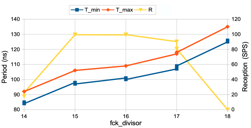
Figure: FCK Min and Max Period and Reception versus Divisor. We have the maximum and minimum FCK period, and the maximum reception as a percentage, for fck_divisor in likely range.
[28-AUG-20] We equip one A3037A with two batteries loaded directly on the circuit board, and a lamp. We equip another with only the VBM battery on a 100-mm cable connected to the programming extension. We leave their X inputs open-circuit. Both circuits are un-encapsulated, and have their programming and test extensions. We initiate 100 ms pulses with 500 ms period and see the same lamp artifact in both devices.
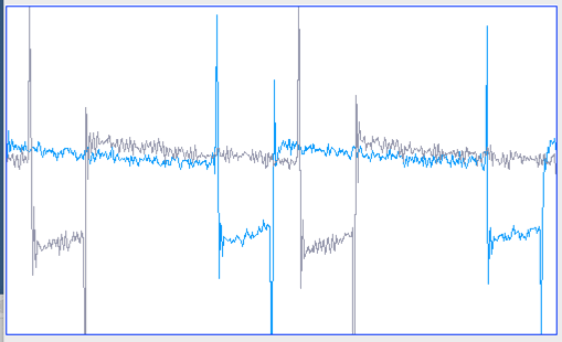
Figure: Lamp Control Artifact, Open Circuit. Full range 2000 counts = 920 μV. Blue: With both batteries and lamp flashing. Gray: With only master battery and no lamp.
The open-circuit lamp artifact is around 900 μVpp. We connect X and C with jumper and the artifact disappears. We change to 10 ms pulses at 10 Hz and obtain the spectrum of a 32-s interval.
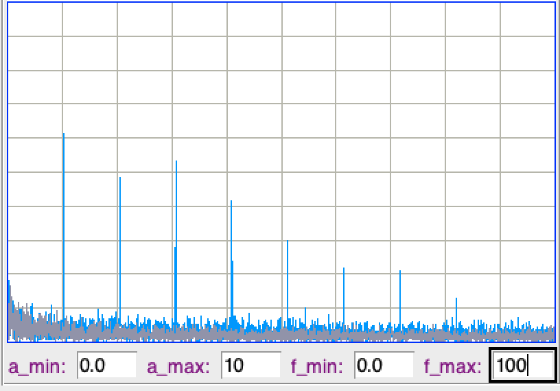
Figure: Lamp Control Artifact Spectrum, Short Circuit. Full range 10 counts = 460 nV. Blue: With both batteries and lamp flashing. Gray: With only master battery and no lamp.
The on-board lamp artifact with inputs shorted is around 10 μVpp, total noise 1-160 Hz 7.8 μV. We replace the short with 1 MΩ and see 400 Vpp artifact. At 100 kΩ we see 90 μVpp. At 10 kΩ, we see 5 μVpp. We load two batteries to each of No68, 69, 78, and 83, and secure each battery to the circuit board with a drop of super-glue so as to stop them rising up, which would otherwise increase the final volume.
[31-AUG-20] We add to P3037A03.vhd firmware a new command set_start_condition. We turn on data transmission and set the start condition to one. When the ADC sample jumps by more than 16k counts, we initiate a stimulus. We obtain this video of initiating stimulus by touching the X input.
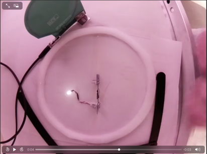
Figure: Closed-Loop Response Demonstration. The A3037A initiates stimulus when we touch the sensor input.
Fall-20
[09-OCT-20] We have 4 of A3037A encapsulated, No68, 69, 78, and 83. Their combined displacement volume is 7 ml, making each of them 1.8 ml. Batteries are flush to the circuit boards. Silicone is thick enough to smooth over battery corners. Three work perfectly, No83 will not respond to commands. We connect No83 to an A3033C charger. We place No68, 69, and 78 in water, turn on signal transmission, and flash the lamp with 10-ms pulses at 10 Hz. The following table shows the lamp artifact induced in each of the three X inputs by each of the three stimulators, with the signal inputs separated by 1 mm of air or 1 mm of water.
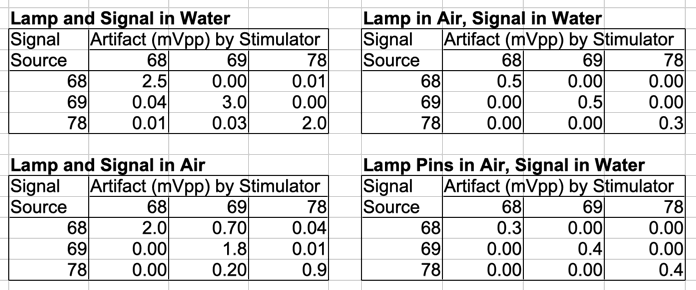
Figure: Lamp Artifact for Various Arrangements.
When we transmit one command immediately after another with the Stimulator Tool's Start_All button, command reception is 90% reliable. When we press the individual stimulator Start buttons one after the other, command reception is 100% reliable with acknowledgment received. We add a delay of 100 ms between the commands of the _All commands using a new spacing_delay_cmd, but still lose 10% of commands. After an hour on the charger, No83 works well.
We place No69 and signal leads in water, lamp out of water. We flash lamp at 10 Hz, 10 ms pulses. Artifact is 400 μVpp. Add salt to water and stirr. Artifact is 30 μVpp. Separate leads in saltwater by 50 mm, artifact remains 20 μVpp. Place lamp in water, 50 mm from signal leads, which are close together. Artifact is 1 mVpp. We place stimulator in one saltwater dish along with sensor electrodes, and the lamp in another saltwater dish. Artifact 50 μVpp. Connect two dishes with 100-kΩ resistor, artifact 800 μVpp. With 1 MΩ, 700 μVpp. With 10 MΩ 600 μVpp.
Response of the four A3037As to 20-MΩ sweep is correct. We place in water and find total noise in 1-160 Hz is 6-7 μV rms for all four. But we see steady, sharp peaks in the spectrum, as shown below.
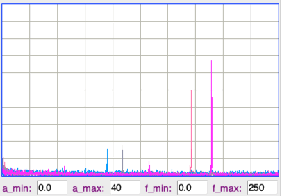
Figure: Noise Spectrum of Four A3037A in Water. Vertical scale 200 μV/div, horizontal 25 Hz/div.
[12-OCT-20] We turn on data transmission from A215.78 and measure impedance between X−, which is VC = 1.2 V, and L+, which is VBS. We get >200 MΩ in parallel with 131 pF. We expect the capacitance to be C16 = 100 pF in parallel with the capacitance between ONL and Q1-3. The capacitance ONL to Q1-3 is C15 = 100 pF in series with the 40-pF RYM002N05 gate capacitance. So we expect 100 pF in parallel with 29 pF is 129 pF and we see 131 pF. We make the same measurement for No69, No83, and No68 and get 132 pF, 133 pF, and 132 pF, with >200 MΩ in all.
[15-OCT-20] We set A215.69 flashing at 10 Hz with 50-ms pulses. We remove the lamp. We connect our oscilloscope probe to L+, the orange lead, and the ground to C, the blue lead. We are measuring the voltage between VC, which is connected to 1.2V through 1 kΩ and VBS, the stimulator battery positive terminal. We see the following.
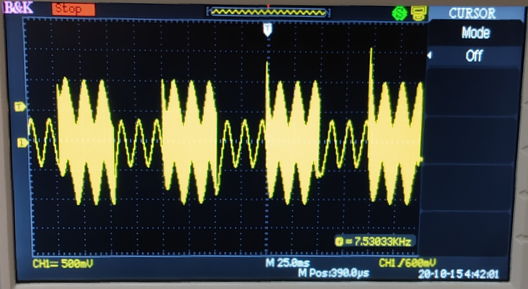
Figure: VBS versus VC during 50-ms Pulses at 10 Hz, no lamp attached.
The low frequency is 60 Hz mains hum, which we find hard to eliminate with the probe ground attached to one of the circuits. The high-frequency pulses, when we examine them in detail, are a 32.768 kHz square wave.
[16-OCT-20] We place A215.78 on a petri dish with X+ and X− connected by a copper clip. We flash an A3036IL-A with the stimulus pins, 10-ms pulses at 10 Hz. We examine the spectrum of the X signal. Lamp artifact is <1 μVpp. Remove clip, lamp artifact is 1.2 mVpp. Connect X leads again, place in water with device body, lamp out of water, artifact 20 μVpp. Place lamp in water near shorted leads, 5 mVpp artifact. Move lamp out of water again, artifact <8 μVpp. Disconnect leads, immerse leads and body in 1% saline, separate leads by 50 mm, lamp out of water, artifact <1 μVpp, total noise 6 μV rms. Repeat in pure water, artifact 400 μVpp. Back to saline, < 1 μVpp. Place lamp in saline, artifact 1 mVpp. Same thing in pure water, 5 mVpp. Wrap lamp in kapton tape, pull stimulator leads to get water to wick into tape, place in saline with body and sensor leads, artifact 200 μVpp. Move taped lamp out of water, <1 μVpp.
[20-OCT-20] We hoist U7-3, disconnecting it from VC, on A215.85, an A3037AV1 assembly with extensions. We apply 4.0 V to VBM. We measure resistance from U7-3 to 0VM and get 4.3 MΩ with red lead on U7-3, and 4.1 MΩ with red lead on 0VM. We try another meter and get 5.7 MΩ with red lead on U7-3.
[01-DEC-20] We are assembling a new patch of A3037A and we find that several of ten no longer transmit after clipping the programming extension. One of them works fine after we grind the clipped edge. We grind all the clipped edges. No others recover.
Winter-21
[18-JAN-21] We replace our capacitive isolator with an optoisolator. We use the CTP17 we tested earlier. We remove C15 and C16. We wire ONL through 100 kΩ to anode of optoisolator's, and 0V to cathode. In place of D5 we load 0 Ω, in place of R14 we load 100 kΩ. We wire collector of optoisolator to VBS and emitter to Q1-3, F.

Figure: CTP17 Optoisolator Modification.
We re-program the A3037A to create the first A3037B, in which ONL is equal to PA, Pulse Active, without modulation at 32.768 kHz. We connect two LiPo batteries. We use ONL as our trigger and look at the optoisolator anode and emitter. We initiate pulses of 5 ms with period 20 ms. We connect a white LED with 51-Ω series resistor to L+ and L−. The light shines brightly.
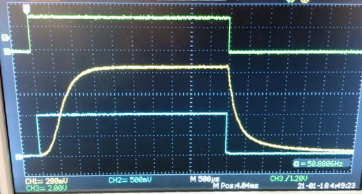
Figure: CTP17 Switching Signals. We have ONL (Green, 2 V/div), optoisolator anode (blue, 500 mV/div), and optoisolator emitter, which is also the gate of Q1 (yellow, 200 mV/div). Timebase 500 μs/div.
When the lamp is on we have 1 V across the optoisolator's LED and 2 V across the 100-kΩ drive resistor for 20 μA forward current. Turning the lamp on costs 20 μA from the master battery. A 10-Hz stimulus of 10-ms pulses will consume 2 μA, which is insignificant compared to the active current consumption of at least 100 μA. We see the voltage on the gate of Q1, which is the voltage across R14 = 100 kΩ, rise over 1 ms to 800 mV, which is sufficient to turn on the RYM002N05. Fall time for turn-off is another 1 ms. The voltage across the 51-Ω resistor in series with the white LED is 800 mV, implying 16 mA LED current. We set the lamp to flashing at 10 Hz, 20-ms pulses. We turn on data transmission and observe lamp artifact with the X input open-circuit (10-MΩ input impedance).
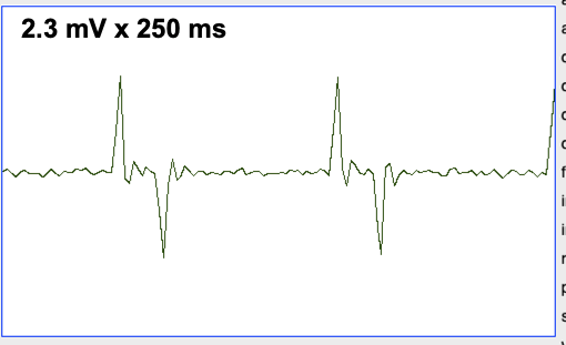
Figure: Opto-Isolator Lamp Artifact for 10 MΩ Amplifier Input Impedance.
This artifact is a high-pass filtered version of the lamp control signal, with time constant of order 2 ms, which we can see with our 160-Hz filter and 1024 SPS sample rate. We will call it edge noise. We stop the lamp flashing, input noise is 50 μVpp. We resume lamp flashing, but remove the lamp itself, edge noise is 1 mVpp. We remove the stimulator battery as well and see no trace of edge noise in the trace, but we do see a 2-μV peak at 10 Hz in the spectrum. We restore the stimulator battery and the lamp. We connect 1 MΩ to the X input and see the edge noise drop from 1 mVpp to 100 μVpp.
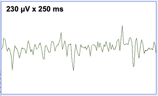
Figure: Opto-Isolator Lamp Artifact for 1 MΩ Amplifier Input Impedance.
With 100 kΩ input impedance, we cannot see edge noise in the signal as displayed above. But if we record with the Neuroarchiver and take the Fourier transform of a 32-s interval, we see a peak at 10 Hz that is 1.6 μV. We measure the amplitude of this 10-Hz fundamental with amplifier input impedance.
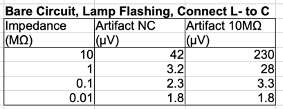
Figure: Amplitude of 10-Hz Fundamental Harmonic Lamp Artifact versus Input Impedance. We have 10-Hz flashing of 20-ms pulses. First we have no connection (NC) between L− and C, then 10 MΩ between the two. In all cases, if we can see the artifact in the signal trace, it is edge noise with zero average value.
With our capacitive isolator, the artifact was dominated by negative steps that arose even without the stimulator battery connected. These negative steps have vanished. We are left with edge noise that persist when the lamp is disconnected and when we remove R15, but not when we disconnect the stimulator battery. We flash the lamp and short X to L−. With 10 MΩ input impedance and see full-scale (30 mV) artifact of the same form. With 10 kΩ input impedance, we see 400 μVpp. We connect L− to C with 10 MΩ and flash the lamp at 10 Hz with 20 ms pulses. We vary the amplifier input impedance from 10 MΩ down to 10 kΩ and measure the amplitude of the 10-Hz fundamental of the edge noise. We add our measurements to the table above. We prepare the second page of the schematic for the A3037B, S3037B_2.
[26-JAN-21] We have an encapsulated A3037B (B215.84), made with two 25-mAhr LiPo batteries. We immerse the body and sensor leads in one cup of saline and the lamp and lamp leads in another cup of saline. We place an A3028S2-AA (S217.55) in the same cup as the A3037B. We set the lamp to flashing for 200 ms at 1 Hz. We connect the two cups with various resistors, including open-circuit and short-circuit. We record the lamp artifact in one-second intervals.
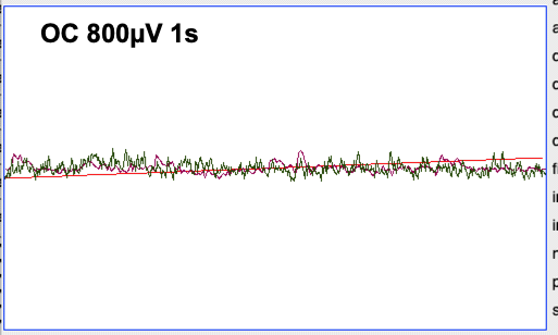
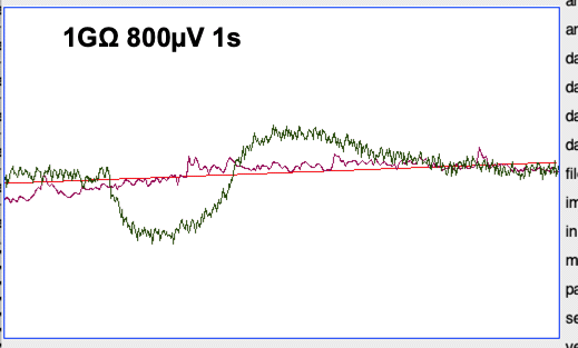
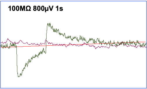
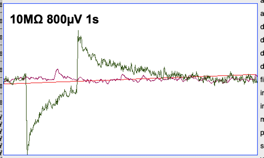
Figure: Lamp Artifact for Saline Reservoirs Connected by Various Resistors. Black: A3037B-AA, Brown: A3028S2-AA. Red: Clock Signal (inclusion accidental). The A3038B input impedance is 100 kΩ
These are step artifacts with a decay constant of around 300 ms, which is consistent with our 0.3-Hz high-pass filter. The 50-ms time constant of the first edge with 1 GΩ is consistent with a 50-pF capacitor being charged.
[27-JAN-21] Repeat above experiments, find that size of artifact depends upon resistance between X and C electrodes. Hold them 1 mm apart in reservoir with A3037B and 10 MΩ connection to lamp reservoir, get 400 μV steps. Hold them 1 mm apart out of water see no step, but noise burst when lamp turns on and off. Short together outside water, no artifact whatsoever. Short together in reservoir, no artifact whatsoever. Separate by 0.5 mm in water, 200-μV step artifact. Connect the two leads with 10 kΩ P0805 resistor, no artifact whatsoever. Note that B215.84 has R5 = 10 MΩ. Place lamp and sensor leads in same reservoir, 20 mm from sensor leads, sensor leads joined by 10 kΩ, no artifact whatsoever. Move lamp to within 5 mm of sensor leads, see 400-μV, 1-ms pulses in opposite directions when lamp turns on and off. Try 100 kΩ with lamp and sensor in same reservoir of saline, separated by 40 mm. We see 1-ms, 80-μV pulses on a background noise of 80 μVpp. We put lamp in separate reservoir with 10-MΩ connection, leaving 100-kΩ resistor between sensor leads. Flash 10-ms pulses at 10 Hz and record for 60 s, see M1611791347.ndf.
Figure: Spectrum Lamp Artifact for 10-ms Pulses at 10 Hz. We have 10 MΩ between lamp and sensor reservoirs, 100 kΩ soldered between X and C.
The amplitude of the artifact is 25 μV. When we turn off the lamp, noise is 13 μV. We add R26, 100 kΩ, across X and C in the S3037B_1, and preserve the 50-V 100-nF with 10 MΩ beyond R26 to give us the 0.3-Hz high-pass filter.
[28-JAN-21] We place A3037B lamp and sensor leads in the same 1% saline reservoir. We flash the lamp at 10 Hz with 10-ms pulses. The lamp leads are 5 mm from the sensor leads. The sensor leads are terminated by 100 kΩ.
Figure: Lamp Artifact, Worst Case with 100 kΩ Input Resistance. Lamp and sensor leads 5 mm from one another in 1% saline. No insulation around lamp pins.
We separate the lamp and sensor leads into two reservoirs, with body of A3037B in reservoir with sensor leads. We have 100 kΩ soldered to the ends of the sensor leads. We join the reservoirs with various resistors.
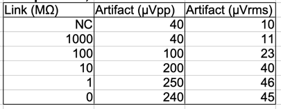
Figure: Lamp Artifact With Two Reservoirs for Various Reservoir Link Resistances. We have 100 kΩ soldered to the tips of the sensor leads, and a green LED connected to the stimulator leads.
We have 10 MΩ link resistor and 200 μVpp artifact. Removing the A3037B body from the reservoir has little effect on artifact. Placing the body in the lamp reservoir has little effect. Lamp leads in water, sensor lead out of water, artifact drops to 40 μVpp. Lamp leads out of water, sensor leads in water, artifact disappears. Restore lamp and sensor leads to their reservoirs, separate sensor leads except at base and tip, artifact drops to 90 μVpp. Run sensor leads together again, artifact rises only to 110 μVpp. Sensor leads in air, tips in water, artifact rises to 270 μVpp. Re-immerse sensor leads together in water, artifact remains 270 μVpp. Run lamp leads out of water all the way to lamp, artifact 130 μVpp. Disconnect lamp, artifact 120 μVpp average value zero.
Take un-encapsulated A3037B number B215_85. Connect two batteries and 100 kΩ across X and C, immerse sensor leads in one reservoir and lamp leads in another, connect with 10 MΩ, artifact 180 μVpp, but pulses have average value zero.
Return to encapsulated B215_84. With an SCT in the same reservoir as the sensor leads, and the lamp leads in separate reservoir with link 10 MΩ, we try to get lamp artifact in the SCT signal, but see none. When we place the SCT in the same reservoir as the lamp, we get up to 10 mVpp artifact.
[29-JAN-21] Measure resistance between L+ and C and get >100 GΩ, capacitance using function generator and series resistor 50±20 pF. Set up the same two-reservoir experiment with 1% saline and 10 MΩ, all leads immersed, 100 kΩ on sensor leads, 10-ms pulses at 10 Hz and today we see symmetric artifact of 200 μVpp. Move sensor leads out of water, with only tips in the water, see 200 μVpp. Add salt to make 2% saline, see 200 μV. In hot 2% saline, transmission continues but lamp stops flashing, even with sensor body out of water. We immerse the lamp only in water and it stops flashing. The artifact remains about 200 μVpp. Lamp current is flowing through the saltwater between the lamp sockets instead of through the lamp.
Solder our lamp leads to our lamp. Put a few drops of dental cement on the solder joints. Allow to cure. Place in a beaker of warm 1% saline along with A3037B body and sensor leads terminated with 100 kΩ. No visible lamp artifact. Record 600 s of sensor signal in M1611953882.ndf. In first minute, artifact is a 30-μV pulse down when lamp turns on, 30 μV pulse up when lamp turns off. The pulses grow to 40 μV by the end of 100-s stimulus. By the end of recording, artifact is 80 μV pulses. We see another oscillation in the recording, which starts at 7 Hz and ends at 30 Hz, even as heating fans turn on and off. We see no such noise in earlier recording of artifact M1611791347.ndf.
[09-FEB-21] We use the following processor to remove the fundamental and harmonics of lamp artifact from the signal recorded in M1611953882.ndf.
set f_artifact [expr 82.0 / 8.0]
set filtered_spectrum ""
set f 0.0
foreach {a p} $info(spectrum) {
	if {(fmod($f+0.5,$f_artifact) <= 1.0) && ($f > $f_artifact - 1.0)} {
		append filtered_spectrum "0.0 0.0 "
		Neuroarchiver_print "$f $a $p"
	} {
		append filtered_spectrum "$a $p "
	}
	set f [expr $f + $info(f_step)]
}
set filtered_values [lwdaq_fft $filtered_spectrum -inverse 1]
set filtered_signal ""
set timestamp 0
foreach v $filtered_values {
	append filtered_signal "$timestamp $v "
	incr timestamp
}
Neuroarchiver_plot_signal 5 $filtered_signal
append result "$info(channel_num) [format %.2f $f_artifact] "
We remove all components within 0.5 Hz of the fundamental and harmonics, and we find that the actual frequency of the flashes is 10.25 Hz when we ask for 10.00 Hz. The result of the subtraction is shown below. We see the lamp artifact removed, but the other unexplained, non-lamp artifact in the recording remains intact.
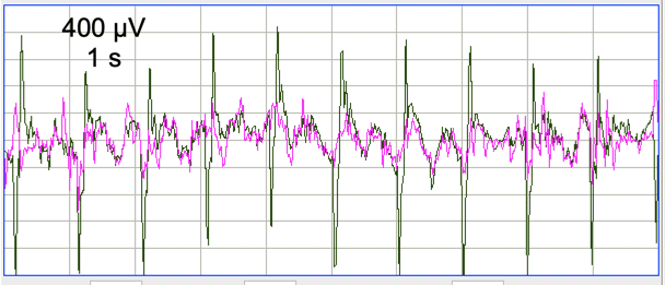
Figure: Lamp Artifact Removed by Filtering.
[12-NOV-21] We review observations of lamp artifact in A3037B. Internal lamp artifact is generated by the 3.6-V lamp signal coupling through the 50-pF capacitance between the master and stimulator and into the amplifier input. With input impedance ≤1 MΩ, the artifact is invisible to our 160-Hz bandwidth. Having reduced the input impedance to 100 kΩ, we have eliminated the internal artifact. The remaining artifact arises from the electric field generated by the lamp pins, and also from the additional master-stimulator capacitance provided by the sensor and lamp leads in water.